EP1321976A2 - Procédé de dépôt d'une couche barrière isolante à faible constante diélectrique sur une couche de cuivre - Google Patents
Procédé de dépôt d'une couche barrière isolante à faible constante diélectrique sur une couche de cuivre Download PDFInfo
- Publication number
- EP1321976A2 EP1321976A2 EP02024920A EP02024920A EP1321976A2 EP 1321976 A2 EP1321976 A2 EP 1321976A2 EP 02024920 A EP02024920 A EP 02024920A EP 02024920 A EP02024920 A EP 02024920A EP 1321976 A2 EP1321976 A2 EP 1321976A2
- Authority
- EP
- European Patent Office
- Prior art keywords
- gas
- insulating film
- film forming
- film
- dielectric constant
- Prior art date
- Legal status (The legal status is an assumption and is not a legal conclusion. Google has not performed a legal analysis and makes no representation as to the accuracy of the status listed.)
- Withdrawn
Links
Images








Classifications
-
- H—ELECTRICITY
- H10—SEMICONDUCTOR DEVICES; ELECTRIC SOLID-STATE DEVICES NOT OTHERWISE PROVIDED FOR
- H10P—GENERIC PROCESSES OR APPARATUS FOR THE MANUFACTURE OR TREATMENT OF DEVICES COVERED BY CLASS H10
- H10P14/00—Formation of materials, e.g. in the shape of layers or pillars
- H10P14/60—Formation of materials, e.g. in the shape of layers or pillars of insulating materials
- H10P14/69—Inorganic materials
- H10P14/692—Inorganic materials composed of oxides, glassy oxides or oxide-based glasses
- H10P14/6921—Inorganic materials composed of oxides, glassy oxides or oxide-based glasses containing silicon
- H10P14/6922—Inorganic materials composed of oxides, glassy oxides or oxide-based glasses containing silicon the material containing Si, O and at least one of H, N, C, F or other non-metal elements, e.g. SiOC, SiOC:H or SiONC
-
- C—CHEMISTRY; METALLURGY
- C23—COATING METALLIC MATERIAL; COATING MATERIAL WITH METALLIC MATERIAL; CHEMICAL SURFACE TREATMENT; DIFFUSION TREATMENT OF METALLIC MATERIAL; COATING BY VACUUM EVAPORATION, BY SPUTTERING, BY ION IMPLANTATION OR BY CHEMICAL VAPOUR DEPOSITION, IN GENERAL; INHIBITING CORROSION OF METALLIC MATERIAL OR INCRUSTATION IN GENERAL
- C23C—COATING METALLIC MATERIAL; COATING MATERIAL WITH METALLIC MATERIAL; SURFACE TREATMENT OF METALLIC MATERIAL BY DIFFUSION INTO THE SURFACE, BY CHEMICAL CONVERSION OR SUBSTITUTION; COATING BY VACUUM EVAPORATION, BY SPUTTERING, BY ION IMPLANTATION OR BY CHEMICAL VAPOUR DEPOSITION, IN GENERAL
- C23C16/00—Chemical coating by decomposition of gaseous compounds, without leaving reaction products of surface material in the coating, i.e. chemical vapour deposition [CVD] processes
- C23C16/22—Chemical coating by decomposition of gaseous compounds, without leaving reaction products of surface material in the coating, i.e. chemical vapour deposition [CVD] processes characterised by the deposition of inorganic material, other than metallic material
- C23C16/30—Deposition of compounds, mixtures or solid solutions, e.g. borides, carbides, nitrides
- C23C16/308—Oxynitrides
-
- C—CHEMISTRY; METALLURGY
- C23—COATING METALLIC MATERIAL; COATING MATERIAL WITH METALLIC MATERIAL; CHEMICAL SURFACE TREATMENT; DIFFUSION TREATMENT OF METALLIC MATERIAL; COATING BY VACUUM EVAPORATION, BY SPUTTERING, BY ION IMPLANTATION OR BY CHEMICAL VAPOUR DEPOSITION, IN GENERAL; INHIBITING CORROSION OF METALLIC MATERIAL OR INCRUSTATION IN GENERAL
- C23C—COATING METALLIC MATERIAL; COATING MATERIAL WITH METALLIC MATERIAL; SURFACE TREATMENT OF METALLIC MATERIAL BY DIFFUSION INTO THE SURFACE, BY CHEMICAL CONVERSION OR SUBSTITUTION; COATING BY VACUUM EVAPORATION, BY SPUTTERING, BY ION IMPLANTATION OR BY CHEMICAL VAPOUR DEPOSITION, IN GENERAL
- C23C16/00—Chemical coating by decomposition of gaseous compounds, without leaving reaction products of surface material in the coating, i.e. chemical vapour deposition [CVD] processes
- C23C16/22—Chemical coating by decomposition of gaseous compounds, without leaving reaction products of surface material in the coating, i.e. chemical vapour deposition [CVD] processes characterised by the deposition of inorganic material, other than metallic material
- C23C16/30—Deposition of compounds, mixtures or solid solutions, e.g. borides, carbides, nitrides
- C23C16/40—Oxides
- C23C16/401—Oxides containing silicon
-
- C—CHEMISTRY; METALLURGY
- C23—COATING METALLIC MATERIAL; COATING MATERIAL WITH METALLIC MATERIAL; CHEMICAL SURFACE TREATMENT; DIFFUSION TREATMENT OF METALLIC MATERIAL; COATING BY VACUUM EVAPORATION, BY SPUTTERING, BY ION IMPLANTATION OR BY CHEMICAL VAPOUR DEPOSITION, IN GENERAL; INHIBITING CORROSION OF METALLIC MATERIAL OR INCRUSTATION IN GENERAL
- C23C—COATING METALLIC MATERIAL; COATING MATERIAL WITH METALLIC MATERIAL; SURFACE TREATMENT OF METALLIC MATERIAL BY DIFFUSION INTO THE SURFACE, BY CHEMICAL CONVERSION OR SUBSTITUTION; COATING BY VACUUM EVAPORATION, BY SPUTTERING, BY ION IMPLANTATION OR BY CHEMICAL VAPOUR DEPOSITION, IN GENERAL
- C23C16/00—Chemical coating by decomposition of gaseous compounds, without leaving reaction products of surface material in the coating, i.e. chemical vapour deposition [CVD] processes
- C23C16/44—Chemical coating by decomposition of gaseous compounds, without leaving reaction products of surface material in the coating, i.e. chemical vapour deposition [CVD] processes characterised by the method of coating
- C23C16/455—Chemical coating by decomposition of gaseous compounds, without leaving reaction products of surface material in the coating, i.e. chemical vapour deposition [CVD] processes characterised by the method of coating characterised by the method used for introducing gases into reaction chamber or for modifying gas flows in reaction chamber
-
- C—CHEMISTRY; METALLURGY
- C23—COATING METALLIC MATERIAL; COATING MATERIAL WITH METALLIC MATERIAL; CHEMICAL SURFACE TREATMENT; DIFFUSION TREATMENT OF METALLIC MATERIAL; COATING BY VACUUM EVAPORATION, BY SPUTTERING, BY ION IMPLANTATION OR BY CHEMICAL VAPOUR DEPOSITION, IN GENERAL; INHIBITING CORROSION OF METALLIC MATERIAL OR INCRUSTATION IN GENERAL
- C23C—COATING METALLIC MATERIAL; COATING MATERIAL WITH METALLIC MATERIAL; SURFACE TREATMENT OF METALLIC MATERIAL BY DIFFUSION INTO THE SURFACE, BY CHEMICAL CONVERSION OR SUBSTITUTION; COATING BY VACUUM EVAPORATION, BY SPUTTERING, BY ION IMPLANTATION OR BY CHEMICAL VAPOUR DEPOSITION, IN GENERAL
- C23C16/00—Chemical coating by decomposition of gaseous compounds, without leaving reaction products of surface material in the coating, i.e. chemical vapour deposition [CVD] processes
- C23C16/44—Chemical coating by decomposition of gaseous compounds, without leaving reaction products of surface material in the coating, i.e. chemical vapour deposition [CVD] processes characterised by the method of coating
- C23C16/455—Chemical coating by decomposition of gaseous compounds, without leaving reaction products of surface material in the coating, i.e. chemical vapour deposition [CVD] processes characterised by the method of coating characterised by the method used for introducing gases into reaction chamber or for modifying gas flows in reaction chamber
- C23C16/45557—Pulsed pressure or control pressure
-
- C—CHEMISTRY; METALLURGY
- C23—COATING METALLIC MATERIAL; COATING MATERIAL WITH METALLIC MATERIAL; CHEMICAL SURFACE TREATMENT; DIFFUSION TREATMENT OF METALLIC MATERIAL; COATING BY VACUUM EVAPORATION, BY SPUTTERING, BY ION IMPLANTATION OR BY CHEMICAL VAPOUR DEPOSITION, IN GENERAL; INHIBITING CORROSION OF METALLIC MATERIAL OR INCRUSTATION IN GENERAL
- C23C—COATING METALLIC MATERIAL; COATING MATERIAL WITH METALLIC MATERIAL; SURFACE TREATMENT OF METALLIC MATERIAL BY DIFFUSION INTO THE SURFACE, BY CHEMICAL CONVERSION OR SUBSTITUTION; COATING BY VACUUM EVAPORATION, BY SPUTTERING, BY ION IMPLANTATION OR BY CHEMICAL VAPOUR DEPOSITION, IN GENERAL
- C23C16/00—Chemical coating by decomposition of gaseous compounds, without leaving reaction products of surface material in the coating, i.e. chemical vapour deposition [CVD] processes
- C23C16/44—Chemical coating by decomposition of gaseous compounds, without leaving reaction products of surface material in the coating, i.e. chemical vapour deposition [CVD] processes characterised by the method of coating
- C23C16/50—Chemical coating by decomposition of gaseous compounds, without leaving reaction products of surface material in the coating, i.e. chemical vapour deposition [CVD] processes characterised by the method of coating using electric discharges
- C23C16/505—Chemical coating by decomposition of gaseous compounds, without leaving reaction products of surface material in the coating, i.e. chemical vapour deposition [CVD] processes characterised by the method of coating using electric discharges using radio frequency discharges
-
- H—ELECTRICITY
- H10—SEMICONDUCTOR DEVICES; ELECTRIC SOLID-STATE DEVICES NOT OTHERWISE PROVIDED FOR
- H10P—GENERIC PROCESSES OR APPARATUS FOR THE MANUFACTURE OR TREATMENT OF DEVICES COVERED BY CLASS H10
- H10P14/00—Formation of materials, e.g. in the shape of layers or pillars
- H10P14/60—Formation of materials, e.g. in the shape of layers or pillars of insulating materials
- H10P14/65—Formation of materials, e.g. in the shape of layers or pillars of insulating materials characterised by treatments performed before or after the formation of the materials
- H10P14/6502—Formation of materials, e.g. in the shape of layers or pillars of insulating materials characterised by treatments performed before or after the formation of the materials of treatments performed before formation of the materials
- H10P14/6512—Formation of materials, e.g. in the shape of layers or pillars of insulating materials characterised by treatments performed before or after the formation of the materials of treatments performed before formation of the materials by exposure to a gas or vapour
- H10P14/6514—Formation of materials, e.g. in the shape of layers or pillars of insulating materials characterised by treatments performed before or after the formation of the materials of treatments performed before formation of the materials by exposure to a gas or vapour by exposure to a plasma
-
- H—ELECTRICITY
- H10—SEMICONDUCTOR DEVICES; ELECTRIC SOLID-STATE DEVICES NOT OTHERWISE PROVIDED FOR
- H10W—GENERIC PACKAGES, INTERCONNECTIONS, CONNECTORS OR OTHER CONSTRUCTIONAL DETAILS OF DEVICES COVERED BY CLASS H10
- H10W20/00—Interconnections in chips, wafers or substrates
- H10W20/01—Manufacture or treatment
- H10W20/071—Manufacture or treatment of dielectric parts thereof
- H10W20/074—Manufacture or treatment of dielectric parts thereof of dielectric parts comprising thin functional dielectric layers, e.g. dielectric etch-stop, barrier, capping or liner layers
- H10W20/077—Manufacture or treatment of dielectric parts thereof of dielectric parts comprising thin functional dielectric layers, e.g. dielectric etch-stop, barrier, capping or liner layers on sidewalls or on top surfaces of conductors
-
- H—ELECTRICITY
- H10—SEMICONDUCTOR DEVICES; ELECTRIC SOLID-STATE DEVICES NOT OTHERWISE PROVIDED FOR
- H10W—GENERIC PACKAGES, INTERCONNECTIONS, CONNECTORS OR OTHER CONSTRUCTIONAL DETAILS OF DEVICES COVERED BY CLASS H10
- H10W20/00—Interconnections in chips, wafers or substrates
- H10W20/01—Manufacture or treatment
- H10W20/071—Manufacture or treatment of dielectric parts thereof
- H10W20/093—Manufacture or treatment of dielectric parts thereof by modifying materials of the dielectric parts
- H10W20/097—Manufacture or treatment of dielectric parts thereof by modifying materials of the dielectric parts by thermally treating
-
- H—ELECTRICITY
- H10—SEMICONDUCTOR DEVICES; ELECTRIC SOLID-STATE DEVICES NOT OTHERWISE PROVIDED FOR
- H10P—GENERIC PROCESSES OR APPARATUS FOR THE MANUFACTURE OR TREATMENT OF DEVICES COVERED BY CLASS H10
- H10P14/00—Formation of materials, e.g. in the shape of layers or pillars
- H10P14/60—Formation of materials, e.g. in the shape of layers or pillars of insulating materials
- H10P14/63—Formation of materials, e.g. in the shape of layers or pillars of insulating materials characterised by the formation processes
- H10P14/6326—Deposition processes
- H10P14/6328—Deposition from the gas or vapour phase
- H10P14/6334—Deposition from the gas or vapour phase using decomposition or reaction of gaseous or vapour phase compounds, i.e. chemical vapour deposition
- H10P14/6336—Deposition from the gas or vapour phase using decomposition or reaction of gaseous or vapour phase compounds, i.e. chemical vapour deposition in the presence of a plasma [PECVD]
-
- H—ELECTRICITY
- H10—SEMICONDUCTOR DEVICES; ELECTRIC SOLID-STATE DEVICES NOT OTHERWISE PROVIDED FOR
- H10P—GENERIC PROCESSES OR APPARATUS FOR THE MANUFACTURE OR TREATMENT OF DEVICES COVERED BY CLASS H10
- H10P14/00—Formation of materials, e.g. in the shape of layers or pillars
- H10P14/60—Formation of materials, e.g. in the shape of layers or pillars of insulating materials
- H10P14/66—Formation of materials, e.g. in the shape of layers or pillars of insulating materials characterised by the type of materials
- H10P14/668—Formation of materials, e.g. in the shape of layers or pillars of insulating materials characterised by the type of materials the materials being characterised by the deposition precursor materials
- H10P14/6681—Formation of materials, e.g. in the shape of layers or pillars of insulating materials characterised by the type of materials the materials being characterised by the deposition precursor materials the precursor containing a compound comprising Si
- H10P14/6682—Formation of materials, e.g. in the shape of layers or pillars of insulating materials characterised by the type of materials the materials being characterised by the deposition precursor materials the precursor containing a compound comprising Si the compound being a silane, e.g. disilane, methylsilane or chlorosilane
-
- H—ELECTRICITY
- H10—SEMICONDUCTOR DEVICES; ELECTRIC SOLID-STATE DEVICES NOT OTHERWISE PROVIDED FOR
- H10P—GENERIC PROCESSES OR APPARATUS FOR THE MANUFACTURE OR TREATMENT OF DEVICES COVERED BY CLASS H10
- H10P14/00—Formation of materials, e.g. in the shape of layers or pillars
- H10P14/60—Formation of materials, e.g. in the shape of layers or pillars of insulating materials
- H10P14/66—Formation of materials, e.g. in the shape of layers or pillars of insulating materials characterised by the type of materials
- H10P14/668—Formation of materials, e.g. in the shape of layers or pillars of insulating materials characterised by the type of materials the materials being characterised by the deposition precursor materials
- H10P14/6681—Formation of materials, e.g. in the shape of layers or pillars of insulating materials characterised by the type of materials the materials being characterised by the deposition precursor materials the precursor containing a compound comprising Si
- H10P14/6684—Formation of materials, e.g. in the shape of layers or pillars of insulating materials characterised by the type of materials the materials being characterised by the deposition precursor materials the precursor containing a compound comprising Si the compound comprising silicon and oxygen
- H10P14/6686—Formation of materials, e.g. in the shape of layers or pillars of insulating materials characterised by the type of materials the materials being characterised by the deposition precursor materials the precursor containing a compound comprising Si the compound comprising silicon and oxygen the compound being a molecule comprising at least one silicon-oxygen bond and the compound having hydrogen or an organic group attached to the silicon or oxygen, e.g. a siloxane
-
- H—ELECTRICITY
- H10—SEMICONDUCTOR DEVICES; ELECTRIC SOLID-STATE DEVICES NOT OTHERWISE PROVIDED FOR
- H10P—GENERIC PROCESSES OR APPARATUS FOR THE MANUFACTURE OR TREATMENT OF DEVICES COVERED BY CLASS H10
- H10P14/00—Formation of materials, e.g. in the shape of layers or pillars
- H10P14/60—Formation of materials, e.g. in the shape of layers or pillars of insulating materials
- H10P14/69—Inorganic materials
- H10P14/694—Inorganic materials composed of nitrides
- H10P14/6943—Inorganic materials composed of nitrides containing silicon
- H10P14/69433—Inorganic materials composed of nitrides containing silicon the material being a silicon nitride not containing oxygen, e.g. SixNy or SixByNz
Definitions
- the thickness of the barrier insulating film as thin as about 50 nm.
- a capability to prevent copper diffusion is deteriorated.
- a film forming gas containing an alkyl compound and an oxygen-containing gas is supplied between first and second electrodes, and gas pressure is regulated to 1 Torr or less. Thereafter, high frequency power of a frequency of 1 MHz or more is applied to any one of the first and second electrodes, and the film forming gas is converted into a plasma. The plasmanized film forming gas are reacted with each other, and a barrier insulating film covering a copper wiring is formed.
- the barrier insulating film having a further low relative dielectric constant can be formed while maintaining the denseness enough to prevent the copper diffusion.
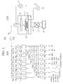
- FIG. 1 is a side view illustrating a constitution of a parallel plate plasma enhanced CVD apparatus 101 used for a method of manufacturing a semiconductor device according to an embodiment of the present invention.
- a high frequency electric power supply source (RF electric power supply source) 7 for supplying high frequency electric power of a frequency of 13.56 MHz is connected to the upper electrode 2.
- a low frequency electric power supply source 8 for supplying low frequency electric power of a frequency of 380 kHz is connected to the lower electrode 3.
- the high frequency electric power is supplied to the upper electrode 2 from at least the high frequency electric power supply source 7 of these power sources 7 and 8, and the film forming gas is converted to a plasma.
- the upper electrode 2, the lower electrode 3 and the power sources 7 and 8 constitute plasma generation means for converting the film forming gas into a plasma.
- These gases are suitably supplied to the chamber 1 in the film forming portion 101A through branch pipes 9b to 9i and the pipe 9a connected to the branch pipes 9b to 9i.
- branch pipes 9b to 9i there are provided flow rate adjusting means 11a to 11h and open/close means 10b to 10n and 10p to 10r for controlling communication/noncommunication of the branch pipes 9b to 9i.
- Open/close means 10a for opening/closing the pipe 9a is provided in the pipe 9a.
- FIG.19 is a sectional view of a semiconductor device in which the above film forming method is applied to a barrier insulating film covering a wiring made mainly of copper.
- films denoted by symbols 35a, 39 are the barrier insulating films covering a lower wiring and upper wiring made mainly of copper, respectively.
- a lower wiring berried insulating film 32, an inter wiring layer insulating film 35 and an upper wiring berried insulating film 36 on the substrate 31.
- the wiring berried insulating film 32, 36 both are formed of a low dielectric insulating film
- the inter wiring layer insulating film 35 is formed of a two-layered structure of the barrier insulating film and a low dielectric insulating film.
- an alkyl compound having a siloxane bond, methyl silane, an alkyl compound having an O-Si-O bond, and hydrocarbon which are the film forming gas of the barrier insulating film used for the present invention.
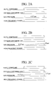
- FIG. 1 are charts illustrating a timing of an introductions of each gas composing the film forming gas into the chamber 1, conditions of a gas flow rate and gas pressure during the film formation, and a method of applying high frequency power and low frequency power applied to two electrodes of parallel plate type during the film formation.
- FIGs. 2A to 2E illustrates the charts of the method of forming a silicon-containing insulating film by use of a film forming gas composed of at least an alkyl compound and an oxygen-containing gas.
- the pressure of the film forming gas introduced into the chamber 1 is regulated to 1 Torr or less, and high frequency power is applied to any one of the lower and upper electrodes 2 and 3, thus converting the film forming gas into a plasma state.
- the chart of FIG. 2B differs from that of FIG. 2A in that the film formation is carried out while increasing the pressure of the film forming gas from low pressure to 1 Torr gradually.
- the chart of FIG. 2C differs from that of FIG. 2A in that the pressure of the film forming gas introduced into the chamber 1 is regulated to 1 Torr or less for a certain period of time at the early stage of the film formation, and then regulated to a higher pressure than 1 Torr after passage of the certain period of time.
- FIGs. 2F to 2K described below on the assumption that the gases shown in the drawings are composed by adding these gases to other gases, only conditions under which each of the gases is added to other gases are illustrated.
- FIGs. 2F to 2H are charts when the film formation is carried out by use of a film forming gas containing dilution gas.
- FIG. 2F the dilution gas of an ordinary flow rate is added.
- the chart of FIG. 2G differs from that of FIG. 2F in that the flow rate of the dilution gas is increased.
- the chart of FIG. 2H differs from that of FIG. 2F in that the flow rate of the dilution gas is increased for a certain period of time at the early stage of the film formation and, then, is lowered after passage of the certain period of time.
- the chart of FIG. 2I at least any one of the ammonium gas and the nitrogen gas is added through the entire period of the film formation.
- the chart of FIG. 2J differs from that of FIG. 2I in that at least any one of the ammonium gas and the nitrogen gas is supplied only for a certain period of time at the early stage of the film formation.
- the combinations of the gases illustrated in FIGS. 2F to 2K and other gases are realized by the following methods (a) to (c).
- (a) The gas of FIGs. 2B, 2D or 2E and any one of gases of FIGs. 2F to 2K can be combined.
- (b) The gas obtained by combining the gas of FIGs. 2B, 2D or 2E with any one of the gases of FIGs. 2F to 2H can be combined with any one of gases of FIGs. 2I to 2J.
- each gas obtained as a result of the combinations of (b) can be combined with the gas of FIG. 2K.
- the film forming gas which is converted into a plasma state only by the high frequency power, a low relative dielectric constant can be achieved. Furthermore, it is possible to maintain denseness of the insulating film enough to prevent copper diffusion by controlling the pressure of the film forming gas to 1 Torr or less at least at the early stage of the film formation.
- a dense film can be obtained at the portion closer to the wiring or the electrode mainly formed of the copper film, and a film with a lower dielectric constant can be obtained as the film is apart from the wiring or the electrode.
- the denseness can be enhanced by adding ammonium (NH 3 ) or nitrogen (N 2 ) to the film forming gas at least at the early stage of the film formation, or by using the film forming gas containing the dilution gas composed of He, or by using the film forming gas increasing the flow rate of the dilution gas at least at the early stage of the film formation, or by applying bias power of the low frequency at the early stage of the film formation.
- NH 3 ammonium
- N 2 nitrogen
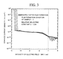
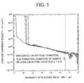
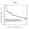
- the copper film was grounded and a negative voltage was applied to the mercury probe.
- the leakage current is nearly equal to 10 -10 A/cm 2 when the intensity of the electric field is -1 MV/cm. All over the measurement ranges of the electric field intensity, the leakage current hardly changes before and after the performance of annealing.
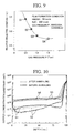
- FIG. 9 is the graph illustrating states of the change of the relative dielectric constant (k) of the insulating film relative to the gas pressure (P) of the film forming gas and the relationship of the dielectric breakdown-resistance of the insulating film after annealing with the gas pressure (P) and the relative dielectric constant (k).
- the ordinate indicates the relative dielectric constant (k) expressed by a linear scale
- the abscissa indicates the gas pressure (P) (Torr) of the film forming gas, which is expressed by a linear scale.
- the measurement points are expressed by the symbol ⁇ .
- the symbol ⁇ in the symbol ⁇ indicates that all of the five measurement samples are not broken during the dielectric breakdown-resistance test after annealing.
- the symbol X in the symbol ⁇ indicates that all of the five measurement samples are broken.
- the symbol ⁇ indicates that one or two measurement samples among the five measurement samples are broken.
- FIG. 10 is a graph illustrating investigation results of the barrier property of the formed insulating film for copper.
- the investigating results of FIG. 10 are obtained by investigating the copper distribution in the insulating film before and after annealing by use of SIMS.
- the ordinate indicates a copper concentration (arbitrary unit) in the insulating film, which is expressed by a logarithmic scale
- the abscissa indicates measurement spots (nm) measured from the surface of the insulating film, which are expressed by a linear scale.
- any of the samples S1 to S4 contains copper in its insulating film from the time when the samples S1 to S4 are subjected to annealing, and this is considered as that the insulating film is adulterated with the copper during the film formation. Accordingly, it is inevitable that the change of the content of the copper in the insulating film before and after annealing is observed based on FIG. 10.
- FIG 12 is a graph illustrating states of a change of a relative dielectric constant (k) of an insulating film relative to a He gas flow rate in a film forming gas, and a relationship of a dielectric breakdown-resistance of the insulating film after annealing with the He gas flow rate and the relative dielectric constant (k).
- the treatment conditions prior to the film formation and the annealing conditions are the same as those of the first embodiment.
- the film forming conditions are as follows.
- a seventh embodiment of the present invention will be described with reference to FIG. 13.
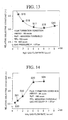
- FIG. 13 is a graph illustrating states of a change of a relative dielectric constant (k) of an insulating film relative to a N 2 O gas flow rate in a film forming gas and a relationship of a dielectric breakdown-resistance of the insulating film after annealing with the N 2 O gas flow rate and the relative dielectric constant (k).
- the seventh embodiment differs from the fifth embodiment (FIG.11) in that the film forming gas contains a NH 3 gas.
- the treatment conditions prior to the film formation and the annealing conditions are the same as those of the first embodiment.
- the film forming conditions are as follows.
- FIG. 14 is a graph illustrating states of a change of a relative dielectric constant (k) of an insulating film relative to a NH 3 gas flow rate in a film forming gas and a relationship of a dielectric breakdown-resistance of the insulating film after annealing with the NH 3 gas flow rate and the relative dielectric constant (k).
- the treatment conditions prior to the film formation and the annealing conditions are the same as those of the first embodiment.
- the film forming conditions are as follows.
- the dielectric breakdown-resistance is larger as the relative dielectric constant is higher. Therefore, it is difficult for the single layers composed of the insulating films according to the fourth to eighth embodiments to meet the demand for a low relative dielectric constant and a high dielectric breakdown-resistance.
- the insulating film is at least composed of two or more layers, in which an insulating film showing an excellent dielectric breakdown-resistance in spite of a high relative dielectric constant and an insulating film showing a low relative dielectric breakdown-resistance in spite of a low relative dielectric constant are stacked.
- an insulating film showing an excellent dielectric breakdown-resistance is made to be thin and an insulating film showing a low relative dielectric constant is made to be thick.
- the ninth embodiment differs from the fourth to eighth embodiments in that an insulating film composed of a underlying film (symbol ⁇ ) covering copper and a main insulating film (symbol ⁇ ) formed on the underlying film is formed.
- the thickness of the underlying film was set to 10 nm, and the thickness of the main insulating film was set to 90 nm.
- the dielectric breakdown-resistance of the entire two-layered structure formed of the two insulating films was investigated.
- FIG. 15 the sorts (L1 to L3) of the underlying films prepared by changing the gas pressure P are shown, and the relationship between the gas pressure P and the relative dielectric constant is shown.
- FIG. 16 the sorts (L4 and L5) of the underlying films prepared by changing the N 2 O gas flow rate are shown, and the relationship between the N 2 O gas flow rate and the relative dielectric constant is shown.
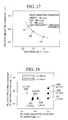
- FIG. 17 the sorts (U1 to U3) of the main insulating films prepared by changing the gas pressure P are shown, and the relationship between the gas pressure P and the relative dielectric constant is shown.
- FIG. 18 the results obtained by investigating the dielectric breakdown-resistance of the two-layered insulating film (S25 to S31) in which the underlying film of FIGs. 15 and 16 and the main insulating film of FIG. 17 are combined.
- FIG. 15 is a graph illustrating states of a change of the relative dielectric constant (k) of a underlying film relative to the gas pressure (P) of a film forming gas.
- the ordinate indicates the relative dielectric constant (k) expressed by a linear scale
- the abscissa indicates the gas pressure (P) (Torr) of the film forming gas, which is expressed by a linear scale.
- the treatment conditions prior to the film formation and the annealing conditions are the same as those of the first embodiment.
- the film forming conditions are as follows.
Landscapes
- Chemical & Material Sciences (AREA)
- Engineering & Computer Science (AREA)
- Metallurgy (AREA)
- Chemical Kinetics & Catalysis (AREA)
- Materials Engineering (AREA)
- Mechanical Engineering (AREA)
- General Chemical & Material Sciences (AREA)
- Organic Chemistry (AREA)
- Inorganic Chemistry (AREA)
- Physics & Mathematics (AREA)
- Plasma & Fusion (AREA)
- Internal Circuitry In Semiconductor Integrated Circuit Devices (AREA)
- Chemical Vapour Deposition (AREA)
- Formation Of Insulating Films (AREA)
Applications Claiming Priority (4)
| Application Number | Priority Date | Filing Date | Title |
|---|---|---|---|
| JP2001372299 | 2001-12-06 | ||
| JP2001372299 | 2001-12-06 | ||
| JP2002127388A JP3701626B2 (ja) | 2001-12-06 | 2002-04-26 | 半導体装置の製造方法 |
| JP2002127388 | 2002-04-26 |
Publications (2)
| Publication Number | Publication Date |
|---|---|
| EP1321976A2 true EP1321976A2 (fr) | 2003-06-25 |
| EP1321976A3 EP1321976A3 (fr) | 2004-11-17 |
Family
ID=26624900
Family Applications (1)
| Application Number | Title | Priority Date | Filing Date |
|---|---|---|---|
| EP02024920A Withdrawn EP1321976A3 (fr) | 2001-12-06 | 2002-11-06 | Procédé de dépôt d'une couche barrière isolante à faible constante diélectrique sur une couche de cuivre |
Country Status (5)
| Country | Link |
|---|---|
| US (1) | US6780790B2 (fr) |
| EP (1) | EP1321976A3 (fr) |
| JP (1) | JP3701626B2 (fr) |
| KR (1) | KR100546958B1 (fr) |
| TW (1) | TWI274380B (fr) |
Cited By (3)
| Publication number | Priority date | Publication date | Assignee | Title |
|---|---|---|---|---|
| WO2004038783A3 (fr) * | 2002-10-21 | 2004-05-27 | Massachusetts Inst Technology | Depot chimique en phase vapeur de films minces d'organosilicate |
| WO2004111296A3 (fr) * | 2003-06-12 | 2005-05-06 | Applied Materials Inc | Reduction de contrainte dans un film de sioc a faible constante dielectrique (k) par addition d'alkylenes a des processus a base d'omct |
| US7112615B2 (en) | 2002-07-22 | 2006-09-26 | Massachusetts Institute Of Technology | Porous material formation by chemical vapor deposition onto colloidal crystal templates |
Families Citing this family (19)
| Publication number | Priority date | Publication date | Assignee | Title |
|---|---|---|---|---|
| US20030211244A1 (en) * | 2002-04-11 | 2003-11-13 | Applied Materials, Inc. | Reacting an organosilicon compound with an oxidizing gas to form an ultra low k dielectric |
| US20030194495A1 (en) * | 2002-04-11 | 2003-10-16 | Applied Materials, Inc. | Crosslink cyclo-siloxane compound with linear bridging group to form ultra low k dielectric |
| US7056560B2 (en) * | 2002-05-08 | 2006-06-06 | Applies Materials Inc. | Ultra low dielectric materials based on hybrid system of linear silicon precursor and organic porogen by plasma-enhanced chemical vapor deposition (PECVD) |
| US7060330B2 (en) * | 2002-05-08 | 2006-06-13 | Applied Materials, Inc. | Method for forming ultra low k films using electron beam |
| US6936551B2 (en) * | 2002-05-08 | 2005-08-30 | Applied Materials Inc. | Methods and apparatus for E-beam treatment used to fabricate integrated circuit devices |
| US6897163B2 (en) * | 2003-01-31 | 2005-05-24 | Applied Materials, Inc. | Method for depositing a low dielectric constant film |
| US20050037153A1 (en) * | 2003-08-14 | 2005-02-17 | Applied Materials, Inc. | Stress reduction of sioc low k films |
| US20050214457A1 (en) * | 2004-03-29 | 2005-09-29 | Applied Materials, Inc. | Deposition of low dielectric constant films by N2O addition |
| US7740704B2 (en) | 2004-06-25 | 2010-06-22 | Tokyo Electron Limited | High rate atomic layer deposition apparatus and method of using |
| US8039049B2 (en) * | 2005-09-30 | 2011-10-18 | Tokyo Electron Limited | Treatment of low dielectric constant films using a batch processing system |
| JP4684866B2 (ja) * | 2005-11-17 | 2011-05-18 | ルネサスエレクトロニクス株式会社 | 半導体装置の製造方法 |
| JP5093479B2 (ja) * | 2005-11-24 | 2012-12-12 | 日本電気株式会社 | 多孔質絶縁膜の形成方法 |
| US20070134435A1 (en) * | 2005-12-13 | 2007-06-14 | Ahn Sang H | Method to improve the ashing/wet etch damage resistance and integration stability of low dielectric constant films |
| US7297376B1 (en) | 2006-07-07 | 2007-11-20 | Applied Materials, Inc. | Method to reduce gas-phase reactions in a PECVD process with silicon and organic precursors to deposit defect-free initial layers |
| US7964442B2 (en) * | 2007-10-09 | 2011-06-21 | Applied Materials, Inc. | Methods to obtain low k dielectric barrier with superior etch resistivity |
| JP2009177023A (ja) * | 2008-01-25 | 2009-08-06 | Nec Corp | 多孔質絶縁膜及びその形成方法並びに半導体装置の製造方法 |
| JP2011155077A (ja) * | 2010-01-26 | 2011-08-11 | Renesas Electronics Corp | 半導体装置の製造方法 |
| US8741394B2 (en) * | 2010-03-25 | 2014-06-03 | Novellus Systems, Inc. | In-situ deposition of film stacks |
| US8461683B2 (en) * | 2011-04-01 | 2013-06-11 | Intel Corporation | Self-forming, self-aligned barriers for back-end interconnects and methods of making same |
Family Cites Families (21)
| Publication number | Priority date | Publication date | Assignee | Title |
|---|---|---|---|---|
| US5040046A (en) | 1990-10-09 | 1991-08-13 | Micron Technology, Inc. | Process for forming highly conformal dielectric coatings in the manufacture of integrated circuits and product produced thereby |
| DE69130947T2 (de) | 1991-01-08 | 1999-07-08 | Fujitsu Ltd., Kawasaki, Kanagawa | Verfahren zur bildung eines siliciumoxid-filmes |
| JP2684942B2 (ja) | 1992-11-30 | 1997-12-03 | 日本電気株式会社 | 化学気相成長法と化学気相成長装置および多層配線の製造方法 |
| JP2899600B2 (ja) * | 1994-01-25 | 1999-06-02 | キヤノン販売 株式会社 | 成膜方法 |
| JPH098032A (ja) * | 1995-06-20 | 1997-01-10 | Sony Corp | 絶縁膜形成方法 |
| JP3226479B2 (ja) * | 1996-08-29 | 2001-11-05 | 松下電器産業株式会社 | 層間絶縁膜の形成方法 |
| KR100205318B1 (ko) * | 1996-10-11 | 1999-07-01 | 구본준 | 자유전율의 절연막 제조방법 |
| AU7371898A (en) | 1997-05-07 | 1998-11-27 | Mark J. Hampden-Smith | Low density film for low dielectric constant applications |
| JPH113888A (ja) | 1997-05-28 | 1999-01-06 | Texas Instr Inc <Ti> | 集積回路誘電体及び方法 |
| US6051321A (en) | 1997-10-24 | 2000-04-18 | Quester Technology, Inc. | Low dielectric constant materials and method |
| JP3726226B2 (ja) | 1998-02-05 | 2005-12-14 | 日本エー・エス・エム株式会社 | 絶縁膜及びその製造方法 |
| US6287990B1 (en) | 1998-02-11 | 2001-09-11 | Applied Materials, Inc. | CVD plasma assisted low dielectric constant films |
| JP2000058544A (ja) * | 1998-08-04 | 2000-02-25 | Matsushita Electron Corp | 半導体装置及びその製造方法 |
| JP3197007B2 (ja) * | 1999-06-08 | 2001-08-13 | 日本エー・エス・エム株式会社 | 半導体基板上のシリコン重合体絶縁膜及びその膜を形成する方法 |
| JP3348084B2 (ja) * | 1999-12-28 | 2002-11-20 | キヤノン販売株式会社 | 成膜方法及び半導体装置 |
| JP3419745B2 (ja) * | 2000-02-28 | 2003-06-23 | キヤノン販売株式会社 | 半導体装置及びその製造方法 |
| JP2001291713A (ja) * | 2000-04-07 | 2001-10-19 | Canon Sales Co Inc | 成膜方法及び半導体装置 |
| US6410462B1 (en) * | 2000-05-12 | 2002-06-25 | Sharp Laboratories Of America, Inc. | Method of making low-K carbon doped silicon oxide |
| JP3600507B2 (ja) * | 2000-05-18 | 2004-12-15 | キヤノン販売株式会社 | 半導体装置及びその製造方法 |
| JP3532830B2 (ja) * | 2000-05-24 | 2004-05-31 | キヤノン販売株式会社 | 半導体装置及びその製造方法 |
| JP2003100148A (ja) * | 2001-09-25 | 2003-04-04 | Jsr Corp | 膜形成方法、絶縁膜および半導体用基板 |
-
2002
- 2002-04-26 JP JP2002127388A patent/JP3701626B2/ja not_active Expired - Fee Related
- 2002-11-05 US US10/287,549 patent/US6780790B2/en not_active Expired - Lifetime
- 2002-11-05 TW TW091132588A patent/TWI274380B/zh not_active IP Right Cessation
- 2002-11-06 EP EP02024920A patent/EP1321976A3/fr not_active Withdrawn
- 2002-11-25 KR KR1020020073587A patent/KR100546958B1/ko not_active Expired - Fee Related
Cited By (3)
| Publication number | Priority date | Publication date | Assignee | Title |
|---|---|---|---|---|
| US7112615B2 (en) | 2002-07-22 | 2006-09-26 | Massachusetts Institute Of Technology | Porous material formation by chemical vapor deposition onto colloidal crystal templates |
| WO2004038783A3 (fr) * | 2002-10-21 | 2004-05-27 | Massachusetts Inst Technology | Depot chimique en phase vapeur de films minces d'organosilicate |
| WO2004111296A3 (fr) * | 2003-06-12 | 2005-05-06 | Applied Materials Inc | Reduction de contrainte dans un film de sioc a faible constante dielectrique (k) par addition d'alkylenes a des processus a base d'omct |
Also Published As
| Publication number | Publication date |
|---|---|
| JP3701626B2 (ja) | 2005-10-05 |
| KR100546958B1 (ko) | 2006-01-31 |
| EP1321976A3 (fr) | 2004-11-17 |
| TW200300965A (en) | 2003-06-16 |
| US6780790B2 (en) | 2004-08-24 |
| TWI274380B (en) | 2007-02-21 |
| US20030109136A1 (en) | 2003-06-12 |
| KR20030047735A (ko) | 2003-06-18 |
| JP2003234346A (ja) | 2003-08-22 |
Similar Documents
| Publication | Publication Date | Title |
|---|---|---|
| US6780790B2 (en) | Semiconductor device and method of manufacturing the same | |
| KR100494480B1 (ko) | 반도체 장치의 제조 방법 | |
| KR100407012B1 (ko) | 반도체 장치 및 그 제조 방법 | |
| US6852651B2 (en) | Semiconductor device and method of manufacturing the same | |
| JP3745257B2 (ja) | 半導体装置及びその製造方法 | |
| JP3600507B2 (ja) | 半導体装置及びその製造方法 | |
| EP1211728A2 (fr) | Dispositif semi-conducteur et procédé pour sa fabrication | |
| US6673725B2 (en) | Semiconductor device and method of manufacturing the same | |
| US6630412B2 (en) | Semiconductor device and method of manufacturing the same | |
| JP2005294333A (ja) | 成膜方法及び半導体装置 | |
| KR20020009440A (ko) | 성막 방법, 반도체 장치 및 그 제조 방법 | |
| EP1247876A2 (fr) | Procédé de fabrication d'un dispositif semiconducteur | |
| EP1128421A2 (fr) | Méthode de fabrication d'une d'une couche isolante intermédiaire contenant les éléments Si, C, O et H pour composants semiconducteurs | |
| JP2004200713A (ja) | 半導体装置及びその製造方法 |
Legal Events
| Date | Code | Title | Description |
|---|---|---|---|
| PUAI | Public reference made under article 153(3) epc to a published international application that has entered the european phase |
Free format text: ORIGINAL CODE: 0009012 |
|
| AK | Designated contracting states |
Designated state(s): AT BE BG CH CY CZ DE DK EE ES FI FR GB GR IE IT LI LU MC NL PT SE SK TR |
|
| AX | Request for extension of the european patent |
Extension state: AL LT LV MK RO SI |
|
| PUAL | Search report despatched |
Free format text: ORIGINAL CODE: 0009013 |
|
| AK | Designated contracting states |
Kind code of ref document: A3 Designated state(s): AT BE BG CH CY CZ DE DK EE ES FI FR GB GR IE IT LI LU MC NL PT SE SK TR |
|
| AX | Request for extension of the european patent |
Extension state: AL LT LV MK RO SI |
|
| 17P | Request for examination filed |
Effective date: 20050104 |
|
| AKX | Designation fees paid |
Designated state(s): DE FR GB NL |
|
| STAA | Information on the status of an ep patent application or granted ep patent |
Free format text: STATUS: THE APPLICATION IS DEEMED TO BE WITHDRAWN |
|
| 18D | Application deemed to be withdrawn |
Effective date: 20060818 |