EP1321982A2 - Procédé de brasage direct sur des plages de cuivre dans des circuits intégrés au niveau de plaquettes - Google Patents
Procédé de brasage direct sur des plages de cuivre dans des circuits intégrés au niveau de plaquettes Download PDFInfo
- Publication number
- EP1321982A2 EP1321982A2 EP02102839A EP02102839A EP1321982A2 EP 1321982 A2 EP1321982 A2 EP 1321982A2 EP 02102839 A EP02102839 A EP 02102839A EP 02102839 A EP02102839 A EP 02102839A EP 1321982 A2 EP1321982 A2 EP 1321982A2
- Authority
- EP
- European Patent Office
- Prior art keywords
- copper
- layer
- wafer
- overcoat
- metallization
- Prior art date
- Legal status (The legal status is an assumption and is not a legal conclusion. Google has not performed a legal analysis and makes no representation as to the accuracy of the status listed.)
- Granted
Links
Images
Classifications
-
- H—ELECTRICITY
- H10—SEMICONDUCTOR DEVICES; ELECTRIC SOLID-STATE DEVICES NOT OTHERWISE PROVIDED FOR
- H10W—GENERIC PACKAGES, INTERCONNECTIONS, CONNECTORS OR OTHER CONSTRUCTIONAL DETAILS OF DEVICES COVERED BY CLASS H10
- H10W72/00—Interconnections or connectors in packages
- H10W72/20—Bump connectors, e.g. solder bumps or copper pillars; Dummy bumps; Thermal bumps
-
- H—ELECTRICITY
- H10—SEMICONDUCTOR DEVICES; ELECTRIC SOLID-STATE DEVICES NOT OTHERWISE PROVIDED FOR
- H10W—GENERIC PACKAGES, INTERCONNECTIONS, CONNECTORS OR OTHER CONSTRUCTIONAL DETAILS OF DEVICES COVERED BY CLASS H10
- H10W72/00—Interconnections or connectors in packages
- H10W72/01—Manufacture or treatment
- H10W72/012—Manufacture or treatment of bump connectors, dummy bumps or thermal bumps
- H10W72/01221—Manufacture or treatment of bump connectors, dummy bumps or thermal bumps using local deposition
- H10W72/01223—Manufacture or treatment of bump connectors, dummy bumps or thermal bumps using local deposition in liquid form, e.g. by dispensing droplets or by screen printing
-
- H—ELECTRICITY
- H10—SEMICONDUCTOR DEVICES; ELECTRIC SOLID-STATE DEVICES NOT OTHERWISE PROVIDED FOR
- H10W—GENERIC PACKAGES, INTERCONNECTIONS, CONNECTORS OR OTHER CONSTRUCTIONAL DETAILS OF DEVICES COVERED BY CLASS H10
- H10W72/00—Interconnections or connectors in packages
- H10W72/01—Manufacture or treatment
- H10W72/012—Manufacture or treatment of bump connectors, dummy bumps or thermal bumps
- H10W72/01251—Changing the shapes of bumps
- H10W72/01255—Changing the shapes of bumps by using masks
-
- H—ELECTRICITY
- H10—SEMICONDUCTOR DEVICES; ELECTRIC SOLID-STATE DEVICES NOT OTHERWISE PROVIDED FOR
- H10W—GENERIC PACKAGES, INTERCONNECTIONS, CONNECTORS OR OTHER CONSTRUCTIONAL DETAILS OF DEVICES COVERED BY CLASS H10
- H10W72/00—Interconnections or connectors in packages
- H10W72/01—Manufacture or treatment
- H10W72/019—Manufacture or treatment of bond pads
- H10W72/01971—Cleaning, e.g. oxide removal
-
- H—ELECTRICITY
- H10—SEMICONDUCTOR DEVICES; ELECTRIC SOLID-STATE DEVICES NOT OTHERWISE PROVIDED FOR
- H10W—GENERIC PACKAGES, INTERCONNECTIONS, CONNECTORS OR OTHER CONSTRUCTIONAL DETAILS OF DEVICES COVERED BY CLASS H10
- H10W72/00—Interconnections or connectors in packages
- H10W72/20—Bump connectors, e.g. solder bumps or copper pillars; Dummy bumps; Thermal bumps
- H10W72/221—Structures or relative sizes
-
- H—ELECTRICITY
- H10—SEMICONDUCTOR DEVICES; ELECTRIC SOLID-STATE DEVICES NOT OTHERWISE PROVIDED FOR
- H10W—GENERIC PACKAGES, INTERCONNECTIONS, CONNECTORS OR OTHER CONSTRUCTIONAL DETAILS OF DEVICES COVERED BY CLASS H10
- H10W72/00—Interconnections or connectors in packages
- H10W72/20—Bump connectors, e.g. solder bumps or copper pillars; Dummy bumps; Thermal bumps
- H10W72/251—Materials
-
- H—ELECTRICITY
- H10—SEMICONDUCTOR DEVICES; ELECTRIC SOLID-STATE DEVICES NOT OTHERWISE PROVIDED FOR
- H10W—GENERIC PACKAGES, INTERCONNECTIONS, CONNECTORS OR OTHER CONSTRUCTIONAL DETAILS OF DEVICES COVERED BY CLASS H10
- H10W72/00—Interconnections or connectors in packages
- H10W72/20—Bump connectors, e.g. solder bumps or copper pillars; Dummy bumps; Thermal bumps
- H10W72/251—Materials
- H10W72/252—Materials comprising solid metals or solid metalloids, e.g. PbSn, Ag or Cu
-
- H—ELECTRICITY
- H10—SEMICONDUCTOR DEVICES; ELECTRIC SOLID-STATE DEVICES NOT OTHERWISE PROVIDED FOR
- H10W—GENERIC PACKAGES, INTERCONNECTIONS, CONNECTORS OR OTHER CONSTRUCTIONAL DETAILS OF DEVICES COVERED BY CLASS H10
- H10W72/00—Interconnections or connectors in packages
- H10W72/20—Bump connectors, e.g. solder bumps or copper pillars; Dummy bumps; Thermal bumps
- H10W72/29—Bond pads specially adapted therefor
-
- H—ELECTRICITY
- H10—SEMICONDUCTOR DEVICES; ELECTRIC SOLID-STATE DEVICES NOT OTHERWISE PROVIDED FOR
- H10W—GENERIC PACKAGES, INTERCONNECTIONS, CONNECTORS OR OTHER CONSTRUCTIONAL DETAILS OF DEVICES COVERED BY CLASS H10
- H10W72/00—Interconnections or connectors in packages
- H10W72/50—Bond wires
- H10W72/551—Materials of bond wires
- H10W72/552—Materials of bond wires comprising metals or metalloids, e.g. silver
- H10W72/5522—Materials of bond wires comprising metals or metalloids, e.g. silver comprising gold [Au]
-
- H—ELECTRICITY
- H10—SEMICONDUCTOR DEVICES; ELECTRIC SOLID-STATE DEVICES NOT OTHERWISE PROVIDED FOR
- H10W—GENERIC PACKAGES, INTERCONNECTIONS, CONNECTORS OR OTHER CONSTRUCTIONAL DETAILS OF DEVICES COVERED BY CLASS H10
- H10W72/00—Interconnections or connectors in packages
- H10W72/50—Bond wires
- H10W72/59—Bond pads specially adapted therefor
-
- H—ELECTRICITY
- H10—SEMICONDUCTOR DEVICES; ELECTRIC SOLID-STATE DEVICES NOT OTHERWISE PROVIDED FOR
- H10W—GENERIC PACKAGES, INTERCONNECTIONS, CONNECTORS OR OTHER CONSTRUCTIONAL DETAILS OF DEVICES COVERED BY CLASS H10
- H10W72/00—Interconnections or connectors in packages
- H10W72/90—Bond pads, in general
- H10W72/951—Materials of bond pads
- H10W72/952—Materials of bond pads comprising metals or metalloids, e.g. PbSn, Ag or Cu
Definitions
- the present invention is related in general to the field of semiconductor devices and processes and more specifically to the structure and fabrication method of metal bumps for flip-chip assembly of semiconductor chips.
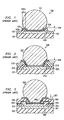
- FIG. 1 illustrates schematically an example of the metallurgical requirements in known technology for a contact pad of a small portion of an IC chip generally designated 100.
- a semiconductor material 101 typically silicon, has patterned aluminum metallization 102 and is protected by a dielectric, moisture-impermeable protective overcoat 103, usually silicon nitride or oxynitride.
- a window has been opened in the overcoat 103 to expose metallization 102 and leave a protective perimeter 103a around metallization 102.
- An additional "under bump" metallization 104 has been deposited unto metallization 102 and patterned so that it overlaps by a distance 104a over the overcoat 103. This additional metallization 104 usually consists of a sequence of thin layers.
- the bottom layer is typically a refractory metal 105, such as chromium, titanium, or tungsten, which provides an ohmic contact to aluminum 102 and a moisture-impenetrable interface to overcoat 103.
- the top metal 106 has to be solderable; examples are gold, copper, nickel, or palladium.
- solder material is deposited, commonly by evaporation, plating or screen-printing, and reflown to form bump 107. These solder bumps assume various shapes (examples are semi-spheres, domes and truncated balls) after the reflow process, influenced by the forces of surface tension during the reflow process.
- One method aims at absorbing part of the thermomechanical stress on the solder joints by plastic material surrounding the joints and filling the gap between chip and substrate. See for instance, U. S. Patents # 6,228,680, issued on May 8, 2001; # 6,213,347, issued on Apr. 10, 2001, and # 6,245,583, issued on Jun. 12, 2001 (Thomas et al., Low Stress Method and Apparatus for Underfilling Flip-Chip Electronic Devices).
- the underfilling method represents an unwelcome process step after device attachment to the motherboard.
- Another method applies a polymer layer on top of the protective overcoat with the aim of reducing the stress to the overcoat perimeter and the dielectric material underlying the contact pad. See for instance the publication "A Silicon and Aluminum Dynamic Memory Technology” by Richard A. Larsen (IBM J. Res. Develop., vol.24, May 1980, pp. 268-282).
- the article includes description of a flip-chip packaging technology using a solder bump on an under-bump metallization, which is resting its perimeter on a thick polyimide layer. The bump structure is often supported by another polyimide layer.
- FIG. 2 illustrates schematically an example of a contact pad, generally designated 200, including a polymer overcoat.
- a silicon chip 201 has patterned aluminum metallization 202 and is protected by a moisture-impermeable inorganic overcoat 203 (silicon nitride) and a polymeric layer 210 (benzocyclobutene or polyimide).
- a window has been opened through both overcoats.
- Layers of under-bump metallization 204 establishes contact to the aluminum, adhesion to both overcoats, and solderablilty to the solder bump 207.
- a structure and a fabrication method are described for metallurgical connections between solder bumps and contact pads positioned on integrated circuits (IC) having copper interconnecting metallization protected by an overcoat.
- the structure comprises a portion of the copper metallization exposed by a window in the overcoat, where the exposed copper has a chemically and plasma cleaned surface.
- a copper layer is directly positioned on the clean copper metallization, and patterned; the resulting metal structure has an electrical (and thermal) conductivity about equal to the conductivity of pure copper.
- the copper layer overlaps the perimeter of the overcoat window and a copper stud is positioned on said copper layer. Finally, one of the solder bumps is bonded to the copper stud.
- the present invention is related to high density and high speed ICs with copper interconnecting metallization, especially those having high numbers of metallized inputs/outputs for flip-chip assembly.
- These circuits can be found in many device families such as processors, digital and analog devices, logic devices, high frequency and high power devices, and in both large and small area chip categories.
- the present invention helps to alleviate the space constraint of continually shrinking applications such as cellular communication, pagers, hard disk drives, laptop computers and other portable electronic devices.
- Another aspect of the invention is to fabricate the contact pad copper cap-layer directly on the IC copper metallization without any intermediate barrier layer, so that the resulting minimum electrical resistance enhances the high speed performance of the IC.
- Another aspect of the invention is the flexibility to select the copper stud deposition method from the following options:
- Another aspect of the invention is to advance the process and reliability of wafer-level functional probing by eliminating probe marks and subsequent plating difficulties.
- Another object of the invention is to provide design and process concepts which are flexible so that they can be applied to many families of semiconductor products, and are general so that they can be applied to several generations of products.
- Another object of the invention is to use only designs and processes most commonly employed and accepted in the fabrication of IC devices, thus avoiding the cost of new capital investment and using the installed fabrication equipment base.
- an oxygen plasma removes organic residues; a subsequent first hydrogen-based plasma removes the controlled copper oxide and passivates the copper surface.
- Sputter etching then creates a fresh copper surface, onto which a copper layer is sputter deposited.
- a second hydrogen plasma passivates the surface. The plating of the copper stud completes the fabrication process.
- the copper layer is sputter-deposited without breaking the vacuum after the first hydrogen plasma.
- the wet clean and second hydrogen plasma can thus be omitted.
- a step of etching in an aqueous inorganic or organic acid is added between the steps of oxygen plasma and hydrogen plasma, in order to remove deep copper pad defects.
- Copper has to be shielded from diffusing into the silicon base material of the ICs in order to protect the circuits from the carrier lifetime killing characteristic of copper atoms positioned in the silicon lattice.
- the formation of thin copper(I)oxide films during the manufacturing process flow has to be prevented or corrected, since these films severely inhibit reliable attachment of solder bumps.
- bare copper bond pads are susceptible to corrosion.
- FIG. 3 illustrates an example emulating the example in FIG. 2.
- the top copper layer 301 of the IC is located over insulating material 302 and protected by inorganic overcoat 303 (usually silicon nitride).
- inorganic overcoat 303 usually silicon nitride.
- a first window is opened in overcoat 303 to expose a portion of copper metal 301.
- An aluminum cap 304 is deposited over the exposed copper 301, slightly overlapping the first window perimeter of overcoat 303.
- An additional pad nitride layer 305 and a polymeric overcoat 306 protect the aluminum 304.
- a second window is opened in pad nitride 305 and polymeric overcoat 306, forming a slope 306a and exposing portion of the aluminum layer 304.
- One, two or more barrier layers 307 are deposited over the exposed aluminum, similar to FIG. 2. The top barrier metal is solderable and contacted by solder bump 308.
- the described approach has several shortcomings.
- Third, the aluminum used for the cap is soft and thus gets severely damaged by the markings of the multiprobe contacts in electrical testing. This damage, in turn, becomes so dominant in the ever decreasing size of the contact pads that the subsequent barrier deposition becomes problematic.
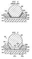
- FIG. 4 Another approach in known technology to overcome the solder attachment problems for copper metallization is depicted in FIG. 4.
- the top copper layer 401 of the IC is located over insulating material 402 and protected by inorganic overcoat 403 (usually silicon nitride) and polymeric overcoat 406.
- a window is opened in both overcoats 403 and 406, forming a slope 406a and exposing a portion of copper metal 401.
- a first barrier layer 407a selected from titanium, tantalum, tungsten, and alloys thereof, is deposited over the exposed copper 401 with the intent to establish good ohmic contact to the copper by "gettering" the oxide away from the copper.
- a second barrier layer 407b commonly nickel vanadium, is deposited to prevent outdiffusion of copper.
- solder bump 408 proceeds directly to screen printing the solder bump 408.
- Another process first sputters a copper seed layer and then electroplates a copper stud; finally, the solder bump is electroplated.
- the result is a contact pad with a high electrical resistance as determined by the resistance of the barrier metal layers. This high electrical pad resistance is counterproductive to the effort aiming at high speed ICs.
- the schematic cross section of FIG. 5 illustrates a metal structure for a contact pad, generally designated 500, of an IC having copper interconnecting metallization.
- the top copper layer 501 of the IC is located over insulating material 502 and protected by inorganic overcoat 503 and polymeric overcoat 506.
- the inorganic overcoat 503 consists preferably of moisture-impermeable silicon nitride, silicon oxynitride, silicon carbide, or multi-layers thereof, preferably in the thickness range from 0.5 to 2.5 ⁇ m.
- the organic overcoat 506 consists preferably of polyimide, benzocyclobutene or related materials, preferably in the thickness range from 3.0 to 10.0 ⁇ m.
- Overcoat 503 overlaps the copper 501 by a length 503a.
- the prime function of this organic material is to help absorb thermomechanical stress transferred by the solder bumps after completion of the device assembly on outside parts such as wiring boards.
- Overcoat 503 and especially the thicker overcoat 506 exhibit a slope 506a towards copper layer 501, brought about by the etching of the overcoats during the window opening process for exposing copper 501.
- the surface 501b of the exposed copper is carefully cleaned; see the process detail below. It is of pivotal importance to the present invention that the cleaned copper surface 501b is free of copper oxide, organic residues, or any contamination so that the interface of copper 501 to the copper layer 507 contributes no measurable electrical resistance to the resistance of contact pad 500.
- the copper layer 507 (deposition techniques see below) is patterned to overlay copper surface 501b and overcoat slope 506a; the preferred thickness range of copper layer 507 is from about 0.3 to 0.8 ⁇ m. Without any contamination of copper layer 507, copper stud 508 is deposited (various deposition methods see below).
- the stud has a thickness from about 10 to 20 ⁇ m; its width is equal to the extent of copper layer 507, following the contour of the overcoat slope 506a. There is no longer a need for any barrier layer as in the prior art depicted in FIGs. 1 to 4.
- the structure consisting of copper stud 508, copper layer 507, and copper metallization 501 exhibits the electrical (and thermal) conductivity of pure copper and thus the lowest possible electrical resistance for contact pad 500.
- solder bump 509 The metallurgical contact pad structure for a flip - chip IC is completed by depositing a solder bump 509; deposition methods see below.
- Preferred solder materials include tin, indium, tin/indium, tin/silver, tin/bismuth, conductive adhesives, and z-axis conductive materials. For some applications, the conventional tin/lead alloy may still be acceptable.
- electroplating is chosen as the method of depositing the copper stud 508
- electroplating is the preferred method of depositing solder bumps 509. This method allows small-pitch solder bumps.
- electroless plating is chosen as the method of depositing the copper stud, screen printing is preferred for the solder bumps; alternatively, pre-fabricated solder balls may be selected. These options require somewhat larger bump pitch.
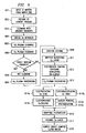
- FIG. 6 shows a block diagram of the preferred wafer-level process flow for direct bumping on copper pads according to the invention.
- the copper layer is sputter-deposited without breaking the vacuum after the first hydrogen plasma.
- the second wet clean and second hydrogen plasma can thus be omitted.
- a step of etching in an aqueous inorganic or organic acid is added between the steps of oxygen plasma and hydrogen plasma, in order to remove deep copper pad defects.
- the invention can be applied to IC bond pad metallizations other than copper, which are difficult or impossible to contact by conventional tin or solder techniques, such as alloys of refractory metals and noble metals.
- the invention can be extended to batch processing, further reducing fabrication costs.
- the invention can be used in hybrid technologies of wire/ribbon bonding and solder interconnections. It is therefore intended that the appended claims encompass any such modifications or embodiments.
Landscapes
- Wire Bonding (AREA)
- Internal Circuitry In Semiconductor Integrated Circuit Devices (AREA)
Applications Claiming Priority (4)
| Application Number | Priority Date | Filing Date | Title |
|---|---|---|---|
| US34294901P | 2001-12-21 | 2001-12-21 | |
| US342949 | 2001-12-21 | ||
| US10/086,117 US20030116845A1 (en) | 2001-12-21 | 2002-02-26 | Waferlevel method for direct bumping on copper pads in integrated circuits |
| US86117 | 2002-02-26 |
Publications (3)
| Publication Number | Publication Date |
|---|---|
| EP1321982A2 true EP1321982A2 (fr) | 2003-06-25 |
| EP1321982A3 EP1321982A3 (fr) | 2009-07-29 |
| EP1321982B1 EP1321982B1 (fr) | 2011-07-27 |
Family
ID=26774381
Family Applications (1)
| Application Number | Title | Priority Date | Filing Date |
|---|---|---|---|
| EP02102839A Expired - Lifetime EP1321982B1 (fr) | 2001-12-21 | 2002-12-19 | Procédé de fabrication à l'échelle d'une tranche d'une couche de cuivre revêtant un plot de connexion |
Country Status (2)
| Country | Link |
|---|---|
| US (2) | US20030116845A1 (fr) |
| EP (1) | EP1321982B1 (fr) |
Cited By (4)
| Publication number | Priority date | Publication date | Assignee | Title |
|---|---|---|---|---|
| DE102005035771A1 (de) * | 2005-07-29 | 2007-02-01 | Advanced Micro Devices, Inc., Sunnyvale | Technik zur Herstellung einer Kontaktschicht auf Kupferbasis ohne ein Endmetall |
| DE102008020924A1 (de) * | 2008-04-25 | 2009-11-05 | Siemens Aktiengesellschaft | Modul mit Niedertemperatur-Lötverbindung und dazugehöriges Verfahren zur Herstellung |
| CN103794513A (zh) * | 2012-10-26 | 2014-05-14 | 中国科学院上海微系统与信息技术研究所 | 增强介质层PI和金属Cu层之间粘附性的方法 |
| CN105633043A (zh) * | 2014-11-03 | 2016-06-01 | 中芯国际集成电路制造(上海)有限公司 | 一种半导体器件及其制造方法、电子装置 |
Families Citing this family (30)
| Publication number | Priority date | Publication date | Assignee | Title |
|---|---|---|---|---|
| JP2003198117A (ja) * | 2001-12-28 | 2003-07-11 | Matsushita Electric Ind Co Ltd | はんだ付け方法および接合構造体 |
| TW513770B (en) * | 2002-02-26 | 2002-12-11 | Advanced Semiconductor Eng | Wafer bumping process |
| US20040036171A1 (en) * | 2002-08-22 | 2004-02-26 | Farnworth Warren M. | Method and apparatus for enabling a stitch wire bond in the absence of discrete bump formation, semiconductor device assemblies and electronic systems including same |
| US6964881B2 (en) * | 2002-08-27 | 2005-11-15 | Micron Technology, Inc. | Multi-chip wafer level system packages and methods of forming same |
| TWI291210B (en) * | 2002-09-10 | 2007-12-11 | Advanced Semiconductor Eng | Under-bump-metallurgy layer |
| US7138293B2 (en) * | 2002-10-04 | 2006-11-21 | Dalsa Semiconductor Inc. | Wafer level packaging technique for microdevices |
| JP4591084B2 (ja) * | 2002-12-09 | 2010-12-01 | 日本電気株式会社 | 配線用銅合金、半導体装置及び半導体装置の製造方法 |
| US7095116B1 (en) * | 2003-12-01 | 2006-08-22 | National Semiconductor Corporation | Aluminum-free under bump metallization structure |
| JP4352880B2 (ja) * | 2003-12-02 | 2009-10-28 | セイコーエプソン株式会社 | 洗浄方法および洗浄装置 |
| KR100605315B1 (ko) | 2004-07-30 | 2006-07-28 | 삼성전자주식회사 | 집적회로 칩의 입출력 패드 구조 |
| TWI251890B (en) * | 2004-11-05 | 2006-03-21 | Advanced Semiconductor Eng | Wafer structure, chip structure and bumping process |
| US7282433B2 (en) * | 2005-01-10 | 2007-10-16 | Micron Technology, Inc. | Interconnect structures with bond-pads and methods of forming bump sites on bond-pads |
| US7323406B2 (en) | 2005-01-27 | 2008-01-29 | Chartered Semiconductor Manufacturing Ltd. | Elevated bond-pad structure for high-density flip-clip packaging and a method of fabricating the structures |
| KR100630737B1 (ko) * | 2005-02-04 | 2006-10-02 | 삼성전자주식회사 | 금속 cmp 후 세정액 및 이를 이용한 반도체 소자의금속 배선 형성 방법 |
| TWI245345B (en) * | 2005-02-17 | 2005-12-11 | Touch Micro System Tech | Method of forming a wear-resistant dielectric layer |
| CN100437936C (zh) * | 2005-02-25 | 2008-11-26 | 探微科技股份有限公司 | 耐磨耗介电层的制作方法 |
| US20070045812A1 (en) * | 2005-08-31 | 2007-03-01 | Micron Technology, Inc. | Microfeature assemblies including interconnect structures and methods for forming such interconnect structures |
| WO2007074351A1 (fr) * | 2005-12-29 | 2007-07-05 | Infineon Technologies Ag | Substrat avec plots de contact de qualité améliorée |
| US8334209B2 (en) | 2006-09-21 | 2012-12-18 | Micron Technology, Inc. | Method of reducing electron beam damage on post W-CMP wafers |
| TWI397978B (zh) * | 2007-12-12 | 2013-06-01 | 財團法人工業技術研究院 | 晶片結構及其製程與覆晶封裝結構及其製程 |
| JP5249080B2 (ja) * | 2009-02-19 | 2013-07-31 | セイコーインスツル株式会社 | 半導体装置 |
| US11134598B2 (en) * | 2009-07-20 | 2021-09-28 | Set North America, Llc | 3D packaging with low-force thermocompression bonding of oxidizable materials |
| US8659155B2 (en) | 2009-11-05 | 2014-02-25 | Taiwan Semiconductor Manufacturing Company, Ltd. | Mechanisms for forming copper pillar bumps |
| US8344506B2 (en) * | 2009-12-08 | 2013-01-01 | Taiwan Semiconductor Manufacturing Company, Ltd. | Interface structure for copper-copper peeling integrity |
| TW201208007A (en) * | 2010-08-02 | 2012-02-16 | Advanced Semiconductor Eng | Semiconductor package |
| US8835301B2 (en) | 2011-02-28 | 2014-09-16 | Stats Chippac, Ltd. | Semiconductor device and method of forming bump structure with insulating buffer layer to reduce stress on semiconductor wafer |
| US9269658B2 (en) * | 2013-03-11 | 2016-02-23 | Taiwan Semiconductor Manufacturing Company, Ltd. | Ball amount process in the manufacturing of integrated circuit |
| US9731677B1 (en) * | 2016-04-18 | 2017-08-15 | Ford Global Technologies, Llc | Passive restraint system |
| KR102073295B1 (ko) * | 2018-06-22 | 2020-02-04 | 삼성전자주식회사 | 반도체 패키지 |
| US10957664B2 (en) * | 2019-05-29 | 2021-03-23 | Taiwan Semiconductor Manufacturing Company Ltd. | Semiconductor structure and manufacturing method thereof |
Family Cites Families (21)
| Publication number | Priority date | Publication date | Assignee | Title |
|---|---|---|---|---|
| US4514751A (en) * | 1982-12-23 | 1985-04-30 | International Business Machines Corporation | Compressively stresses titanium metallurgy for contacting passivated semiconductor devices |
| EP0411165B1 (fr) * | 1989-07-26 | 1997-04-02 | International Business Machines Corporation | Procédé de fabrication d'une structure d'empaquetage pour puce à circuit intégré |
| US5656858A (en) * | 1994-10-19 | 1997-08-12 | Nippondenso Co., Ltd. | Semiconductor device with bump structure |
| US5785236A (en) * | 1995-11-29 | 1998-07-28 | Advanced Micro Devices, Inc. | Advanced copper interconnect system that is compatible with existing IC wire bonding technology |
| TW448524B (en) * | 1997-01-17 | 2001-08-01 | Seiko Epson Corp | Electronic component, semiconductor device, manufacturing method therefor, circuit board and electronic equipment |
| KR100219806B1 (ko) * | 1997-05-27 | 1999-09-01 | 윤종용 | 반도체장치의 플립 칩 실장형 솔더 범프의 제조방법, 이에 따라 제조되는 솔더범프 및 그 분석방법 |
| US6107192A (en) * | 1997-12-30 | 2000-08-22 | Applied Materials, Inc. | Reactive preclean prior to metallization for sub-quarter micron application |
| US6245583B1 (en) * | 1998-05-06 | 2001-06-12 | Texas Instruments Incorporated | Low stress method and apparatus of underfilling flip-chip electronic devices |
| KR100643105B1 (ko) * | 1998-05-06 | 2006-11-13 | 텍사스 인스트루먼츠 인코포레이티드 | 플립-칩 전자 디바이스를 언더필링하는 저응력 방법 및 장치 |
| JPH11345837A (ja) * | 1998-05-06 | 1999-12-14 | Texas Instr Inc <Ti> | アンダフィリングのフリップチップ電子デバイスの歪み低減方法及びその装置 |
| US5943597A (en) * | 1998-06-15 | 1999-08-24 | Motorola, Inc. | Bumped semiconductor device having a trench for stress relief |
| US7053002B2 (en) * | 1998-12-04 | 2006-05-30 | Applied Materials, Inc | Plasma preclean with argon, helium, and hydrogen gases |
| DE19915245A1 (de) * | 1999-04-03 | 2000-10-05 | Philips Corp Intellectual Pty | Verfahren zur Herstellung von elektronischen Bauelementen mit Streifenleitungen |
| EP1050905B1 (fr) * | 1999-05-07 | 2017-06-21 | Shinko Electric Industries Co. Ltd. | Procédé de fabrication d'un dispositif semiconducteur avec couche isolante |
| US6133136A (en) * | 1999-05-19 | 2000-10-17 | International Business Machines Corporation | Robust interconnect structure |
| US6080656A (en) * | 1999-09-01 | 2000-06-27 | Taiwan Semiconductor Manufacturing Company | Method for forming a self-aligned copper structure with improved planarity |
| KR100345035B1 (ko) * | 1999-11-06 | 2002-07-24 | 한국과학기술원 | 무전해 도금법을 이용한 고속구리배선 칩 접속용 범프 및 ubm 형성방법 |
| TW449813B (en) * | 2000-10-13 | 2001-08-11 | Advanced Semiconductor Eng | Semiconductor device with bump electrode |
| US6445069B1 (en) * | 2001-01-22 | 2002-09-03 | Flip Chip Technologies, L.L.C. | Electroless Ni/Pd/Au metallization structure for copper interconnect substrate and method therefor |
| US6818545B2 (en) * | 2001-03-05 | 2004-11-16 | Megic Corporation | Low fabrication cost, fine pitch and high reliability solder bump |
| US6667230B2 (en) * | 2001-07-12 | 2003-12-23 | Taiwan Semiconductor Manufacturing Co., Ltd. | Passivation and planarization process for flip chip packages |
-
2002
- 2002-02-26 US US10/086,117 patent/US20030116845A1/en not_active Abandoned
- 2002-12-19 EP EP02102839A patent/EP1321982B1/fr not_active Expired - Lifetime
-
2004
- 2004-02-09 US US10/773,864 patent/US20040157450A1/en not_active Abandoned
Non-Patent Citations (1)
| Title |
|---|
| None |
Cited By (7)
| Publication number | Priority date | Publication date | Assignee | Title |
|---|---|---|---|---|
| DE102005035771A1 (de) * | 2005-07-29 | 2007-02-01 | Advanced Micro Devices, Inc., Sunnyvale | Technik zur Herstellung einer Kontaktschicht auf Kupferbasis ohne ein Endmetall |
| US7569937B2 (en) | 2005-07-29 | 2009-08-04 | Advanced Micro Devices, Inc. | Technique for forming a copper-based contact layer without a terminal metal |
| DE102005035771B4 (de) | 2005-07-29 | 2020-06-18 | Advanced Micro Devices, Inc. | Technik zur Herstellung einer Kontaktschicht auf Kupferbasis ohne ein Endmetall |
| DE102008020924A1 (de) * | 2008-04-25 | 2009-11-05 | Siemens Aktiengesellschaft | Modul mit Niedertemperatur-Lötverbindung und dazugehöriges Verfahren zur Herstellung |
| CN103794513A (zh) * | 2012-10-26 | 2014-05-14 | 中国科学院上海微系统与信息技术研究所 | 增强介质层PI和金属Cu层之间粘附性的方法 |
| CN103794513B (zh) * | 2012-10-26 | 2016-12-21 | 中国科学院上海微系统与信息技术研究所 | 增强介质层PI和金属Cu层之间粘附性的方法 |
| CN105633043A (zh) * | 2014-11-03 | 2016-06-01 | 中芯国际集成电路制造(上海)有限公司 | 一种半导体器件及其制造方法、电子装置 |
Also Published As
| Publication number | Publication date |
|---|---|
| US20040157450A1 (en) | 2004-08-12 |
| US20030116845A1 (en) | 2003-06-26 |
| EP1321982A3 (fr) | 2009-07-29 |
| EP1321982B1 (fr) | 2011-07-27 |
Similar Documents
| Publication | Publication Date | Title |
|---|---|---|
| EP1321982B1 (fr) | Procédé de fabrication à l'échelle d'une tranche d'une couche de cuivre revêtant un plot de connexion | |
| US20040007779A1 (en) | Wafer-level method for fine-pitch, high aspect ratio chip interconnect | |
| US7005752B2 (en) | Direct bumping on integrated circuit contacts enabled by metal-to-insulator adhesion | |
| CN100550327C (zh) | 用于输入输出位置的共用球型限制冶金及其形成方法 | |
| US8481418B2 (en) | Low fabrication cost, high performance, high reliability chip scale package | |
| US6642136B1 (en) | Method of making a low fabrication cost, high performance, high reliability chip scale package | |
| US7262126B2 (en) | Sealing and protecting integrated circuit bonding pads | |
| CN1096110C (zh) | 含有钛阻挡层的焊料凸点结构及其形成方法 | |
| JP3172501B2 (ja) | チタン・タングステン合金のエッチング方法およびエッチャント溶液 | |
| US20080251927A1 (en) | Electromigration-Resistant Flip-Chip Solder Joints | |
| US20040206801A1 (en) | Electronic devices including metallurgy structures for wire and solder bonding | |
| JP2003224158A (ja) | バンプおよびポリマー層を有しない、基板アセンブリのためのフリップチップ | |
| US20030164552A1 (en) | Under-ball metallic layer | |
| JPH11186309A (ja) | 半導体装置および半導体装置の製造方法 | |
| WO2005062367A1 (fr) | Sites e/s destines au test de sondes et aux soudage de fils |
Legal Events
| Date | Code | Title | Description |
|---|---|---|---|
| PUAI | Public reference made under article 153(3) epc to a published international application that has entered the european phase |
Free format text: ORIGINAL CODE: 0009012 |
|
| AK | Designated contracting states |
Designated state(s): AT BE BG CH CY CZ DE DK EE ES FI FR GB GR IE IT LI LU MC NL PT SE SI SK TR |
|
| AX | Request for extension of the european patent |
Extension state: AL LT LV MK RO |
|
| PUAL | Search report despatched |
Free format text: ORIGINAL CODE: 0009013 |
|
| AK | Designated contracting states |
Kind code of ref document: A3 Designated state(s): AT BE BG CH CY CZ DE DK EE ES FI FR GB GR IE IT LI LU MC NL PT SE SI SK TR |
|
| AX | Request for extension of the european patent |
Extension state: AL LT LV MK RO |
|
| 17P | Request for examination filed |
Effective date: 20100129 |
|
| 17Q | First examination report despatched |
Effective date: 20100304 |
|
| AKX | Designation fees paid |
Designated state(s): DE FR GB |
|
| RBV | Designated contracting states (corrected) |
Designated state(s): DE FR GB NL |
|
| RIC1 | Information provided on ipc code assigned before grant |
Ipc: H01L 21/60 20060101AFI20101125BHEP |
|
| RTI1 | Title (correction) |
Free format text: WAFER-LEVEL METHOD OF FABRICATING A CONTACT PAD COPPER CAP LAYER |
|
| GRAP | Despatch of communication of intention to grant a patent |
Free format text: ORIGINAL CODE: EPIDOSNIGR1 |
|
| GRAJ | Information related to disapproval of communication of intention to grant by the applicant or resumption of examination proceedings by the epo deleted |
Free format text: ORIGINAL CODE: EPIDOSDIGR1 |
|
| GRAP | Despatch of communication of intention to grant a patent |
Free format text: ORIGINAL CODE: EPIDOSNIGR1 |
|
| GRAS | Grant fee paid |
Free format text: ORIGINAL CODE: EPIDOSNIGR3 |
|
| GRAA | (expected) grant |
Free format text: ORIGINAL CODE: 0009210 |
|
| AK | Designated contracting states |
Kind code of ref document: B1 Designated state(s): DE FR GB NL |
|
| REG | Reference to a national code |
Ref country code: GB Ref legal event code: FG4D |
|
| REG | Reference to a national code |
Ref country code: DE Ref legal event code: R096 Ref document number: 60240597 Country of ref document: DE Effective date: 20110915 |
|
| REG | Reference to a national code |
Ref country code: NL Ref legal event code: VDEP Effective date: 20110727 |
|
| PG25 | Lapsed in a contracting state [announced via postgrant information from national office to epo] |
Ref country code: NL Free format text: LAPSE BECAUSE OF FAILURE TO SUBMIT A TRANSLATION OF THE DESCRIPTION OR TO PAY THE FEE WITHIN THE PRESCRIBED TIME-LIMIT Effective date: 20110727 |
|
| PLBE | No opposition filed within time limit |
Free format text: ORIGINAL CODE: 0009261 |
|
| STAA | Information on the status of an ep patent application or granted ep patent |
Free format text: STATUS: NO OPPOSITION FILED WITHIN TIME LIMIT |
|
| 26N | No opposition filed |
Effective date: 20120502 |
|
| REG | Reference to a national code |
Ref country code: DE Ref legal event code: R097 Ref document number: 60240597 Country of ref document: DE Effective date: 20120502 |
|
| REG | Reference to a national code |
Ref country code: FR Ref legal event code: PLFP Year of fee payment: 14 |
|
| REG | Reference to a national code |
Ref country code: FR Ref legal event code: PLFP Year of fee payment: 15 |
|
| REG | Reference to a national code |
Ref country code: FR Ref legal event code: PLFP Year of fee payment: 16 |
|
| PGFP | Annual fee paid to national office [announced via postgrant information from national office to epo] |
Ref country code: DE Payment date: 20181114 Year of fee payment: 17 |
|
| PGFP | Annual fee paid to national office [announced via postgrant information from national office to epo] |
Ref country code: GB Payment date: 20181129 Year of fee payment: 17 Ref country code: FR Payment date: 20181120 Year of fee payment: 17 |
|
| REG | Reference to a national code |
Ref country code: DE Ref legal event code: R119 Ref document number: 60240597 Country of ref document: DE |
|
| GBPC | Gb: european patent ceased through non-payment of renewal fee |
Effective date: 20191219 |
|
| PG25 | Lapsed in a contracting state [announced via postgrant information from national office to epo] |
Ref country code: FR Free format text: LAPSE BECAUSE OF NON-PAYMENT OF DUE FEES Effective date: 20191231 Ref country code: DE Free format text: LAPSE BECAUSE OF NON-PAYMENT OF DUE FEES Effective date: 20200701 Ref country code: GB Free format text: LAPSE BECAUSE OF NON-PAYMENT OF DUE FEES Effective date: 20191219 |