EP1321987A2 - Piezoelektrisches Bauelement und Verfahren zu dessen Herstellung - Google Patents
Piezoelektrisches Bauelement und Verfahren zu dessen Herstellung Download PDFInfo
- Publication number
- EP1321987A2 EP1321987A2 EP02258796A EP02258796A EP1321987A2 EP 1321987 A2 EP1321987 A2 EP 1321987A2 EP 02258796 A EP02258796 A EP 02258796A EP 02258796 A EP02258796 A EP 02258796A EP 1321987 A2 EP1321987 A2 EP 1321987A2
- Authority
- EP
- European Patent Office
- Prior art keywords
- piezoelectric
- piezoelectric element
- electrode
- substrate
- flexural displacement
- Prior art date
- Legal status (The legal status is an assumption and is not a legal conclusion. Google has not performed a legal analysis and makes no representation as to the accuracy of the status listed.)
- Granted
Links
Images


Classifications
-
- H—ELECTRICITY
- H10—SEMICONDUCTOR DEVICES; ELECTRIC SOLID-STATE DEVICES NOT OTHERWISE PROVIDED FOR
- H10N—ELECTRIC SOLID-STATE DEVICES NOT OTHERWISE PROVIDED FOR
- H10N30/00—Piezoelectric or electrostrictive devices
- H10N30/50—Piezoelectric or electrostrictive devices having a stacked or multilayer structure
-
- H—ELECTRICITY
- H10—SEMICONDUCTOR DEVICES; ELECTRIC SOLID-STATE DEVICES NOT OTHERWISE PROVIDED FOR
- H10N—ELECTRIC SOLID-STATE DEVICES NOT OTHERWISE PROVIDED FOR
- H10N30/00—Piezoelectric or electrostrictive devices
- H10N30/01—Manufacture or treatment
- H10N30/07—Forming of piezoelectric or electrostrictive parts or bodies on an electrical element or another base
- H10N30/074—Forming of piezoelectric or electrostrictive parts or bodies on an electrical element or another base by depositing piezoelectric or electrostrictive layers, e.g. aerosol or screen printing
-
- H—ELECTRICITY
- H10—SEMICONDUCTOR DEVICES; ELECTRIC SOLID-STATE DEVICES NOT OTHERWISE PROVIDED FOR
- H10N—ELECTRIC SOLID-STATE DEVICES NOT OTHERWISE PROVIDED FOR
- H10N30/00—Piezoelectric or electrostrictive devices
- H10N30/01—Manufacture or treatment
- H10N30/09—Forming piezoelectric or electrostrictive materials
- H10N30/093—Forming inorganic materials
- H10N30/097—Forming inorganic materials by sintering
-
- H—ELECTRICITY
- H10—SEMICONDUCTOR DEVICES; ELECTRIC SOLID-STATE DEVICES NOT OTHERWISE PROVIDED FOR
- H10N—ELECTRIC SOLID-STATE DEVICES NOT OTHERWISE PROVIDED FOR
- H10N30/00—Piezoelectric or electrostrictive devices
- H10N30/20—Piezoelectric or electrostrictive devices with electrical input and mechanical output, e.g. functioning as actuators or vibrators
- H10N30/204—Piezoelectric or electrostrictive devices with electrical input and mechanical output, e.g. functioning as actuators or vibrators using bending displacement, e.g. unimorph, bimorph or multimorph cantilever or membrane benders
- H10N30/2047—Membrane type
-
- H—ELECTRICITY
- H10—SEMICONDUCTOR DEVICES; ELECTRIC SOLID-STATE DEVICES NOT OTHERWISE PROVIDED FOR
- H10N—ELECTRIC SOLID-STATE DEVICES NOT OTHERWISE PROVIDED FOR
- H10N30/00—Piezoelectric or electrostrictive devices
- H10N30/80—Constructional details
- H10N30/85—Piezoelectric or electrostrictive active materials
- H10N30/853—Ceramic compositions
- H10N30/8548—Lead-based oxides
- H10N30/8554—Lead-zirconium titanate [PZT] based
Definitions
- the present invention relates to a piezoelectric element. More particularly, the present invention relates to a piezoelectric portion which has very high piezoelectric properties, and which has a high rate of increase of displacement as an actuator in the case of applying a large electric field and a high decomposability as a sensor in the case that a great force is applied.
- piezoelectric elements have been used in ink jet printer heads, speakers, microphones, etc.
- the piezoelectric elements there are generally known those comprising a ceramic substrate, a piezoelectric portion made of a piezoelectric ceramic composition, formed on the substrate, and electrodes electrically connected to the piezoelectric portion.
- the piezoelectric ceramic composition constituting the piezoelectric portion various improved compositions have been disclosed.
- piezoelectric properties e.g. piezoelectric d constant
- the piezoelectric element is not sufficient when it is used for a long time under such a condition that a large flexural displacement is caused, thereby causing breakage of a piezoelectric portion and exfoliation between a piezoelectric portion and the substrate or an electrode.
- the present invention has been completed in view of the aforementioned problems and aims at providing a piezoelectric element which has very high piezoelectric properties, which is excellent in vibration transmittability between a substrate and a piezoelectric portion, where linearity of a flexural displacement to voltage is ensured till a high electric region, and which has high durability even in use with a large flexural displacement for a long period of time and a method for production thereof.
- the present inventor made a study in order to solve the aforementioned problems.
- the present inventor found out that when there is used a piezoelectric material made of a piezoelectric ceramic composition having a specific composition of a PbMg 1/3 Nb 2/3 O 3 -PbZrO 3 -PbTiO 3 ternary system solid solution composition with a part of Mg being substituted by Ni, the densified piezoelectric portion having an even polarization structure can be obtained even when a piezoelectric material is superposed on a substrate and then heat-treated, whereby the aforementioned problems can be solved.
- the present invention has been completed based on the above finding.
- a piezoelectric element comprising:
- a piezoelectric element comprising:
- the ternary system solid solution composition has an average particle diameter of 1 - 10 ⁇ m with a maximum particle diameter being 5 times as large as the average particle diameter or less.
- a piezoelectric element comprising:
- a ternary system solid solution composition has an average particle diameter of 1 - 10 ⁇ m with the maximum particle diameter being 5 times as large as the average particle diameter or less.
- a particle having NiO as the main component may include only NiO or NiO with MgO solid solution.
- Ni is dispersed in the piezoelectric ceramic composition in such a concentration gradient that the concentration of Ni becomes higher from the interface between the piezoelectric portion and the substrate towards the thickness direction of the piezoelectric portion.
- Pb in the piezoelectric ceramic composition may be replaced by at least one kind of element selected from the group consisting of Sr, Ca and Ba, by 2 to 10 mole %.
- Pb in the piezoelectric ceramic composition may also be replaced by La by 0.2 to 1.0 mole %.
- the ceramic substrate has a thickness of 3 ⁇ m to 1 mm, that the piezoelectric portion has a thickness of 1 to 300 ⁇ m, that the ratio of the thickness of the substrate to the thickness of the piezoelectric portion (the thickness of the ceramic substrate / the thickness of the piezoelectric portion) is 0.1 to 30, and that a cross-section of the ceramic substrate in the thickness direction has a W-like shape having three inflection points.
- a method for producing a piezoelectric element comprising the steps of:
- a method for producing a piezoelectric element comprising the steps of:
- the piezoelectric element according to the present invention can be used for condensers or various sensors, as a dense and small dielectric element or pyroelectric element.
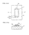
- Figs. 1(a) and 1(b) are explanatory views schematically showing an embodiment of the piezoelectric element of the present invention.
- Fig. 1(a) is a plan view
- Fig. 1(b) is a sectional view taken along the X-X' line of Fig. 1(a).
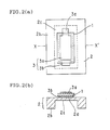
- Figs. 2(a) and 2(b) are explanatory views schematically showing another embodiment of the piezoelectric element of the present invention.
- Fig. 2(a) is a plan view
- Fig. 2(b) is a sectional view taken along the X-X' line of Fig. 2(a).
- Figs. 3(a) and 3(b) are explanatory views schematically showing still another embodiment of the piezoelectric element of the present invention.
- Fig. 3(a) is a plan view
- Fig. 3(b) is a sectional view taken along the X-X' line of Fig. 3(a).
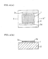
- Figs. 4(a) and 4(b) are explanatory views schematically showing still another embodiment of the piezoelectric element of the present invention.
- Fig. 4(a) is a plan view
- Fig. 4(b) is a sectional view taken along the X-X' line of Fig. 4(a).
- Figs. 5(a) and 5(b) are explanatory views schematically showing still another embodiment of the piezoelectric element of the present invention.
- Fig. 5(a) is a plan view
- Fig. 5(b) is a sectional view taken along the X-X' line of Fig. 5(a).
- Fig. 6 is a sectional view schematically showing still another embodiment of the piezoelectric element of the present invention.
- Fig. 7 is a sectional view schematically showing still another embodiment of the piezoelectric element of the present invention.
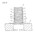
- Fig. 8 is a sectional view schematically showing still another embodiment of the piezoelectric element of the present invention.
- the piezoelectric element of the present invention is provided with: a ceramic substrate 2, a piezoelectric portion 1 composed of a specific piezoelectric ceramic composition, and electrodes 3 (3a and 3b).
- the electrodes 3 (3a and 3b) are electrically connected to the piezoelectric portion 1, and the piezoelectric portion 1 is solidly attached to the ceramic substrate 2 directly or via the electrodes 3.
- the present piezoelectric element is described specifically below at every constituent.
- the substrate 2 used in the present invention is of ceramics and preferably made of a material containing at least one kind selected from the group consisting of stabilized zirconium oxide, aluminum oxide, magnesium oxide, mullite, aluminum nitride, silicon nitride and glass, for the heat resistance, chemical stability and insulating property.
- a material containing stabilized zirconium oxide for the high mechanical strength and excellent tenacity.
- the substrate 2 has a thickness of preferably 3 ⁇ m to 1 mm, more preferably 5 to 500 ⁇ m, particularly preferably 7 to 200 ⁇ m in the present invention.
- the piezoelectric element When the thickness of the substrate 2 is less than 3 ⁇ m, the piezoelectric element may have a low mechanical strength; and when the thickness is more than 1 mm, the rigidity of the substrate relative to the shrinkage stress of the piezoelectric portion is large when a voltage is applied to the piezoelectric element, and the piezoelectric element may show a small flexural displacement.
- the substrate 2 may be produced so as to have, as shown in Figs. 2(a) and 2(b), a thin portion 2c roughly corresponding to an interface 2a between piezoelectric portion 1 or electrode 3b and ceramic substrate 2 and having the aforementioned thickness and a thick portion 2b roughly corresponding to the surface area of ceramic substrate other than the interface 2a and having a larger thickness than the thin portion 2c.
- the piezoelectric element obtained can show a larger flexural displacement and a higher mechanical strength.
- the surface shape of the substrate 2 in the present invention may be, for example, a rectangle, a square, a triangle, an ellipse, a true circle, an edge-rounded square, an edge-rounded rectangle, a capsule or a combination thereof.
- a cross-section of the substrate 2 in the thickness direction has a W-like shape having three inflection points in view of high linearity of a flexural displacement relative to an electric field.
- the piezoelectric portion 1 used in the present invention is a Pb(Mg, Ni) 1/3 Nb 2/3 O 3 -PbZrO 3 -PbTiO 3 ternary system solid solution composition and made of a piezoelectric ceramic composition represented by the following general formula (1).
- y in the above general formula (1) is preferably 0.08 - 0.18, and more preferably 0.10 - 0.15.
- Ni is preferably dispersed in the piezoelectric ceramic composition uniformly and more preferably in such a concentration gradient that the concentration of Ni becomes higher from the interface 2a between the piezoelectric portion and the substrate towards the thickness direction of the piezoelectric portion.
- the piezoelectric portion 1 can have a higher density even in the case that it is solidly attached to the substrate 2 directly or via an electrode.
- NiO in this piezoelectric ceramic composition is present as a particle having NiO as the main component.
- NiO particles enables to secure linearity of a flexural displacement relative to an electric field up to a high electric field region, and thereby a larger flexural displacement can be obtained in comparison with a conventional piezoelectric element with the same electric force.
- particles having NiO as the main component are preferably present on the surface and/or in the interior of the piezoelectric ceramic composition in the point that linearity of a flexural displacement relative to an electric field can be ensured up to a higher electric field region, more preferably unevenly distributed on the surface of the piezoelectric ceramic composition.
- unevenly distributed means “present in a part unevenly and includes both “present more on a surface than in the interior though they are present on the surface and in the interior of a piezoelectric ceramic composition” and “present only on the surface.”
- particles having NiO as the main component there is no particular limitation on a particle diameter of particles having NiO as the main component. However, it is preferably 0.1 - 2 ⁇ m.
- particles having NiO as the main component may be of only NiO or of MgO of solid solution. However, the particles of MgO of solid solution is preferable in view of high linearity of a flexural displacement.
- the Pb in the piezoelectric ceramic composition by at least one kind of element selected from the group consisting of Sr, Ca, Ba and La for improvement in piezoelectric properties and linearity of a flexural displacement relative to the amount of an electric field.
- the rate of replacement is preferably within a suitable range at every substituent element.
- the Pb in the piezoelectric ceramic composition is replaced by at least one kind of element selected from the group consisting of Sr, Ca and Ba
- the Pb is replaced preferably by 2 to 10 mole %, more preferably 4 to 8 mole %.
- the Pb in the piezoelectric ceramic composition is replaced by La
- the Pb is replaced preferably by 0.2 to 1.0 mole %, more preferably 0.4 to 0.9 mole %.
- a piezoelectric ceramic composition in the present invention preferably has an average particle diameter of 1 - 10 ⁇ m with a maximum particle diameter being 5 times as large as the average particle diameter or less, more preferably an average particle diameter of 2 - 5 ⁇ m with a maximum particle diameter being 4 times as large as the average particle diameter or less, furthermore preferably an average particle diameter of 2 - 5 ⁇ m with a maximum particle diameter being 3 times as large as the average particle diameter or less.
- the domain in the piezoelectric portion does not develop sufficiently, which is prone to cause deterioration in flexural displacement and linearity of a flexural displacement relative to an electric field in a high electric field region.
- the average particle diameter is more than 10 ⁇ m, the domain in the piezoelectric portion is large but does not move easily, which is prone to result in a small flexural displacement.
- the piezoelectric ceramic composition contains a phase other than perovskite phase preferably by 20% by volume or less, more preferably by 10% by volume or less.
- the piezoelectric ceramic composition has a porosity of preferably 10% by volume or less, more preferably 5% by volume or less for ensuring a desired flexural displacement and mechanical strength and enhancing linearity of a flexural displacement relative to an electric field in a high electric field region.
- the piezoelectric portion 1 in the present invention has a thickness of preferably 1 to 300 ⁇ m, more preferably 3 to 100 ⁇ m, particularly preferably 5 to 30 ⁇ m.
- the thickness of the piezoelectric portion 1 is less than 1 ⁇ m, even the piezoelectric portion made of the aforementioned specific piezoelectric ceramic composition is liable to be densified insufficiently.
- the thickness is more than 300 ⁇ m, the stress to the substrate becomes relatively too large; in order to prevent the substrate fracture, the ceramic substrate needs to have a larger thickness, making it difficult to produce a small piezoelectric element.
- the ratio of the thickness of the ceramic substrate 2 to the thickness of the piezoelectric portion 1 is preferably 0.1 to 30, more preferably 0.3 to 10, particularly preferably 0.5 to 5 from the point of ensuring mechanical strength and a desired flexural displacement.
- any electrode 3 may be employed as long as it is electrically connected to the piezoelectric portion 1.
- the electrodes 3 may be, for example, a pair of comb-shaped electrodes 3c and 3d formed on a piezoelectric portion 1 attached solidly to a substrate 2 as shown in Figs. 4(a) and 4(b); or, may be a pair of comb-shaped electrodes 3c and 3d attached solidly to a substrate 2 with a piezoelectric portion 1 being solidly attached onto the electrodes 3c and 3d as shown in Fig. 5(a) and 5(b).
- a piezoelectric portion 1 is solidly attached, and a common electrode 3e is formed on a surface opposite to the surface of the piezoelectric portion 1 where the comb-shaped electrodes 3c and 3d are solidly attached.
- a piezoelectric portion 1 is solidly attached, and a pair of comb-shaped electrodes 3c and 3d are formed on a surface opposite to the surface of the piezoelectric portion 1 where the common electrode 3e is solidly attached.
- a layered piezoelectric element where a plurality of piezoelectric portions (1a - 1k) are arranged in stories as shown in Fig. 8, preferably has a negative electrode 3f and a positive electrode 3g of the electrode 3 are alternatively interposed between the electrode portions (1a - 1k).
- a width of an electrode is preferably 60 - 90% of a width of a piezoelectric portion, and more preferably 70 - 80%.
- a flexural displacement becomes small because an area of the piezoelectric portion where an electric field is applied is small.
- a width of an electrode is more than 90% of a width of a piezoelectric portion, positioning of the electrode requires precision, and bad precision upon positioning causes a short between electrodes or dielectric breakdown.
- the material for the electrodes 3 there is no limitation and may be employed, for example, a material made of at least one kind selected from the group consisting of platinum, palladium, rhodium, gold, silver and alloys thereof. A glass component may be added thereto further upon the heat treatment described below to make formation of an electrode easy. Of these materials, platinum or an alloy composed mainly of platinum is preferred because they show high heat resistance during the heat-treatment of piezoelectric portion. In the case of the aforementioned layered piezoelectric element, a material for each electrode may be the same among all electrodes or different in a part of or all the electrodes.
- the thickness of electrodes 3 in the present invention is preferably 15 ⁇ m or less, more preferably 5 ⁇ m or less because, when the thickness is more than 15 ⁇ m, the electrodes 3 act as a relaxing layer, which may result in a small flexural displacement.
- each of the aforementioned elements for constituting the piezoelectric element is in a specific state, that is, the piezoelectric portion 1 is solidly attached to the substrate 2 directly or via the aforementioned electrode.
- be solidly attached refers to that the piezoelectric portion is tightly integrated with the ceramic substrate directly or via the electrode, owing to a solid-state reaction between the ceramic substrate and the piezoelectric portion or the electrode, without using any organic or inorganic adhesive.
- the piezoelectric portion 1a at the lowest portion is solidly attached to the substrate 2 directly or via the electrode 3g.
- the ratio of the capacity after polarization to the capacity before polarization is preferably 120% or more, more preferably 125% or more, in the point of an easily movable polarization structure.
- a piezoelectric material made of a specific piezoelectric ceramic composition is superposed on a ceramic substrate or an electrode formed on a ceramic substrate.
- the substrate used in the present invention can be produced by producing a compact having a desired shape by a general method of, for example, a press and an extrusion with using a material corresponding with the ceramics as described with respect to the piezoelectric element of the present invention and firing the compact under general firing conditions.
- the piezoelectric material used in the present invention is made of a piezoelectric ceramic composition described with respect to the piezoelectric element of the present invention and can be prepared as follows.
- a mixture is prepared by mixing simple substances (elements) each consisting of Pb, Ba, Ca, Sr, La, Mg, Ni, Nb, Zr or Ti; oxides of these elements (e.g. PbO, Pb 3 O 4 , La 2 O 3 , MgO, NiO, Nb 2 O 5 , TiO 2 and ZrO 2 ); carbonates of these elements (e.g. BaCO 3 , SrCO 3 , MgCO 3 and CaCO 3 ); and compounds containing a plurality of these elements (e.g.
- the mixture has an average particle diameter of preferably 1 ⁇ m or less, more preferably 0.5 ⁇ m or less in the point that they can easily be uniformly mixed.
- the resulting mixed raw material is calcined at 750 to 1,300°C to obtain a piezoelectric ceramic composition.
- the calcined piezoelectric ceramic composition has a ratio of a strength of the strongest diffraction ray of a perovskite phase to a strength of the strongest diffraction ray of a pyrochlore phase is preferably 5% or less, more preferably 2% or less.
- the piezoelectric ceramic composition obtained above is ground with a grinding apparatus such as a ball mill, an attrition mill, or a beads mill to give a piezoelectric material powder having a desired particle diameter.
- a grinding apparatus such as a ball mill, an attrition mill, or a beads mill to give a piezoelectric material powder having a desired particle diameter.
- the average particle diameter of the piezoelectric material powder is preferably 0.1 - 1.0 ⁇ m, more preferably 0.3 - 0.7 ⁇ m.
- the maximum particle diameter of the piezoelectric material powder is preferably 3.0 ⁇ m or less, and more preferably 2.0 ⁇ m or less.
- a particle diameter of the powder may be adjusted by subjecting the piezoelectric material powder obtained by grinding to a heat treatment at 400 - 750°C. At this time, a finer particle is more preferable because a fine particle can be integrated with other particles to give a powder having an even particle diameter.
- the piezoelectric material may be prepared by another method, for example, an alkoxide method or a co-precipitation method.
- the method for superposing the obtained piezoelectric material may be, for example, screen printing, spraying or dipping. Of these, screen printing is preferred because it enables continuous lamination easily in a shape and thickness of high accuracy.
- a piezoelectric material is superposed directly on a substrate.
- an electrode is formed on a substrate, and a piezoelectric material is superposed on the electrode.
- the method for coating the piezoelectric material there can be mentioned, for example, an ion beam method, sputtering, vacuum deposition, PVD, ion plating, CVD, plating, screen printing, spraying and dipping.
- sputtering and screen printing are preferred in view of the bondability between a ceramic substrate and a piezoelectric portion.
- the formed electrode can be integrated with a substrate and/or a piezoelectric portion by a heat treatment of at about 1000 - 1400°C.
- the heat treatment may be conducted before a piezoelectric material is superposed, at the time when an electrode is formed, or collectively by a heat treatment conducted after a piezoelectric material is superposed as described below.
- the piezoelectric material superposed on the ceramic substrate or on the electrode is heat-treated in the co-presence of an atmosphere-controlling material having the same composition as the piezoelectric composition in a sealing atmosphere.
- the atmosphere-controlling material is made to coexist at preferably 0.03 - 0.50 mg/cm 3 , more preferably 0.07 - 0.40 mg/cm 3 , furthermore preferably 0.10 - 0.30 mg/cm 3 in terms of NiO amount per unit volume of a space in a container in the atmosphere.
- NiO can be dispersed uniformly in a piezoelectric portion by making a NiO content of a co-existing atmosphere-controlling material the same as an piezoelectric ceramic composition constituting a piezoelectric material, and NiO can be dispersed in such a concentration gradient that the concentration of NiO becomes higher from the interface between the piezoelectric portion and the ceramic substrate towards the thickness direction of the piezoelectric portion by giving a higher concentration to a piezoelectric ceramic composition constituting a piezoelectric material.
- NiO content of the composition made to be co-exist it becomes possible to control the extent of the NiO concentration gradient in the piezoelectric obtained.
- a container for housing the piezoelectric element and a setter for mounting the piezoelectric element thereon a member obtained by subjecting the member to a heat treatment (hereinbelow sometimes referred to simply as "pretreatment") in an atmosphere where an atmosphere-controlling material having the same composition as the piezoelectric material is coexisted.
- pretreatment a heat treatment
- a piezoelectric material it is particularly preferable to subject a piezoelectric material to a heat treatment with using the pretreated container and setter as well as to make a specific amount of the aforementioned atmosphere-controlling material co-exist.
- Such a heat treatment gives a piezoelectric portion where a ceramic composition contains particles having NiO on the surface and in the interior thereof, and a piezoelectric element having a higher linearity of a flexural displacement relative to an electric field up to a high electric field region.
- a material for the container and the setter in the present invention contains, as the main component, magnesium oxide, aluminum oxide, zirconium oxide, mullite, or spinel.
- the pretreatment is preferably conducted at a temperature within a range of ⁇ 100°C from a temperature for heat treating a material for a piezoelectric portion superposed on a substrate or the like so that an effect due to the pretreatment is sufficiently exhibited.
- the pretreatment is conducted preferably plural times, more preferably at least 3 times to make securely present particles having NiO as the main component on the surface and in the interior of the ceramic composition.
- the heat treatment temperature for the piezoelectric material is preferably 1,000 to 1,400°C, more preferably 1,100 to 1,350°C.
- the temperature is less than 1,000°C, the solid attachment of the piezoelectric to the ceramic substrate may be insufficient or the density of the piezoelectric may be insufficient.
- the temperature exceeds 1,400°C, the vaporization amount of Pb and Ni in the piezoelectric material is large and it may be difficult to obtain a piezoelectric having an intended composition.
- the time for keeping the highest temperature of the heat treatment is preferably 10 min. - 10 hours, more preferably 1 hour - 4 hours.
- each electrode and each piezoelectric portion may be heat-treated by every formation thereof, may be heat-treated after all of them are formed, or may be heat-treated repeatedly after some of them are formed.
- the ratio of the capacity after polarization to the capacity before polarization is preferably 120% or more, more preferably 125% or more, in the point of an easily movable polarization structure.
- a voltage was applied to electrodes of a piezoelectric element so as to give an electric field of 3 kV/mm.
- the resulting flexural displacement of the piezoelectric element was measured by a laser displacement tester.
- a surface of a ternary system solid solution composition constituting a piezoelectric portion was measured with a scanning electron microscope.
- a line was drawn on an optional image for observation, a distance of a grain boundary across the line was defined as a particle diameter, particle diameters of 100 ternary system solid solution compositions were measured to determine the average particle diameter and the maximum particle diameter.
- the piezoelectric portion of each piezoelectric element obtained in Examples and Comparative Examples was examined by a scanning electron microscope, over a range of 50 ⁇ m of each of the surface, length and width; the areal proportion of pores in each of the three visual fields was determined; and the average of the three areal proportions was calculated and taken as the porosity of the piezoelectric portion.
- Evaluation was made with a ratio of a flexural displacement after continuous application of a voltage to give an electric field of 4kV/mm with a frequency of 1kHz continuously 1x 10 8 times between electrodes to a flexural displacement before the continuous application. That is, durability is 100% when a flexural displacement is not changed after the continuous application, and durability is 0% when a flexural displacement becomes 0 after the continuous application.
- a rate of the number of piezoelectric elements having dielectric breakdown relative to the number of whole piezoelectric elements was evaluated as a rate of dielectric breakdown in the case that a voltage was applied between electrodes so as to give an electric field of 4 kV/mm.
- a lower electrode [1.2 mm x 0.8 mm x 3 ⁇ m (thickness)] composed of platinum was formed, by screen printing, on a Y 2 O 3 -stabilized ZrO 2 substrate [dimensions of the thin portion: 1.6 mm x 1.1 mm x 10 ⁇ m (thickness) with a shape of cross-section in a longitudinal direction being rectangle (a surface where a piezoelectric portion or an electrode is flat)]. They were subjected to a heat treatment at 1300°C for two hours to integrate the lower electrode with the substrate.
- a piezoelectric material [1.3 mm x 0.9 mm x 13 ⁇ m (thickness)] made of Pb 1.00 ⁇ (Mg 0.87 Ni 0.13 ) 1/3 Nb 2/3 ⁇ 0.20 Ti 0.43 Zr 0.37 O 3 having the average particle diameter of 0.45 ⁇ m and the maximum particle diameter of 1.8 ⁇ m.
- the substrate having a piezoelectric material superposed thereon was subjected to a heat-treatment at 1,275°C for 2 hours in the co-presence of an atmosphere-controlling material having the same composition as the piezoelectric material at the rate of 0.15 mg/cm 3 in terms of NiO per unit volume of the space in the container.
- the piezoelectric material after the heat treatment had a thickness of 10 ⁇ m.
- a container and a setter to be used was heat-treated (hereinbelow sometimes referred to as "pretreatment") once in the co-presence of an atmosphere-controlling material having the same composition as the piezoelectric material at the rate of 0.15 mg/cm 3 in terms of NiO per unit volume of the space in the container to be adapted to the atmosphere. Housing in the container and mounting on the setter were performed.
- an upper electrode [1.2 mm x 0.8 mm x 0.5 ⁇ m (thickness)] composed of gold.
- the resulting material was heat-treated to produce a piezoelectric element.
- a piezoelectric element was produced in the same manner as in Example 1 except that there was used a a piezoelectric material made of Pb 1.00 ⁇ (Mg 0.87 Ni 0.13 ) 1/3 Nb 2/3 ⁇ 0.20 Ti 0.43 Zr 0.37 O 3 having the average particle diameter of 0.51 ⁇ m and the maximum particle diameter of 5.3 ⁇ m.
- a piezoelectric element of Example 1 had an average particle diameter of 2.2 ⁇ m, the maximum particle diameter of 5.9 ⁇ m, the ratio of the 4kV/mm flexural displacement to the 2kV/mm flexural displacement (hereinbelow sometimes referred to as "4/2 flexural displacement ratio) was 165%, which shows high linearity of a flexural displacement relative to an electric field.
- the flexural displacement itself was so large as 2.18 ⁇ m.
- the maximum particle diameter was 15.5 ⁇ m, which is above 5 times the average particle diameter, though the particle diameter was 2.3 ⁇ m.
- This piezoelectric element had a 4/2 flexural displacement ratio of 151%, which shows lower linearity of a flexural displacement relative to an electric field than a piezoelectric element in Example 1.
- the flexural displacement itself was 1.81 ⁇ m, which is smaller than that of a piezoelectric element in Example 1.
- the results are collectively shown in Table 1. Average particle diameter ( ⁇ m) Maximum particle diameter ( ⁇ m) Maximum particle diameter/ Average particle diameter 4/2 flexural displacement ratio (%) Flexural displacement ( ⁇ m) Example 1 2.2 5.9 2.7 165 2.18 Comp. Ex. 1 2.3 15.5 6.7 151 1.81
- Piezoelectric elements were produced in the same manner as in Example 1 except that there were used, as piezoelectric materials, those obtained by mixing 97% by volume, 93% by volume or 85% by volume of a piezoelectric ceramic composition made of Pb 1.00 ⁇ (Mg 0.87 Ni 0.13 ) 1/3 Nb 2/3 ⁇ 0.20 Ti 0.43 Zr 0.37 O 3 , with 3% by volume, 7% by volume or 15% by volume of a latex having particle diameters of 8 to 12 ⁇ m.
- a piezoelectric element of Reference Example 3 (15% by volume of a latex is mixed in a piezoelectric material) had a porosity of 19%. At that time, the 4/2 flexural displacement ratio was 139%, and a flexural displacement itself was 1.65 ⁇ m.
- a piezoelectric element of Reference Example 2 (7% by volume of a latex is mixed in a piezoelectric material) had a porosity of 10%. At that time, the 4/2 flexural displacement ratio was 151%, and a flexural displacement itself was 1.93 ⁇ m.
- a piezoelectric element of Reference Example 1 (3% by volume of a latex is mixed in a piezoelectric material) had a porosity of 5%.
- a piezoelectric element was produced in the same manner as in Example 1 except that a piezoelectric element made of a ternary system solid solution composition having a different Ni ratio (y) as shown in Table 3.
- a piezoelectric element in Example 1 which had a Ni ratio (y) of 0.13 in a composition, had a small porosity (3%),and a ratio of a flexural displacement after continuous application to a flexural displacement before continuous application was 94%, showing very excellent durability. In addition, a flexural displacement was large (2.18 ⁇ m).
- a piezoelectric element of Comparative Example 1 with a low ratio (0.03) of Ni (y) in the composition had a large porosity (13%), and a ratio of a flexural displacement after continuous application to a flexural displacement before continuous application was 89%, showing a durability inferior to a piezoelectric element of Example 1.
- a flexural displacement was 1.96 ⁇ m, which is smaller than that of a piezoelectric element of Examples.
- a piezoelectric element was produced in the same manner as in Example 1 except that a piezoelectric material made of Pb 1.00 ⁇ (Mg 0.84 Ni 0.16 ) 0.97/3 Nb 2/3 ⁇ 0.20 Ti 0.43 Zr 0.37 O 3 was laminated.
- a piezoelectric element was produced in the same manner as in Example 1 except that a piezoelectric material made of Pb 1.00 ⁇ (Mg 0.80 Ni 0.20 ) 0.97/3 Nb 2/3 ⁇ 0.20 Ti 0.43 Zr 0.37 O 3 was laminated on a piezoelectric material made of Pb 1.00 ⁇ (Mg 0.95 Ni 0.05 ) 0.97/3 Nb 2/3 ⁇ 0.20 Ti 0.43 Zr 0.37 O 3 laminated on an electrode unitarily joined with a ZrO 2 substrate.
- a piezoelectric element was produced in the same manner as in Example 1 except that a piezoelectric material made of Pb 1.00 ⁇ (Mg 0.80 Ni 0.20 ) 0.97/3 Nb 2/3 ⁇ 0.20 Ti 0.43 Zr 0.37 O 3 was laminated on a piezoelectric material made of Pb 1.00 ⁇ (Mg 0.95 Ni 0.05 ) 0.97/3 Nb 2/3 ⁇ 0.20 Ti 0.43 Zr 0.37 O 3 laminated on an electrode unitarily joined with a ZrO 2 substrate and a container and a setter both subjected to a pretreatment three times upon a heat treatment.
- a piezoelectric element in Example 3 had a 4/2 flexural displacement ratio of 168%, showing a relatively high linearity of a flexural displacement relative to an electric field, and a flexural displacement was large (2.22 ⁇ m).
- the dispersion state of NiO in a piezoelectric portion was examined by an EPMA analysis, and no particle having NiO as the main component was not observed.
- a piezoelectric element of Example 4 had a 4/2 flexural displacement ratio of 172%, showing higher linearity of a flexural displacement relative to electric fields than that of a piezoelectric element of Example 3, and a flexural displacement was about the same.
- the dispersion state of NiO in a piezoelectric portion was examined by an EPMA analysis, which indicated that particles having NiO as the main component were not present in the interior of the piezoelectric portion though they were present on a surface of the piezoelectric portion. Further, it was found that Ni was dispersed in the piezoelectric ceramic composition in such a concentration gradient that the concentration of Ni becomes higher from the interface between the piezoelectric portion and the substrate towards the thickness direction of the piezoelectric portion.
- a piezoelectric element of Example 5 had a 4/2 flexural displacement ratio of 177%, showing the highest linearity of a flexural displacement relative to an electric field, and a flexural displacement was about the same.
- the dispersion state of NiO in a piezoelectric portion was examined by an EPMA analysis, which indicated that particles having NiO as the main component were present both on a surface and in the interior of the piezoelectric portion.
- Mg was detected. The results are collectively shown in Table 4.
- a piezoelectric element was produced in the same manner as in Example 1 except that a piezoelectric material having a composition shown in Table 5 was used.
- a piezoelectric element of Example 6, where a total ratio of Mg and Ni in a piezoelectric material is within the range (a 0.97), had a 4/2 flexural displacement ratio of 170%, showing high linearity of a flexural displacement relative to an electric field, and a flexural displacement itself was large (2.25 ⁇ m).
- a piezoelectric element was produced in the same manner as in Example 1 except that a piezoelectric material having a composition shown in Table 6 was used.
- the results are collectively shown in Table 6.
- a piezoelectric element was produced in the same manner as in Example 1 except that a piezoelectric material having a composition shown in Table 7 was used.
- any of the piezoelectric elements in Examples 8 - 11 had a 4/2 flexural displacement ratio of 160% or more, showing relatively high linearity of flexural displacement relative to an electric field, and a flexural displacement was large (2.19 ⁇ m or more).
- a piezoelectric element of Example 9 employing a piezoelectric material having a composition where 5.0 mol% of Pb was substituted by Sr and a piezoelectric element of Example 10 employing a piezoelectric material having a composition where10.0 mol% of Pb was substituted by Ba had a 4/2 flexural displacement ratio of 169% and 166%, respectively, showing higher linearity of a flexural displacement relative to an electric field in comparison with a piezoelectric element of Example 8 employing a piezoelectric material having a composition where Pb is not substituted at all.
- a piezoelectric element of Example 11 employing a piezoelectric material where 7.5 mol% of Pb was substituted by Sr, and other 7.5 mol% of Pb was substituted by Ca (15 mol% in total) had a 4/2 flexural displacement ratio of 160%, showing lower linearity of a flexural displacement relative to an electric field in comparison with a piezoelectric element of Example 8 employing a piezoelectric material having a composition where Pb is not substituted at all.
- a piezoelectric element was produced in the same manner as in Example 1 except that a piezoelectric material having a composition shown in Table 8 was used.
- any of the piezoelectric elements in Examples 12 and 13 had a 4/2 flexural displacement ratio of 161% or more, showing relatively high linearity of a flexural displacement relative to an electric field.
- a piezoelectric element of Example 12 employing a piezoelectric material where 0.8 mol% of Pb is substituted by La had a 4/2 flexural displacement ratio of 167%, showing higher linearity of a flexural displacement relative to an electric field in comparison with that of a piezoelectric element of Example 8 employing a piezoelectric material where a part of Pb was not substituted by La.
- the flexural displacement itself was larger (2.30 ⁇ m).
- a piezoelectric element of Example 13 employing a piezoelectric material where 1.5 mol% of Pb is substituted by La had a 4/2 flexural displacement ratio of 161%, showing lower linearity of a flexural displacement relative to an electric field in comparison with that of a piezoelectric element of Example 8.
- the flexural displacement itself was small (2.18 ⁇ m) in comparison with that of the piezoelectric element in Example 11. The results are shown in Table 8.
- a piezoelectric element was produced in the same manner as in Example 1 except that a piezoelectric material made of Pb 1.00 ⁇ (Mg 0.90 Ni 0.10 ) 1/3 Nb 2/3 ⁇ 0.20 Ti 0.43 Zr 0.37 O 3 was laminated, that a heat treatment was conducted in the co-presence of an atmosphere-controlling material at 0.15 mg/cm 3 , 0.750 mg/cm 3 , 0.015 mg/cm 3 , respectively, in terms of NiO amount per unit volume of a space in a container, and that a container and a setter without being subjected to a pretreatment were used.
- Example 4 where the heat treatment was conducted in the co-presence of 0.15mg/cm 3 of an atmosphere-controlling material in terms of a NiO amount per unit volume of a space in a container, the 4/2 flexural displacement ratio was 167%, showing high linearity of a flexural displacement.
- the results are collectively shown in Table 9. Atmosphere-controlling material ... NiO conversion amount per unit volume (mg/cm 3 ) Dielectric breakdown ratio (%) 4/2 flexural displacement ratio (%) Flexural displacement ( ⁇ m)
- Example 14 0.150 2 167 2.29 Comp. Ex. 6 0.750 15 164 2.01 Comp. Ex. 7 0.015 2 144 1.58
- a piezoelectric element was produced in the same manner as in Example 1 except that a substrate having a W-like sectional shape in a thickness direction was used and that a piezoelectric material made of Pb 1.00 ⁇ (Mg 0.90 Ni 0.10 ) 1/3 Nb 2/3 ⁇ 0.20 Ti 0.43 Zr 0.37 O 3 was used.
- a piezoelectric element was produced in the same manner as in Example 1 except that a piezoelectric material made of Pb 1.00 ⁇ (Mg 0.90 Ni 0.10 ) 1/3 Nb 2/3 ⁇ 0.20 Ti 0.43 Zr 0.37 O 3 was used.
- a sectional shape of a substrate in a thickness direction was rectangular (having a flat plane where a piezoelectric portion and an electrode are solidly attached) as in Example 1.
- a flexural displacement itself was larger (2.49 ⁇ m) in comparison with a piezoelectric element of Example 16.
- a piezoelectric element was produced in the same manner as in Example 1 except that there was used a layered piezoelectric element having a negative electrode, a piezoelectric material, a positive electrode, a piezoelectric material and negative electrode superposed on a substrate in this order, and having a negative electrode and a positive electrode alternatively interposed between two piezoelectric portions with the bottom piezoelectric portion being solidly adhered to the substrate via an electrode, and that a thickness of layered material was made half of that of Example 1 to make a thickness of each piezoelectric portion to be 5 ⁇ m (10 ⁇ m as a whole as in Example 1).
- a piezoelectric element of Example 1 having only one layer in the piezoelectric portion had a large 4/2 flexural displacement ratio of 165%, showing high linearity of a flexural potential relative to an electric field.
- a piezoelectric element of Example 17 having each piezoelectric portion having a half thickness and two layers had a 4/2 flexural displacement ratio of 161%, showing lower linearity of a flexural potential to an electric field that a piezoelectric element of Example 1.
- a flexural displacement itself was larger (2.30 ⁇ m) than a piezoelectric element of Example 1. The results are collectively shown in Table 11. Thickness of piezoelectric portion ( ⁇ m) Number of layers in piezoelectric portion 4/2 flexural displacement ratio (%) Flexural displacement ( ⁇ m) Example 1 10 1 165 2.18 Example 17 5 2 161 2.30
- a piezoelectric element which has very high piezoelectric properties, excellent vibration transmittability between a ceramic substrate and a piezoelectric portion, high linearity of a flexural displacement relative to an electric field, and a high durability even in the use for a long period of time with a large flexural displacement, and a method for production thereof.
- the piezoelectric element of the present invention can be suitably used for an actuator, a sensor, etc.
Landscapes
- Engineering & Computer Science (AREA)
- Chemical & Material Sciences (AREA)
- Manufacturing & Machinery (AREA)
- Inorganic Chemistry (AREA)
- Ceramic Engineering (AREA)
- Compositions Of Oxide Ceramics (AREA)
Applications Claiming Priority (2)
| Application Number | Priority Date | Filing Date | Title |
|---|---|---|---|
| JP2001388315A JP3953806B2 (ja) | 2001-12-20 | 2001-12-20 | 圧電素子、及びその製造方法 |
| JP2001388315 | 2001-12-20 |
Publications (3)
| Publication Number | Publication Date |
|---|---|
| EP1321987A2 true EP1321987A2 (de) | 2003-06-25 |
| EP1321987A3 EP1321987A3 (de) | 2004-12-01 |
| EP1321987B1 EP1321987B1 (de) | 2008-10-22 |
Family
ID=19188136
Family Applications (1)
| Application Number | Title | Priority Date | Filing Date |
|---|---|---|---|
| EP20020258796 Expired - Lifetime EP1321987B1 (de) | 2001-12-20 | 2002-12-19 | Piezoelektrisches Bauelement und Verfahren zu dessen Herstellung |
Country Status (3)
| Country | Link |
|---|---|
| EP (1) | EP1321987B1 (de) |
| JP (1) | JP3953806B2 (de) |
| DE (1) | DE60229488D1 (de) |
Cited By (7)
| Publication number | Priority date | Publication date | Assignee | Title |
|---|---|---|---|---|
| US6888292B2 (en) | 2002-02-08 | 2005-05-03 | Ngk Insulators, Ltd. | Multi-layered type piezoelectric device and process for production thereof |
| EP1471584A3 (de) * | 2003-03-31 | 2006-03-22 | Ngk Insulators, Ltd. | Piezoelektrisches/elektrostriktives Filmbauelement und piezoelektrische/elektrostriktive Keramik-Zusammensetzung |
| EP1575100A3 (de) * | 2004-03-03 | 2006-08-23 | Ngk Insulators, Ltd. | Piezoelektrische/elektrostriktive keramische Zusammensetzung und piezoelektrisches/elektrostriktives Dünnschichtbauteil |
| US7161284B2 (en) | 2003-05-21 | 2007-01-09 | Ngk Insulators, Ltd. | Multilayered piezoelectric/electrostrictive device |
| EP1684364A3 (de) * | 2005-01-20 | 2007-03-21 | Ngk Insulators, Ltd. | Piezoelektrisches Bauteil |
| US8742650B2 (en) | 2007-02-20 | 2014-06-03 | Ngk Insulators, Ltd. | Piezoelectric/electrostrictive element |
| CN119350021A (zh) * | 2024-10-22 | 2025-01-24 | 浙江嘉康电子股份有限公司 | 具有高压电常数的金属化合物掺杂pzt基压电陶瓷材料及其超低温烧结制备方法 |
Families Citing this family (9)
| Publication number | Priority date | Publication date | Assignee | Title |
|---|---|---|---|---|
| JP2004136461A (ja) | 2002-10-15 | 2004-05-13 | Brother Ind Ltd | 液体圧力発生機構 |
| JP2005170693A (ja) | 2003-12-08 | 2005-06-30 | Ngk Insulators Ltd | 圧電/電歪磁器組成物、圧電/電歪体、及び圧電/電歪膜型素子 |
| JP2005183701A (ja) * | 2003-12-19 | 2005-07-07 | Murata Mfg Co Ltd | 圧電素子及びその製造方法 |
| JP4537212B2 (ja) | 2005-01-11 | 2010-09-01 | 日本碍子株式会社 | 圧電/電歪素子の製造方法 |
| JP5004484B2 (ja) | 2006-03-23 | 2012-08-22 | 日本碍子株式会社 | 誘電体デバイス |
| US7727584B2 (en) | 2007-02-19 | 2010-06-01 | Ngk Insulators, Ltd. | Dielectric device and its manufacturing method |
| US7727585B2 (en) | 2007-02-19 | 2010-06-01 | Ngk Insulators, Ltd. | Dielectric device and its manufacturing method |
| JP4538493B2 (ja) | 2007-12-18 | 2010-09-08 | 日本碍子株式会社 | 圧電/電歪膜型素子 |
| JP5054149B2 (ja) * | 2010-04-26 | 2012-10-24 | 日本碍子株式会社 | 圧電/電歪膜型素子 |
Family Cites Families (7)
| Publication number | Priority date | Publication date | Assignee | Title |
|---|---|---|---|---|
| JPS503519B1 (de) * | 1970-11-11 | 1975-02-05 | ||
| JPS60102779A (ja) * | 1983-11-09 | 1985-06-06 | Hitachi Metals Ltd | 圧電磁器組成物 |
| MY104019A (en) * | 1988-05-27 | 1993-10-30 | Mitsui Chemicals Inc | Ferroelectric ceramic material. |
| US5275988A (en) * | 1991-04-12 | 1994-01-04 | Nec Corporation | Ceramic composition |
| JP3151644B2 (ja) * | 1993-03-08 | 2001-04-03 | 日本碍子株式会社 | 圧電/電歪膜型素子 |
| US5900274A (en) * | 1998-05-01 | 1999-05-04 | Eastman Kodak Company | Controlled composition and crystallographic changes in forming functionally gradient piezoelectric transducers |
| AU2001267477A1 (en) * | 2000-05-26 | 2001-12-11 | Ceramtec Ag | Internal electrode material for piezoceramic multilayer actuators |
-
2001
- 2001-12-20 JP JP2001388315A patent/JP3953806B2/ja not_active Expired - Fee Related
-
2002
- 2002-12-19 DE DE60229488T patent/DE60229488D1/de not_active Expired - Lifetime
- 2002-12-19 EP EP20020258796 patent/EP1321987B1/de not_active Expired - Lifetime
Cited By (10)
| Publication number | Priority date | Publication date | Assignee | Title |
|---|---|---|---|---|
| US6888292B2 (en) | 2002-02-08 | 2005-05-03 | Ngk Insulators, Ltd. | Multi-layered type piezoelectric device and process for production thereof |
| US7484278B2 (en) | 2002-02-08 | 2009-02-03 | Ngk Insulators, Ltd. | Method of manufacturing a multi-layered piezoelectric |
| EP1471584A3 (de) * | 2003-03-31 | 2006-03-22 | Ngk Insulators, Ltd. | Piezoelektrisches/elektrostriktives Filmbauelement und piezoelektrische/elektrostriktive Keramik-Zusammensetzung |
| US7161284B2 (en) | 2003-05-21 | 2007-01-09 | Ngk Insulators, Ltd. | Multilayered piezoelectric/electrostrictive device |
| EP1575100A3 (de) * | 2004-03-03 | 2006-08-23 | Ngk Insulators, Ltd. | Piezoelektrische/elektrostriktive keramische Zusammensetzung und piezoelektrisches/elektrostriktives Dünnschichtbauteil |
| US7309949B2 (en) | 2004-03-03 | 2007-12-18 | Ngk Insulators, Ltd. | Piezoelectric/electrostrictive porcelain composition, piezoelectric/electrostrictive ceramic and piezoelectric/electrostrictive film type device |
| EP1684364A3 (de) * | 2005-01-20 | 2007-03-21 | Ngk Insulators, Ltd. | Piezoelektrisches Bauteil |
| US8742650B2 (en) | 2007-02-20 | 2014-06-03 | Ngk Insulators, Ltd. | Piezoelectric/electrostrictive element |
| US9178130B2 (en) | 2007-02-20 | 2015-11-03 | Ngk Insulators, Ltd. | Piezoelectric/electrostrictive element |
| CN119350021A (zh) * | 2024-10-22 | 2025-01-24 | 浙江嘉康电子股份有限公司 | 具有高压电常数的金属化合物掺杂pzt基压电陶瓷材料及其超低温烧结制备方法 |
Also Published As
| Publication number | Publication date |
|---|---|
| EP1321987B1 (de) | 2008-10-22 |
| EP1321987A3 (de) | 2004-12-01 |
| DE60229488D1 (de) | 2008-12-04 |
| JP3953806B2 (ja) | 2007-08-08 |
| JP2002217465A (ja) | 2002-08-02 |
Similar Documents
| Publication | Publication Date | Title |
|---|---|---|
| US6610427B2 (en) | Piezoelectric element and process for production thereof | |
| US6565997B2 (en) | Piezoelectric element and process for production thereof | |
| EP1321987B1 (de) | Piezoelektrisches Bauelement und Verfahren zu dessen Herstellung | |
| US6888292B2 (en) | Multi-layered type piezoelectric device and process for production thereof | |
| US7052732B2 (en) | Method for producing a piezoelectric element | |
| EP1321986B1 (de) | Piezoelektrisches Bauelement und Verfahren zu dessen Herstellung | |
| EP1684364A2 (de) | Piezoelektrisches Bauteil | |
| US7545084B2 (en) | Piezoelectric/electrostrictive ceramic composition, piezoelectric/electrostrictive device, and method of producing the same | |
| US7176155B2 (en) | Piezoelectric/electrostrictive ceramic composition, piezoelectric/electrosrictive material, and piezoelectric/electrostrictive film device | |
| EP1471584B1 (de) | Piezoelektrisches/elektrostriktives Filmbauelement und piezoelektrische/elektrostriktive Keramikzusammensetzung | |
| JP4777605B2 (ja) | 多層型圧電/電歪素子 | |
| JP2005247619A (ja) | 圧電/電歪磁器組成物、圧電/電歪体、及び圧電/電歪膜型素子 | |
| EP0926746A2 (de) | Piezoelektrisches Antriebelement und damit ausgestatteter Tintenstrahldruckkopf | |
| US20060290240A1 (en) | Piezoelectric/electrostrictive porcelain composition, piezoelectric/electrostrictive body, and piezoelectric/electrostrictive film type device | |
| JP2006100853A (ja) | 圧電素子、及びその製造方法 | |
| JP2004153252A (ja) | 圧電体素子、及びその製造方法 |
Legal Events
| Date | Code | Title | Description |
|---|---|---|---|
| PUAI | Public reference made under article 153(3) epc to a published international application that has entered the european phase |
Free format text: ORIGINAL CODE: 0009012 |
|
| AK | Designated contracting states |
Designated state(s): AT BE BG CH CY CZ DE DK EE ES FI FR GB GR IE IT LI LU MC NL PT SE SI SK TR |
|
| AX | Request for extension of the european patent |
Extension state: AL LT LV MK RO |
|
| PUAL | Search report despatched |
Free format text: ORIGINAL CODE: 0009013 |
|
| AK | Designated contracting states |
Kind code of ref document: A3 Designated state(s): AT BE BG CH CY CZ DE DK EE ES FI FR GB GR IE IT LI LU MC NL PT SE SI SK TR |
|
| AX | Request for extension of the european patent |
Extension state: AL LT LV MK RO |
|
| 17P | Request for examination filed |
Effective date: 20050214 |
|
| 17Q | First examination report despatched |
Effective date: 20050408 |
|
| AKX | Designation fees paid |
Designated state(s): DE FR GB |
|
| GRAP | Despatch of communication of intention to grant a patent |
Free format text: ORIGINAL CODE: EPIDOSNIGR1 |
|
| GRAS | Grant fee paid |
Free format text: ORIGINAL CODE: EPIDOSNIGR3 |
|
| GRAA | (expected) grant |
Free format text: ORIGINAL CODE: 0009210 |
|
| AK | Designated contracting states |
Kind code of ref document: B1 Designated state(s): DE FR GB |
|
| REG | Reference to a national code |
Ref country code: GB Ref legal event code: FG4D |
|
| REF | Corresponds to: |
Ref document number: 60229488 Country of ref document: DE Date of ref document: 20081204 Kind code of ref document: P |
|
| PLBE | No opposition filed within time limit |
Free format text: ORIGINAL CODE: 0009261 |
|
| STAA | Information on the status of an ep patent application or granted ep patent |
Free format text: STATUS: NO OPPOSITION FILED WITHIN TIME LIMIT |
|
| 26N | No opposition filed |
Effective date: 20090723 |
|
| PGFP | Annual fee paid to national office [announced via postgrant information from national office to epo] |
Ref country code: GB Payment date: 20121128 Year of fee payment: 11 |
|
| PGFP | Annual fee paid to national office [announced via postgrant information from national office to epo] |
Ref country code: FR Payment date: 20121219 Year of fee payment: 11 |
|
| GBPC | Gb: european patent ceased through non-payment of renewal fee |
Effective date: 20131219 |
|
| REG | Reference to a national code |
Ref country code: FR Ref legal event code: ST Effective date: 20140829 |
|
| PG25 | Lapsed in a contracting state [announced via postgrant information from national office to epo] |
Ref country code: GB Free format text: LAPSE BECAUSE OF NON-PAYMENT OF DUE FEES Effective date: 20131219 Ref country code: FR Free format text: LAPSE BECAUSE OF NON-PAYMENT OF DUE FEES Effective date: 20131231 |
|
| PGFP | Annual fee paid to national office [announced via postgrant information from national office to epo] |
Ref country code: DE Payment date: 20151215 Year of fee payment: 14 |
|
| REG | Reference to a national code |
Ref country code: DE Ref legal event code: R119 Ref document number: 60229488 Country of ref document: DE |
|
| PG25 | Lapsed in a contracting state [announced via postgrant information from national office to epo] |
Ref country code: DE Free format text: LAPSE BECAUSE OF NON-PAYMENT OF DUE FEES Effective date: 20170701 |