EP1321988A2 - Méthode de transfer de matériau organique à partir d'un donneur pour fabriquer une couche d'un dispositif organique luminescent - Google Patents
Méthode de transfer de matériau organique à partir d'un donneur pour fabriquer une couche d'un dispositif organique luminescent Download PDFInfo
- Publication number
- EP1321988A2 EP1321988A2 EP02080144A EP02080144A EP1321988A2 EP 1321988 A2 EP1321988 A2 EP 1321988A2 EP 02080144 A EP02080144 A EP 02080144A EP 02080144 A EP02080144 A EP 02080144A EP 1321988 A2 EP1321988 A2 EP 1321988A2
- Authority
- EP
- European Patent Office
- Prior art keywords
- donor element
- substrate
- flexible donor
- organic material
- chamber
- Prior art date
- Legal status (The legal status is an assumption and is not a legal conclusion. Google has not performed a legal analysis and makes no representation as to the accuracy of the status listed.)
- Withdrawn
Links
Images

Classifications
-
- H—ELECTRICITY
- H05—ELECTRIC TECHNIQUES NOT OTHERWISE PROVIDED FOR
- H05B—ELECTRIC HEATING; ELECTRIC LIGHT SOURCES NOT OTHERWISE PROVIDED FOR; CIRCUIT ARRANGEMENTS FOR ELECTRIC LIGHT SOURCES, IN GENERAL
- H05B33/00—Electroluminescent light sources
- H05B33/10—Apparatus or processes specially adapted to the manufacture of electroluminescent light sources
-
- H—ELECTRICITY
- H10—SEMICONDUCTOR DEVICES; ELECTRIC SOLID-STATE DEVICES NOT OTHERWISE PROVIDED FOR
- H10K—ORGANIC ELECTRIC SOLID-STATE DEVICES
- H10K71/00—Manufacture or treatment specially adapted for the organic devices covered by this subclass
- H10K71/10—Deposition of organic active material
- H10K71/16—Deposition of organic active material using physical vapour deposition [PVD], e.g. vacuum deposition or sputtering
- H10K71/164—Deposition of organic active material using physical vapour deposition [PVD], e.g. vacuum deposition or sputtering using vacuum deposition
-
- H—ELECTRICITY
- H10—SEMICONDUCTOR DEVICES; ELECTRIC SOLID-STATE DEVICES NOT OTHERWISE PROVIDED FOR
- H10K—ORGANIC ELECTRIC SOLID-STATE DEVICES
- H10K71/00—Manufacture or treatment specially adapted for the organic devices covered by this subclass
- H10K71/10—Deposition of organic active material
- H10K71/18—Deposition of organic active material using non-liquid printing techniques, e.g. thermal transfer printing from a donor sheet
-
- H—ELECTRICITY
- H10—SEMICONDUCTOR DEVICES; ELECTRIC SOLID-STATE DEVICES NOT OTHERWISE PROVIDED FOR
- H10K—ORGANIC ELECTRIC SOLID-STATE DEVICES
- H10K50/00—Organic light-emitting devices
- H10K50/10—OLEDs or polymer light-emitting diodes [PLED]
- H10K50/11—OLEDs or polymer light-emitting diodes [PLED] characterised by the electroluminescent [EL] layers
-
- Y—GENERAL TAGGING OF NEW TECHNOLOGICAL DEVELOPMENTS; GENERAL TAGGING OF CROSS-SECTIONAL TECHNOLOGIES SPANNING OVER SEVERAL SECTIONS OF THE IPC; TECHNICAL SUBJECTS COVERED BY FORMER USPC CROSS-REFERENCE ART COLLECTIONS [XRACs] AND DIGESTS
- Y10—TECHNICAL SUBJECTS COVERED BY FORMER USPC
- Y10T—TECHNICAL SUBJECTS COVERED BY FORMER US CLASSIFICATION
- Y10T156/00—Adhesive bonding and miscellaneous chemical manufacture
- Y10T156/17—Surface bonding means and/or assemblymeans with work feeding or handling means
- Y10T156/1702—For plural parts or plural areas of single part
- Y10T156/1705—Lamina transferred to base from adhered flexible web or sheet type carrier
Definitions
- the present invention relates to organic electroluminescent (EL) devices, also known as organic light-emitting devices (OLED), and particularly to methods and apparatus, which facilitate forming organic layers in such devices.
- EL organic electroluminescent
- OLED organic light-emitting devices
- RGB pixels color or full-color organic electroluminescent (EL) displays having an array of colored pixels such as red, green, and blue color pixels (commonly referred to as RGB pixels), precision patterning of the color-producing organic EL media is required to produce the RGB pixels.
- the basic EL device has in common an anode, a cathode, and an organic EL medium sandwiched between the anode and the cathode.
- the organic EL medium may consist of one or more layers of organic thin films, where one of the layers is primarily responsible for light generation or electroluminescence. This particular layer is generally referred to as the emissive layer of the organic EL medium.
- organic layers present in the organic EL medium may provide electronic transport functions primarily and are referred to as either the hole transport layer (for hole transport) or electron transport layer (for electron transport).
- hole transport layer for hole transport
- electron transport layer for electron transport
- electroluminescent pixels are formed on the display by shadow masking techniques, such as shown in US-A-5,742,129. Although this has been effective, it has several drawbacks. It has been difficult to achieve high resolution of pixel sizes using shadow masking. Moreover, there are problems of alignment between the substrate and the shadow mask, and care must be taken that pixels are formed in the appropriate locations. When it is desirable to increase the substrate size, it is difficult to manipulate the shadow mask to form appropriately positioned pixels. A further disadvantage of the shadow-mask method is that the mask holes can become plugged with time. Plugged holes on the mask lead to the undesirable result of non-functioning pixels on the EL display.
- a method for patterning high-resolution organic EL displays has been disclosed in US-A-5,851,709 by Grande and others. This method is comprised of the following sequences of steps: 1) providing a substrate having opposing first and second surfaces; 2) forming a light-transmissive, heat-insulating layer over the first surface of the substrate; 3) forming a light-absorbing layer over the heat-insulating layer; 4) providing the substrate with an array of openings extending from the second surface to the heat-insulating layer; 5) providing a transferable, color-forming, organic donor layer formed on the light-absorbing layer; 6) precision aligning the donor substrate with the display substrate in an oriented relationship between the openings in the substrate and the corresponding color pixels on the device; and 7) employing a source of radiation for producing sufficient heat at the light-absorbing layer over the openings to cause the transfer of the organic layer on the donor substrate to the display substrate.
- the EL material transfer is preferably done in a reduced pressure environment between the donor and the substrate to ensure an uniform transfer of the materials from the donor and to minimize contamination of transferred materials.
- the donor layer and substrate must be kept in close proximity.
- Tang shows an aperture or donor layer held close to or on a substrate surface.
- the reduced pressure is achieved by placing both the donor and the substrate in a same vacuum chamber. While this method makes it easy to achieve the reduced pressure in the space between the donor and the substrate, it becomes difficult to maintain the intimate contact the method requires. Because a method of holding the donor to the substrate by introducing a vacuum between them cannot be used in a vacuum chamber, other methods need to be considered.
- This object is accomplished by providing a method for transferring organic material from a flexible donor element onto a substrate to form a layer of organic material in making one or more OLED devices, comprising the steps of:
- An advantage to this method is that it allows the donor and the substrate to be handled mostly under atmospheric pressure conditions. It provides a reduced pressure during the actual transfer process, and a small spacing between the donor and the substrate to improve the resolution of the transferred patterns, and it accomplishes the transfer process at high throughput. A further advantage is that this method provides unimpeded optical path between the radiation source and the donor.
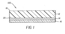
- FIG. 1 there is shown a cross-sectional representation of flexible donor element 100 used for the organic materials transfer in accordance with the current invention.
- It includes support 12 that can be a flexible polymeric sheet.
- On one surface of the support 12 it is coated with radiation-absorbing material 14, then with organic material 16. This coated surface forms transfer surface 18, and the other surface of support 12 forms non-transfer surface 20.
- Radiation-absorbing material 14 is capable of absorbing radiation in a predetermined portion of the spectrum and producing heat.
- Radiation-absorbing material 14 can be a dye such as the dyes specified in US-A-5,578,416, a pigment such as carbon, or a metal such as nickel, chromium, titanium, and so forth, or it can include a combination of materials in a single-layer or multiple-layer structure.
- Organic material 16 can be a hole-injecting material, a hole-transport material, an electron-transport material, an emissive material, a host material, or a combination of any of these materials.
- FIG. 2 is a schematic cross-sectional view of a transfer station apparatus 200 that can be used for the present invention.
- First fixture 22 is made of rigid materials. It provides mechanical support to flexible donor element 100 and substrate 10.
- First fixture 22 is provided with gasket 24, which fits into a slot that has been machined for it, that can provide a vacuum-tight seal with flexible donor element 100 when pressed against it, and pump port 26 which is connected to vacuum pump 46.
- Second fixture 28 also made of a rigid material, is provided with gasket 32 and gasket 38, each fits into a slot that has been machined for them, and pump port 36 that is connected to vacuum pump 44.
- Fixtures 22 and 28 define chamber 48.
- Vacuum pumps 44 and 46 can also be one single pump connected to pump port 26 and pump port 36 through individually controlled valves (not shown).
- Transparent window 34 is a rigid plate that is transparent to the radiation energy used for transferring organic material from flexible donor element 100 to substrate 10.
- Transparent window 34 is provided with means (not shown) to be held against second fixture 28 and pressed against gasket 32 to form a vacuum-tight seal with second fixture 28.
- Flexible donor element 100 is placed between first fixture 22 and second fixture 28 and is held together with means (not shown) to form vacuum-tight seals between flexible donor element 100 and first fixture 22, and between flexible donor element 100 and second fixture 28.
- Flexible donor element 100 and first fixture 22 forms first cavity 30; flexible donor element 100, second fixture 28, and transparent window 34 forms second cavity 40.
- Substrate 10 is mounted against first fixture 22 in first cavity 30 with means not shown in the figure, and is facing transfer surface 18 of flexible donor element 100 in a relationship that allows the transfer of organic materials from flexible donor element 100 to substrate 10.
- the gap between flexible donor element 100 and substrate 10 is kept large to facilitate pumping to ensure that the reduced pressure needed for appropriate transfer of organic material can be quickly achieved.
- FIG. 2 depicts the pump-down configuration of transfer station apparatus 200, where fixtures 22 or 28 have been moved to position, wherein flexible donor element 100 and substrate 10 have been properly loaded, cavities 30 and 40 have been formed, and evacuation of both cavities have begun.
- First cavity 30 is evacuated to achieve the desired transfer pressure.
- Second cavity 40 is evacuated to keep a small pressure differential between the two chambers to minimize the distortion of flexible donor element 100 in order to ensure that the gap between flexible donor element 100 and substrate 10 remains large. If flexible donor element 100 is pressed against substrate 10 prior to achieving the proper transfer pressure, the spacing between them will be reduced and the time to achieve proper transfer pressure will be increased. This is highly undesirable.
- FIG. 3 depicts the transfer configuration of transfer station apparatus 200.
- the pressure in second cavity 40 is increased.
- the increased pressure presses flexible donor element 100 into contact relationship with substrate 10.
- the term "contact relationship" means that the flexible donor element 100 flexible element engages the substrate 10 or spacer elements on the substrate 10. Alternatively, spacer elements such as beads can be formed on the flexible donor element 100.
- the actual gap spacing for transfer can be determined by the height of the standoffs on the substrate 10 or the flexible donor element 100. The small gap spacing is needed to achieve high-resolution transfer process.
- the radiation energy 50 is applied through transparent window 34, which is absorbed by the radiation-absorbing layer 14 to cause transfer of the organic materials from flexible donor element 100 to substrate 10.
- the pressure increase in second cavity 40 can be accomplished by venting the chamber to atmosphere, or it can be accomplished by admitting a gas from a pressurized container.
- first cavity 30 and second cavity 40 can be vented, the balance in pressure between first cavity 30 and second cavity 40 is again achieved, and the flexible donor element 100 springs back to essentially the original flatness.
- First fixture 22 and second fixture 28 can then be separated to remove the used flexible donor element 100and substrate 10. New donor and substrate pieces can then be loaded to repeat the process.
- transparent window 34 Since cavity 40 has to be evacuated, transparent window 34 needs to withstand the atmospheric pressure from outside the cavity. Transparent window 34 needs to be strong and its thickness needs to be substantial. The larger the area of the substrate to be transferred, the thicker transparent window 34 needs to be. A thick element 34 increases the working distance between radiation source 52 and flexible donor element 100, which can be difficult to achieve with certain radiation sources. If a focused scanning beam source is used, the thick transparent window 34 will also makes focusing and scanning difficult due to possible aberration of the radiation energy beam. Furthermore, it is also difficult to make large, thick transparent elements 34 with acceptable optical perfection.
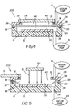
- FIG. 4 shows transfer station apparatus 300 depicting another embodiment designed according to the present invention. It is particularly suitable when large substrates are used.
- the transfer station apparatus 300 is shown in pump-down configuration. The operation of this transfer station apparatus 300 is essentially identical to that described above except transparent window 34 is replace by movable door 42.
- FIG. 5 shows this transfer station apparatus 300 in transfer configuration. After the transfer pressure has been achieved in first cavity 30 and after second cavity 40 has been vented to atmosphere, door 42 is opened exposing flexible donor element 100 to radiation energy source 52. This allows unimpeded access of flexible donor element 100 by the radiation energy beam 50. The working distance between the radiation energy source 52 and flexible donor element 100 can be reduced, and there is no longer aberration concerns.
- first cavity 30 can be vented to allow separation of first fixture 22 and second fixture 28 and removal of the used flexible donor element 100 and substrate 10.
- Door 42 can then be re-closed to second fixture 28 to allow repeating of the procedure described above.
- door 42 needs not be transparent to the radiation energy, which can simplify the construction of the apparatus.
- the organic material includes a hole-injecting material, hole-transport material, electron-transport material, emissive material, or combination thereof.
- the organic material includes at least two components, one of which is a host material.
- the radiation-absorbing material is in the form of a patterned layer selected to cause a patterned transfer of organic material.
- Apparatus for transferring organic material from a flexible donor element onto a substrate to form a layer of organic material in making one or more OLED devices comprising:
Landscapes
- Engineering & Computer Science (AREA)
- Manufacturing & Machinery (AREA)
- Electroluminescent Light Sources (AREA)
Applications Claiming Priority (2)
| Application Number | Priority Date | Filing Date | Title |
|---|---|---|---|
| US10/025,362 US6688365B2 (en) | 2001-12-19 | 2001-12-19 | Method for transferring of organic material from a donor to form a layer in an OLED device |
| US25362 | 2001-12-19 |
Publications (2)
| Publication Number | Publication Date |
|---|---|
| EP1321988A2 true EP1321988A2 (fr) | 2003-06-25 |
| EP1321988A3 EP1321988A3 (fr) | 2005-10-12 |
Family
ID=21825584
Family Applications (1)
| Application Number | Title | Priority Date | Filing Date |
|---|---|---|---|
| EP02080144A Withdrawn EP1321988A3 (fr) | 2001-12-19 | 2002-12-10 | Méthode de transfer de matériau organique à partir d'un donneur pour fabriquer une couche d'un dispositif organique luminescent |
Country Status (6)
| Country | Link |
|---|---|
| US (1) | US6688365B2 (fr) |
| EP (1) | EP1321988A3 (fr) |
| JP (1) | JP2003223991A (fr) |
| KR (1) | KR20030051379A (fr) |
| CN (1) | CN100355111C (fr) |
| TW (1) | TW579659B (fr) |
Cited By (4)
| Publication number | Priority date | Publication date | Assignee | Title |
|---|---|---|---|---|
| WO2005093814A1 (fr) * | 2004-03-02 | 2005-10-06 | Eastman Kodak Company | Feuille donneuse de diode electroluminescente organique comportant une structure d'arete rigide |
| WO2005093874A1 (fr) * | 2004-03-03 | 2005-10-06 | Eastman Kodak Company | Decoupe et fourniture de feuilles donneuses oled |
| GB2436314A (en) * | 2006-03-25 | 2007-09-26 | C R Clarke & Co | Heat transfer printing |
| US8383193B2 (en) | 2008-12-05 | 2013-02-26 | Semiconductor Energy Laboratory Co., Ltd. | Film formation method and method for manufacturing light-emitting element |
Families Citing this family (31)
| Publication number | Priority date | Publication date | Assignee | Title |
|---|---|---|---|---|
| US6703179B2 (en) * | 2002-03-13 | 2004-03-09 | Eastman Kodak Company | Transfer of organic material from a donor to form a layer in an OLED device |
| US7033711B2 (en) * | 2003-07-16 | 2006-04-25 | Eastman Kodak Company | Aperture ratio or resolution of an OLED device by limiting the edge taper region |
| US7148957B2 (en) * | 2004-06-09 | 2006-12-12 | 3M Innovative Properties Company, | Imaging system for thermal transfer |
| KR100635569B1 (ko) | 2004-09-23 | 2006-10-17 | 삼성에스디아이 주식회사 | 레이저 조사 장치 및 그를 이용한 유기 전계 발광 소자의제조 방법 |
| KR100745335B1 (ko) | 2005-08-30 | 2007-08-02 | 삼성에스디아이 주식회사 | 레이저 열전사 장치 및 이를 이용한 유기발광소자의제조방법 |
| KR100700825B1 (ko) | 2005-08-30 | 2007-03-27 | 삼성에스디아이 주식회사 | 레이저 열전사 장치 및 이를 이용한 유기 발광 다이오드의제조방법 |
| KR100700824B1 (ko) | 2005-08-30 | 2007-03-27 | 삼성에스디아이 주식회사 | 레이저 열전사 장치 및 이를 이용한 유기 발광 다이오드의제조방법 |
| KR100700829B1 (ko) | 2005-08-30 | 2007-03-27 | 삼성에스디아이 주식회사 | 레이저 열 전사 장치 및 그 장치를 이용한 레이저 열전사법 |
| KR100700837B1 (ko) | 2005-11-16 | 2007-03-28 | 삼성에스디아이 주식회사 | 레이저 열 전사 장치 및 그 장치를 이용한 레이저 열 전사법 |
| KR100700828B1 (ko) | 2005-08-30 | 2007-03-27 | 삼성에스디아이 주식회사 | 레이저 열전사법 및 이를 이용한 유기 발광소자의 제조방법 |
| US7817175B2 (en) | 2005-08-30 | 2010-10-19 | Samsung Mobile Display Co., Ltd. | Laser induced thermal imaging apparatus and fabricating method of organic light emitting diode using the same |
| JP2007062354A (ja) * | 2005-08-30 | 2007-03-15 | Samsung Sdi Co Ltd | レーザ熱転写ドナーフィルム、レーザ熱転写装置、レーザ熱転写法及び有機発光素子の製造方法 |
| KR100700826B1 (ko) | 2005-08-30 | 2007-03-27 | 삼성에스디아이 주식회사 | 레이저 열 전사 장치 및 레이저 열 전사 방법 |
| KR100711887B1 (ko) | 2005-11-04 | 2007-04-25 | 삼성에스디아이 주식회사 | 레이저 열전사 장치 |
| JP2007128845A (ja) * | 2005-11-04 | 2007-05-24 | Samsung Sdi Co Ltd | レーザ熱転写装置及びレーザ熱転写方法 |
| KR100700832B1 (ko) | 2005-11-16 | 2007-03-28 | 삼성에스디아이 주식회사 | 레이저 열 전사 장치 및 레이저 열 전사 방법 그리고 이를이용한 유기 발광 표시소자 |
| JP2007128844A (ja) * | 2005-11-04 | 2007-05-24 | Samsung Sdi Co Ltd | レーザ熱転写装置及びレーザ熱転写方法そしてこれを利用した有機発光表示素子 |
| KR100700830B1 (ko) | 2005-11-16 | 2007-03-28 | 삼성에스디아이 주식회사 | 레이저 열 전사 장치 및 레이저 열 전사 방법 |
| KR100711888B1 (ko) | 2005-11-04 | 2007-04-25 | 삼성에스디아이 주식회사 | 레이저 열전사 장치 |
| KR100700831B1 (ko) | 2005-11-16 | 2007-03-28 | 삼성에스디아이 주식회사 | 레이저 열 전사법 및 이를 이용한 유기 발광소자의제조방법 |
| KR100753569B1 (ko) * | 2005-12-30 | 2007-08-30 | 엘지.필립스 엘시디 주식회사 | 유기전계발광표시소자의 제조방법 |
| JP4837471B2 (ja) | 2006-02-20 | 2011-12-14 | 三星モバイルディスプレイ株式會社 | 有機電界発光表示装置及びその製造方法 |
| KR100784012B1 (ko) * | 2006-02-20 | 2007-12-07 | 삼성에스디아이 주식회사 | 유기 전계 발광표시장치 및 그의 제조방법 |
| KR100812027B1 (ko) | 2006-06-01 | 2008-03-10 | 삼성에스디아이 주식회사 | 레이저 열 전사 장치 및 이를 이용한 유기 발광소자의제조방법 |
| JP4797889B2 (ja) * | 2006-09-01 | 2011-10-19 | ソニー株式会社 | 転写方法 |
| US7534544B2 (en) * | 2007-10-19 | 2009-05-19 | E.I. Du Pont De Nemours And Company | Method of separating an exposed thermal transfer assemblage |
| JP5538642B2 (ja) * | 2008-04-15 | 2014-07-02 | 株式会社半導体エネルギー研究所 | 成膜方法および発光素子の作製方法 |
| US9225941B2 (en) * | 2008-08-22 | 2015-12-29 | Dish Network, L.L.C. | Systems and methods for high-bandwidth delivery of customer-specific information |
| KR101156437B1 (ko) * | 2010-01-27 | 2012-07-03 | 삼성모바일디스플레이주식회사 | 레이저 열전사 장치 및 이를 이용한 유기 발광 표시 장치의 제조방법 |
| KR101946807B1 (ko) * | 2017-04-12 | 2019-02-12 | 주식회사 서연이화 | 리얼 소재 필름을 포함하는 복합 소재 구조물의 제조 방법 |
| EP4548714A1 (fr) * | 2022-08-04 | 2025-05-07 | Reophotonics, Ltd. | Système et procédé d'impression laser à grande surface |
Family Cites Families (18)
| Publication number | Priority date | Publication date | Assignee | Title |
|---|---|---|---|---|
| FR2447819A1 (fr) * | 1979-01-30 | 1980-08-29 | Essilor Int | Procede et dispositif pour la decoration d'un quelconque substrat, en particulier monture de lunettes |
| US4670084A (en) * | 1983-06-20 | 1987-06-02 | David Durand | Apparatus for applying a dye image to a member |
| US4933042A (en) * | 1986-09-26 | 1990-06-12 | General Electric Company | Method for packaging integrated circuit chips employing a polymer film overlay layer |
| US5641372A (en) * | 1990-07-18 | 1997-06-24 | Nissha Printing Co., Ltd. | Transferring apparatus and transferring method |
| US5260714A (en) * | 1991-08-23 | 1993-11-09 | Eastman Kodak Company | Method of removing air from between superposed sheets |
| US5342817A (en) * | 1992-06-29 | 1994-08-30 | Eastman Kodak Company | Noncontact donor and receiver holder for thermal printing |
| DE4222722C2 (de) * | 1992-07-10 | 1996-08-01 | Kodak Ag | Vorrichtung zum Herstellen eines Diapositivs |
| JPH06115123A (ja) * | 1992-10-06 | 1994-04-26 | Hoei Fuji Kogyo Kk | 熱転写方法 |
| JP3401356B2 (ja) | 1995-02-21 | 2003-04-28 | パイオニア株式会社 | 有機エレクトロルミネッセンスディスプレイパネルとその製造方法 |
| US5633113A (en) * | 1995-04-14 | 1997-05-27 | Polaroid Corporation | Mass transfer imaging media and methods of making and using the same |
| US5578416A (en) | 1995-11-20 | 1996-11-26 | Eastman Kodak Company | Cinnamal-nitrile dyes for laser recording element |
| US5998085A (en) | 1996-07-23 | 1999-12-07 | 3M Innovative Properties | Process for preparing high resolution emissive arrays and corresponding articles |
| US5972780A (en) * | 1996-08-22 | 1999-10-26 | Nippon Telegraph Telephone Corporation | Thin film forming apparatus and method |
| US5800219A (en) * | 1996-12-17 | 1998-09-01 | United Technologies Automotive, Inc. | Stamped battery terminal |
| US5937272A (en) * | 1997-06-06 | 1999-08-10 | Eastman Kodak Company | Patterned organic layers in a full-color organic electroluminescent display array on a thin film transistor array substrate |
| US5851709A (en) | 1997-10-31 | 1998-12-22 | Eastman Kodak Company | Method for selective transfer of a color organic layer |
| US6114088A (en) | 1999-01-15 | 2000-09-05 | 3M Innovative Properties Company | Thermal transfer element for forming multilayer devices |
| TW504941B (en) * | 1999-07-23 | 2002-10-01 | Semiconductor Energy Lab | Method of fabricating an EL display device, and apparatus for forming a thin film |
-
2001
- 2001-12-19 US US10/025,362 patent/US6688365B2/en not_active Expired - Lifetime
-
2002
- 2002-11-12 TW TW091133147A patent/TW579659B/zh not_active IP Right Cessation
- 2002-12-10 EP EP02080144A patent/EP1321988A3/fr not_active Withdrawn
- 2002-12-18 KR KR1020020080997A patent/KR20030051379A/ko not_active Ceased
- 2002-12-18 JP JP2002366673A patent/JP2003223991A/ja not_active Withdrawn
- 2002-12-19 CN CNB021570310A patent/CN100355111C/zh not_active Expired - Lifetime
Cited By (5)
| Publication number | Priority date | Publication date | Assignee | Title |
|---|---|---|---|---|
| WO2005093814A1 (fr) * | 2004-03-02 | 2005-10-06 | Eastman Kodak Company | Feuille donneuse de diode electroluminescente organique comportant une structure d'arete rigide |
| US7238252B2 (en) | 2004-03-02 | 2007-07-03 | Eastman Kodak Company | Method of forming a OLED donor sheet having rigid edge frame |
| WO2005093874A1 (fr) * | 2004-03-03 | 2005-10-06 | Eastman Kodak Company | Decoupe et fourniture de feuilles donneuses oled |
| GB2436314A (en) * | 2006-03-25 | 2007-09-26 | C R Clarke & Co | Heat transfer printing |
| US8383193B2 (en) | 2008-12-05 | 2013-02-26 | Semiconductor Energy Laboratory Co., Ltd. | Film formation method and method for manufacturing light-emitting element |
Also Published As
| Publication number | Publication date |
|---|---|
| EP1321988A3 (fr) | 2005-10-12 |
| CN100355111C (zh) | 2007-12-12 |
| KR20030051379A (ko) | 2003-06-25 |
| TW200303695A (en) | 2003-09-01 |
| JP2003223991A (ja) | 2003-08-08 |
| US20030113656A1 (en) | 2003-06-19 |
| CN1427653A (zh) | 2003-07-02 |
| US6688365B2 (en) | 2004-02-10 |
| TW579659B (en) | 2004-03-11 |
Similar Documents
| Publication | Publication Date | Title |
|---|---|---|
| US6688365B2 (en) | Method for transferring of organic material from a donor to form a layer in an OLED device | |
| JP4971723B2 (ja) | 有機発光表示装置の製造方法 | |
| US7648944B2 (en) | Transfer method and transfer apparatus | |
| US8298340B2 (en) | Organic thin film deposition device, organic EL element manufacturing device, and organic thin film deposition method | |
| KR100718555B1 (ko) | 잉크젯 프린팅과 저분자 유기증착 방법을 겸용하는 대면적 유기 박막 증착장치 | |
| JP4701815B2 (ja) | 成膜装置 | |
| US20190036027A1 (en) | A shadow mask with tapered openings formed by double electroforming | |
| US8864938B2 (en) | Vacuum peeling apparatus and method | |
| JP2014186868A (ja) | 転写装置、転写方法、及びデバイス製造方法 | |
| KR20060081410A (ko) | Oled에 유기 층을 형성하는 방법 | |
| US7317469B2 (en) | Laser induced thermal imaging apparatus | |
| TWI406442B (zh) | 有機電激發光元件製造方法及有機電激發光元件製造裝置 | |
| WO2017132908A1 (fr) | Masque perforé à ouvertures coniques formé par double électroformage à l'aide de photorésines positives/négatives | |
| US20210214834A1 (en) | Shadow mask with tapered openings formed by double electroforming with reduced internal stresses | |
| KR102456282B1 (ko) | 진공 장치, 증착 장치 및 게이트 밸브 | |
| JP2008223067A (ja) | 成膜用マスク部材、成膜用マスク部材の製造方法、マスク成膜方法、および成膜装置 | |
| JP4797889B2 (ja) | 転写方法 | |
| US7238252B2 (en) | Method of forming a OLED donor sheet having rigid edge frame | |
| US7032285B2 (en) | Mounting an OLED donor sheet to frames | |
| KR100670375B1 (ko) | 박막 증착용 마스크, 박막 증착 방법 및 유기 발광표시장치의 제조방법 | |
| KR100696543B1 (ko) | 기판 접합장치 | |
| WO2025163662A1 (fr) | Substrat source réutilisable pour la formation de motifs et le transfert de couches organiques fonctionnelles vers des dispositifs optoélectroniques multicouches | |
| JP2005310635A (ja) | 蒸着マスク、蒸着マスク製造方法、有機薄膜成膜方法 | |
| KR101901249B1 (ko) | 전사 장치 및 방법 | |
| CN113637940A (zh) | 一种能够提高蒸镀品质的oled蒸镀用掩膜板及其应用方法 |
Legal Events
| Date | Code | Title | Description |
|---|---|---|---|
| PUAI | Public reference made under article 153(3) epc to a published international application that has entered the european phase |
Free format text: ORIGINAL CODE: 0009012 |
|
| AK | Designated contracting states |
Designated state(s): AT BE BG CH CY CZ DE DK EE ES FI FR GB GR IE IT LI LU MC NL PT SE SI SK TR |
|
| AX | Request for extension of the european patent |
Extension state: AL LT LV MK RO |
|
| PUAL | Search report despatched |
Free format text: ORIGINAL CODE: 0009013 |
|
| AK | Designated contracting states |
Kind code of ref document: A3 Designated state(s): AT BE BG CH CY CZ DE DK EE ES FI FR GB GR IE IT LI LU MC NL PT SE SI SK TR |
|
| AX | Request for extension of the european patent |
Extension state: AL LT LV MK RO |
|
| RIC1 | Information provided on ipc code assigned before grant |
Ipc: 7B 41M 5/38 B Ipc: 7H 01L 51/40 A |
|
| 17P | Request for examination filed |
Effective date: 20060311 |
|
| AKX | Designation fees paid |
Designated state(s): DE FR GB |
|
| 17Q | First examination report despatched |
Effective date: 20080530 |
|
| STAA | Information on the status of an ep patent application or granted ep patent |
Free format text: STATUS: THE APPLICATION IS DEEMED TO BE WITHDRAWN |
|
| 18D | Application deemed to be withdrawn |
Effective date: 20081010 |