EP1322146A1 - Methode zur elektrochemische Abscheidung von Lötbällen auf eine organische Leiterplatte - Google Patents
Methode zur elektrochemische Abscheidung von Lötbällen auf eine organische Leiterplatte Download PDFInfo
- Publication number
- EP1322146A1 EP1322146A1 EP01310551A EP01310551A EP1322146A1 EP 1322146 A1 EP1322146 A1 EP 1322146A1 EP 01310551 A EP01310551 A EP 01310551A EP 01310551 A EP01310551 A EP 01310551A EP 1322146 A1 EP1322146 A1 EP 1322146A1
- Authority
- EP
- European Patent Office
- Prior art keywords
- copper
- tin
- thin metal
- solder
- metal layer
- Prior art date
- Legal status (The legal status is an assumption and is not a legal conclusion. Google has not performed a legal analysis and makes no representation as to the accuracy of the status listed.)
- Withdrawn
Links
Images


Classifications
-
- H—ELECTRICITY
- H05—ELECTRIC TECHNIQUES NOT OTHERWISE PROVIDED FOR
- H05K—PRINTED CIRCUITS; CASINGS OR CONSTRUCTIONAL DETAILS OF ELECTRIC APPARATUS; MANUFACTURE OF ASSEMBLAGES OF ELECTRICAL COMPONENTS
- H05K3/00—Apparatus or processes for manufacturing printed circuits
- H05K3/30—Assembling printed circuits with electric components, e.g. with resistors
- H05K3/32—Assembling printed circuits with electric components, e.g. with resistors electrically connecting electric components or wires to printed circuits
- H05K3/34—Assembling printed circuits with electric components, e.g. with resistors electrically connecting electric components or wires to printed circuits by soldering
- H05K3/3465—Application of solder
- H05K3/3473—Plating of solder
-
- H—ELECTRICITY
- H10—SEMICONDUCTOR DEVICES; ELECTRIC SOLID-STATE DEVICES NOT OTHERWISE PROVIDED FOR
- H10W—GENERIC PACKAGES, INTERCONNECTIONS, CONNECTORS OR OTHER CONSTRUCTIONAL DETAILS OF DEVICES COVERED BY CLASS H10
- H10W70/00—Package substrates; Interposers; Redistribution layers [RDL]
- H10W70/01—Manufacture or treatment
- H10W70/05—Manufacture or treatment of insulating or insulated package substrates, or of interposers, or of redistribution layers
-
- H—ELECTRICITY
- H10—SEMICONDUCTOR DEVICES; ELECTRIC SOLID-STATE DEVICES NOT OTHERWISE PROVIDED FOR
- H10W—GENERIC PACKAGES, INTERCONNECTIONS, CONNECTORS OR OTHER CONSTRUCTIONAL DETAILS OF DEVICES COVERED BY CLASS H10
- H10W72/00—Interconnections or connectors in packages
- H10W72/071—Connecting or disconnecting
- H10W72/072—Connecting or disconnecting of bump connectors
-
- H—ELECTRICITY
- H10—SEMICONDUCTOR DEVICES; ELECTRIC SOLID-STATE DEVICES NOT OTHERWISE PROVIDED FOR
- H10W—GENERIC PACKAGES, INTERCONNECTIONS, CONNECTORS OR OTHER CONSTRUCTIONAL DETAILS OF DEVICES COVERED BY CLASS H10
- H10W90/00—Package configurations
- H10W90/701—Package configurations characterised by the relative positions of pads or connectors relative to package parts
-
- H—ELECTRICITY
- H05—ELECTRIC TECHNIQUES NOT OTHERWISE PROVIDED FOR
- H05K—PRINTED CIRCUITS; CASINGS OR CONSTRUCTIONAL DETAILS OF ELECTRIC APPARATUS; MANUFACTURE OF ASSEMBLAGES OF ELECTRICAL COMPONENTS
- H05K2203/00—Indexing scheme relating to apparatus or processes for manufacturing printed circuits covered by H05K3/00
- H05K2203/05—Patterning and lithography; Masks; Details of resist
- H05K2203/0502—Patterning and lithography
- H05K2203/054—Continuous temporary metal layer over resist, e.g. for selective electroplating
-
- H—ELECTRICITY
- H05—ELECTRIC TECHNIQUES NOT OTHERWISE PROVIDED FOR
- H05K—PRINTED CIRCUITS; CASINGS OR CONSTRUCTIONAL DETAILS OF ELECTRIC APPARATUS; MANUFACTURE OF ASSEMBLAGES OF ELECTRICAL COMPONENTS
- H05K3/00—Apparatus or processes for manufacturing printed circuits
- H05K3/30—Assembling printed circuits with electric components, e.g. with resistors
- H05K3/32—Assembling printed circuits with electric components, e.g. with resistors electrically connecting electric components or wires to printed circuits
- H05K3/34—Assembling printed circuits with electric components, e.g. with resistors electrically connecting electric components or wires to printed circuits by soldering
- H05K3/3452—Solder masks
Definitions
- This invention generally relates to the electronic packages, particularly to flip chip packages, more particularly to flip chip joints and board to board solder joints formed by electroplated solder on the organic circuit boards.
- the flip chip devices Since the introduction of the flip chip technology by IBM in the early 1960s, the flip chip devices have been mounted on an expensive ceramic substrate where the thermal expansion mismatch between the silicon chip and the ceramic substrate is less critical. In comparison with wire bonding technology, the flip chip technology is better able to offer higher packaging density (lower device profile) and higher electrical performance (shorter possible leads and lower inductance). On this basis, the flip chip technology has been industrially practiced for the past 40 years using high-temperature solder (controlled-collapse chip connection, C4) on ceramic substrates. However, in recent years, driven by the demand of high-density, high-speed and low-cost semiconductor devices for the trend of miniaturization of modem electronic products, the flip chip devices mounted on a low-cost organic circuit board (e.g.
- the top surface of the semiconductor integrated circuit (IC) chip has an array of electrical contact pads.
- the organic circuit board has also a corresponding grid of contacts.
- the low-temperature solder bumps or other conductive adhesive material are placed and properly aligned in between the chip and circuit board.
- the chip is flipped upside down and mounted on the circuit board, in which the solder bumps or conductive adhesive material provide electrical input/output (I/O) and mechanical interconnects between the chip and circuit board.
- I/O electrical input/output
- an organic underfill encapsulant may be further dispensed into the gap between the chip and circuit board to constrain the thermal mismatch and lower the stress on the solder joints.
- the metal bumps such as solder bumps, gold bumps or copper bumps
- the bumps can be any shape, such as stud bumps, ball bumps, columnar bumps, or others.
- the corresponding solder bumps typically using a low-temperature solder, are also formed on the contact pads of the circuit board.
- the chip is bonded to the circuit board by means of the solder joints. After dispensing of an underfill encapsulant, the flip chip device is thus constructed.
- the typical examples of the flip chip devices using solder joints are shown in Figs. 1 and 2. Fig.
- the metal bumps 101 are formed on the electrode pads 102 of the chip 103.
- the presolder bumps 104 made of low-temperature solder are formed on the contact pads 105 of the organic circuit board 106.
- the solder joints 107 are formed at a reflow temperature sufficient to melt and reflow the presolder bumps 104. After dispensing of an underfill encapsulant 107 into the gap between the chip 103 and circuit board 106, the flip chip device 100 is thus accomplished.
- Fig. 2 shows another example of the typical flip chip devices without using presolder bumps.
- the solder bumps 201 are formed on the electrode pads 202 of the chip 203.
- the chip 203 is bonded to the circuit board 204 at a reflow temperature, in which the solder joints 205 are formed at the contact pads 206. After dispensing of an underfill encapsulant 207 into the gap between the chip 203 and circuit board 204, the flip chip device 200 is thus accomplished.
- solder bumps deposited by electroplating offers the ability to further reduce bump pitch down to below 0.15 millimeter.
- the prior proposals in relation to electroplate bumps on the circuit board for flip chip bonding can be found in U.S. Pat. Nos. 5391514 (T. P. Gall et al .) and 5480835 (K. G. Hoebener et al .).
- eletroplate solder bumping on the circuit board offers finer bump pitch over stencil printing, it presents several challenges for initial implementation. For example, the solder mask layer should not be damaged during the fabrication process of solder bumps. Also, the plating and bump height uniformity should also be established. These issues were not detailed in either U.S. Pat. No. 5391514 or 5480835.
- Another objective of this invention is to adopt a physical vapor deposition method for forming the metal seed layer.
- Another further objective of this invention is to adopt a chemical vapor deposition method for forming the metal seed layer.
- Another further objective of the present invention is to adopt an electroless plating method for forming the metal seed layer, wherein the surfaces of said solder mask layer and said pad are coated with aqueous solutions, which at least contain copper ions, followed by reduction of said copper ions to form the catalytic copper. With assistance of the catalytic copper, the metal seed layer can then be formed by the electroless plating method.
- Another further objective of the present invention is to adopt an electroplating method for forming the metal seed layer, wherein the surfaces of said solder mask layer and said pad are coated with aqueous solutions, which at least contain copper ions, followed by reduction of said copper ions to form the catalytic copper.
- a first thin metal layer can thus be formed by the electroless plating method.
- the second thin metal layer can then be formed by the electroplating method.
- the metal seed layer is a combination of the first and second thin metal layers.
- an organic circuit board including a surface bearing electrical circuitry which includes at least one contact pad.
- a solder mask layer that is placed on the board surface and patterned to expose the pad.
- a metal seed layer is deposited by physical vapor deposition, chemical vapor deposition, electroless plating with the use of catalytic copper, or electroplating with the use of catalytic copper, over the board surface.
- a resist layer with at least an opening located at the pad is formed over the metal seed layer.
- a solder material is then formed in the opening by electroplating. Finally, the resist and the metal seed layer beneath the resist are removed.
- the invention provides an electroplating process for fabricating solder bumps on an organic circuit board, which is able to form solder bumps with good plating uniformity but without significantly damaging solder mask layers.
- the method is detailed as follows. Like numbers refer to like elements throughout. However, the figures are simply illustrative of the process, and are not drawn to scale, i.e. they do not reflect the actual dimensions or features of the various layers in the chip package structure.
- an organic circuit board 305 which has the contact pads 310 on its surface.
- the insulative layers used for said organic circuit board 305 may be made of an organic material or a fiber-reinforced organic material or a particle-reinforced organic material, etc., for example, epoxy resin, polyimide, bismeleimide triazine, cyanate ester, polybenzocyclobutene, or glass fiber composite thereof, etc.
- Said contact pad 310 is formed typically from a metal material, such as copper.
- a popular barrier layer 315 includes an adhesive layer of nickel and a protective layer of gold may be formed to cover said pad 310.
- said barrier layer 315 may also be made of nickel, palladium, silver, tin, nickel/palladium, chromium/titanium, palladium/gold, or nickel/palladium/gold, etc., which can be made by electoplating, electroless plating, or physical vapor deposition, etc.
- a solder mask layer 320 is finally deposited on the surface of said circuit board 305 to protect the circuitry and provide insulation.
- a conductive seed layer formed on the non-conductive surface is required to initiate the electroplating.
- the seed layer is prevailingly formed by electroless deposition in the conventional manufacturing industry of organic circuit boards.
- the surface must be immersed in a chemical solution first to form a catalytic surface (e.g. sensitizer, including stannous chloride, titanium chloride, etc.; and activator, including acidified palladium chloride, acidified gold chloride, acidified silver chloride, etc.) and then again immersed in an electroless plating solution to form a conductive seed layer.
- a catalytic surface e.g. sensitizer, including stannous chloride, titanium chloride, etc.; and activator, including acidified palladium chloride, acidified gold chloride, acidified silver chloride, etc.
- electroplating can thus be carried out to form metal bumps.
- the use of electroless plating for formation of the seed layer on the organic circuit substrate has several disadvantages.
- One significant problem is that the organic circuit board exposed to the chemical solutions, i.e. sensitizer solution, activation solution, and electroless solution, will significantly damage (corrosively) the solder mask layer and thus cause the reliability problem of the circuit board.
- sensitizer and activation solutions commonly contain a vast amount of chloride ions, which may penetrate into the solder mask layer and remain in the solder mask layer after immersion and also result in the reliability problem of the organic circuit board.
- the noble metal e.g. palladium, gold, and silver, etc.
- the present invention proposes a method to form a metal seed layer without dipping the organic circuit board in any chemical solutions.
- the metal layer used as the seed layer is directly deposited on the surfaces of the organic circuit board by physical vapor deposition (PVD) or chemical vapor deposition (CVD), such as sputtering, evaporation, arc vapor deposition, ion beam sputtering, laser ablation deposition, plasma enhanced CVD, metallorganic CVD, etc.
- PVD physical vapor deposition
- CVD chemical vapor deposition
- sputtering evaporation
- arc vapor deposition ion beam sputtering
- laser ablation deposition ion beam sputtering
- plasma enhanced CVD metallorganic CVD
- a metal seed layer 325 is deposited on the surface of said circuit board 305, by PVD or CVD.
- a resist layer 330 with the openings 335 is then formed and covers said seed layer 325, as shown in Fig. 3C, and subsequently the electroplate solder 340 is formed in said opening 335.
- both said resist 330 and said metal seed layer 325 beneath said resist 330 are then removed.
- the solder bumps 345 are formed on said contact pads 310.
- said metal seed layer 325 may be made of a metal or an alloy or made of multilayer of metals, such as copper, tin, cobalt, tin-lead alloy, chromium-copper alloy, titanium/nickel (bi-metal), tin/copper, chromium/chromium-copper alloy/copper, or nickel/tin/copper multilayer etc.
- the noble metal such as gold, silver, palladium, platinum, molybdenum, and tantalum, etc., should be avoided to be used as a part of said seed layer 325, since those metals are difficult to be removed without significantly damaging said solder mask layer 320 during the etching step.
- the thickness of said seed layer 325 is better less than 0.1 millimeter, however preferably between 0.0001 millimeter and 0.005 millimeter.
- said seed layer 325 does not completely dissolve into said solder bumps and still exists after the reflow process, such as said seed layer 325 made of nickel and said solder bumps made of tin or tin-lead alloy.
- Fig. 3E in which said seed layer 325 does not completely dissolve into said solder bumps and still exists after the reflow process, such as said seed layer 325 made of nickel and said solder bumps made of tin or tin-lead alloy.
- Fig. 3E in which said seed layer 325 does not completely dissolve into said solder bumps and still exists after the reflow process, such as said seed layer 325 made of nickel and said solder bumps made of tin or tin-lead alloy.
- Fig. 3E in which said seed layer 325 does not completely dissolve into said solder bumps and still exists after the
- said seed layer 325 does dissolve completely into said solder bumps 345 and said seed layer 325 disappears after the reflow process, such as said seed layer 325 made of tin and said solder bumps 345 made of tin-lead or tin-copper alloy.
- the tin/copper bi-layer as said seed layer 325 is a good choice.
- said copper completely covering said tin layer is used to prevent oxidation of said tin layer during the resist patterning step.
- said copper surface may be roughened for obtaining good adhesion between said copper and said resist layer 330.
- said copper is removed in said opening 335 of said resist 330, and subsequently in plating, said tin is used to provide the plating current paths and a clean surface for electroplate solder.
- said tin could dissolve into said solder bumps 345, the composition of said solder bumps 345 could thus be easily controlled. Furthermore, once nickel is chosen and used as said barrier layer 315, said tin is able to function to block the contact between said nickel and the plating solution during plating to protect the plating solution, since commonly nickel may dissolve into the plating solution and destroy the performance of the plating solution.
- the single tin layer as said seed layer 325 is also a good choice.
- said resist 330 is directly placed on said tin layer (i. e. seed layer) 325.
- said tin surface in said opening 335 of said resist 330 is pre-cleaned, and subsequently in plating, said tin layer is used to provide the plating current paths and a clean surface for electroplate solder.
- the thickness of said tin layer in said opening 335 is better larger than 0.0001 mm after the pre-cleaning step.
- the above method can also be applied.
- said solder bumps 345 are formed in direct contact with said contact pad 310.
- said solder material 340 is an alloy made by the mixture of the elements selected from the group consisting of lead, tin, silver, copper, bismuth, antimony, zinc, nickel, aluminum, magnesium, indium, tellurium, and gallium, etc.
- a cleaning process e.g. ultrasonic cleaning, may be conducted to remove the flux residues.
- thinner said seed layer 325 is found better. Since the thinner seed layer can be removed sooner in the etching solution, the time required for said organic circuit board 305 immersed in said etching solution could be shortened. In such a case, the damages to said solder mask layer 320 and electroplate solder 340 by said etching solution will be lowered down to an acceptable low level. In another respect, at the reflow process, when said seed layer 325, such as tin, is dissolvable in said electroplate solder 340, such as tin-lead or tin-copper solder, said thinner seed layer 325 would make a smaller amount of tin dissolved in said solder bump 345.
- said seed layer 325 such as tin
- said alloy composition of said solder bump 345 would become much easier to be controlled.
- said seed layer 0.0002 to 0.005 millimeter works well.
- the selection of said etching solution composition has been long recognized in the art and can be referred to some popular metallography books, for example, "Metallographic etching", Gunter Petzow, American Society for Metals, Metals Park, Ohio, (1978).
- said seed layer 325 can also be formed by an electroless plating or electroplating method, wherein the catalytic metal does not use noble metal but uses copper as the catalytic metal.
- the catalytic metal does not use noble metal but uses copper as the catalytic metal.
- the typical examples for forming such a catalytic copper on a non-conductive surface can be found in the U. S. Pat. Nos. 3,993,491 and 3,993,848, the disclosures of which are hereby incorporated by reference.
- said metal seed layer 325 could thus be formed by electroless plating.
- said metal seed layer 325 can also be formed by electroplating after a short time period of electroless plating.
- the catalytic copper is formed on the non-conductive surface, and then a first thin metal layer is formed by electroplating over said catalytic copper. Afterwards, a second thin metal layer is formed over said first thin metal layer.
- said seed layer 325 is a combination of said first and second thin layers. Also, the damages to said solder mask layer 320 could be mitigated, since the catalytic copper (which is not noble metal) can be easily removed in said etching solution.
- said electroplate solder bumps 345 formed on an organic circuit board 305 can thus be constructed, as shown in Figs. 3E, 3F, and 3G.
- said solder mask layer 320 is not limited to cover a portion of said contact pad 310 surface. As shown in Fig. 4A, said solder mask layer 320 is deposited on the surface of said organic circuit board 305 but does not cover any portion of said contact pad 310 surface. In turn, said seed layer 325 and resist 330 with said openings 335 (not shown) are formed. Subsequently, said electroplate solder 340 is formed in said opening 335. After removal of said resist 330 and seed layer 325 beneath said resist 330, said solder bumps 345 can be formed by the reflow process. There are also two phenomena that could be observed, depending on the solubility of said seed layer 325 in said solder bumps.
- said contact pad 310 is not limited to any configuration and size. As shown in Fig. 5A, the upper most three circuit layers 350 of said organic circuit board 305 are only illustrated. As can be observed, the surface of the contact pad 310a and the surface 355 of the insulative layer 360 are at the same plane. A solder mask layer 320 is deposited and patterned to expose said contact pad 310a. The vertical circuit lines 365 are commonly formed by the so-called "stacked via" technique. In such a case, the electroplate solder bumps 345 can also be made on said contact pad 310a by means of the method proposed in the present invention.
- said electroplate solder bumps 345 can be applied for forming flip chip joints.
- an IC chip 370 with the electrode pads 375 is attached to said organic circuit board 305.
- a flip chip joint 380 can be formed in between said contact pad 310 and electrode pad 375, as illustrated in Fig. 6B.
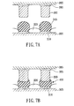
- said electroplate solder bumps 345 can be applied for forming flip chip joints with the use the metal bumps on the IC chip.
- an IC chip 385 with a metal bump 390 on each electrode pad 395 is attached to said organic circuit board 305.
- a flip chip joint 405 can be formed in between said contact pad 310 and electrode pad 395, as illustrated in Fig. 7B.
- said metal bumps 390 can be made of a metal or an alloy or a stacking of several metals, such as solder bumps, gold bumps, copper bumps, or copper posts covered with solder caps, etc. and can be any shape, such as stud bumps, ball bumps, columnar bumps, or others.
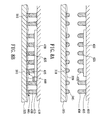
- said electroplate solder bumps 345 can be applied for forming flip chip joints and board to board solder joints.
- a circuit board 410 which can be an organic circuit board or a ceramic circuit board, has the contact pads 415 on its surface and an IC chip 420 with the electrode pads 425 is bonded to the surface of said circuit board 410.
- a metal bump 430 is formed on each contact pad 415 and the other metal bump 435 is formed on each electrode pad 425.
- Said circuit board 410 is then attached to said organic circuit board 305.
- a flip chip joint 440 in between said contact pad 310 and electrode pad 425 and a board to board solder joint 445 in between said contact pad 310 and contact pad 415 can be formed, as illustrated in Fig. 8B.
- said metal bumps 430 can be made of a metal or an alloy or a stacking of several metals, such as solder bumps, gold bumps, copper bumps, or copper posts covered with solder caps, etc. and can be any shape, such as stud bumps, ball bumps, columnar bumps, or others.
Landscapes
- Engineering & Computer Science (AREA)
- Manufacturing & Machinery (AREA)
- Microelectronics & Electronic Packaging (AREA)
- Wire Bonding (AREA)
Priority Applications (1)
| Application Number | Priority Date | Filing Date | Title |
|---|---|---|---|
| EP01310551A EP1322146A1 (de) | 2001-12-18 | 2001-12-18 | Methode zur elektrochemische Abscheidung von Lötbällen auf eine organische Leiterplatte |
Applications Claiming Priority (1)
| Application Number | Priority Date | Filing Date | Title |
|---|---|---|---|
| EP01310551A EP1322146A1 (de) | 2001-12-18 | 2001-12-18 | Methode zur elektrochemische Abscheidung von Lötbällen auf eine organische Leiterplatte |
Publications (1)
| Publication Number | Publication Date |
|---|---|
| EP1322146A1 true EP1322146A1 (de) | 2003-06-25 |
Family
ID=8182545
Family Applications (1)
| Application Number | Title | Priority Date | Filing Date |
|---|---|---|---|
| EP01310551A Withdrawn EP1322146A1 (de) | 2001-12-18 | 2001-12-18 | Methode zur elektrochemische Abscheidung von Lötbällen auf eine organische Leiterplatte |
Country Status (1)
| Country | Link |
|---|---|
| EP (1) | EP1322146A1 (de) |
Cited By (6)
| Publication number | Priority date | Publication date | Assignee | Title |
|---|---|---|---|---|
| US7326414B2 (en) | 2003-09-10 | 2008-02-05 | Warner-Lambert Company Llc | Antibodies to M-CSF |
| EP2120262A1 (de) * | 2008-05-16 | 2009-11-18 | Phoenix Precision Technology Corporation | Struktur für Verkapselungssubstrat und Verfahren zu ihrer Herstellung |
| EP2180770A1 (de) * | 2008-10-21 | 2010-04-28 | Atotech Deutschland Gmbh | Verfahren zur Formung von Lötablagerungen auf Substraten |
| WO2010046235A1 (en) * | 2008-10-21 | 2010-04-29 | Atotech Deutschland Gmbh | Method to form solder deposits on substrates |
| EP3327802A1 (de) * | 2016-11-24 | 2018-05-30 | Valeo Iluminacion | Verfahren zur erzeugung einer leiterbahn und dichtungssystem |
| WO2018115408A1 (en) | 2016-12-23 | 2018-06-28 | Atotech Deutschland Gmbh | Method of forming a solderable solder deposit on a contact pad |
Citations (5)
| Publication number | Priority date | Publication date | Assignee | Title |
|---|---|---|---|---|
| JPH02114694A (ja) * | 1988-10-25 | 1990-04-26 | Mitsubishi Electric Corp | 回路基板の製造方法 |
| US5454930A (en) * | 1991-08-15 | 1995-10-03 | Learonal Japan Inc. | Electrolytic copper plating using a reducing agent |
| US5789142A (en) * | 1996-01-16 | 1998-08-04 | Motorola, Inc. | Solder mask system |
| DE19716044A1 (de) * | 1997-04-17 | 1998-10-22 | Univ Dresden Tech | Verfahren zur Herstellung von festen Lotdepots auf Leiterplatten |
| WO2001020647A2 (en) * | 1999-09-17 | 2001-03-22 | Nutool, Inc. | Novel chip interconnect and packaging deposition methods and structures |
-
2001
- 2001-12-18 EP EP01310551A patent/EP1322146A1/de not_active Withdrawn
Patent Citations (5)
| Publication number | Priority date | Publication date | Assignee | Title |
|---|---|---|---|---|
| JPH02114694A (ja) * | 1988-10-25 | 1990-04-26 | Mitsubishi Electric Corp | 回路基板の製造方法 |
| US5454930A (en) * | 1991-08-15 | 1995-10-03 | Learonal Japan Inc. | Electrolytic copper plating using a reducing agent |
| US5789142A (en) * | 1996-01-16 | 1998-08-04 | Motorola, Inc. | Solder mask system |
| DE19716044A1 (de) * | 1997-04-17 | 1998-10-22 | Univ Dresden Tech | Verfahren zur Herstellung von festen Lotdepots auf Leiterplatten |
| WO2001020647A2 (en) * | 1999-09-17 | 2001-03-22 | Nutool, Inc. | Novel chip interconnect and packaging deposition methods and structures |
Non-Patent Citations (3)
| Title |
|---|
| "SOLDER BUMP-MAKING PROCESS", IBM TECHNICAL DISCLOSURE BULLETIN, IBM CORP. NEW YORK, US, VOL. 32, NR. 3B, PAGE(S) 36-37, ISSN: 0018-8689, XP000029934 * |
| PATENT ABSTRACTS OF JAPAN vol. 014, no. 338 (E - 0954) 20 July 1990 (1990-07-20) * |
| SHACHAM-DIAMAND Y; ET AL: "THE CHARACTERIZATION OF ELECTROLESS COPPER DEPOSITION FROM AN ALKALI FREE SOLUTION", ELECTROCHEMICAL SOCIETY PROCEEDINGS, 1 October 1994 (1994-10-01), PENNINGTON, NJ, US, pages 136 - 145, XP000937895 * |
Cited By (14)
| Publication number | Priority date | Publication date | Assignee | Title |
|---|---|---|---|---|
| US8188249B2 (en) | 2003-09-10 | 2012-05-29 | Amgen Fremont Inc. | Nucleic acid molecules encoding antibodies to M-CSF |
| US7592430B2 (en) | 2003-09-10 | 2009-09-22 | Amgen Fremont | Antibodies to M-CSF |
| US7326414B2 (en) | 2003-09-10 | 2008-02-05 | Warner-Lambert Company Llc | Antibodies to M-CSF |
| US10280219B2 (en) | 2003-09-10 | 2019-05-07 | Amgen Fremont Inc. | Antibodies to M-CSF |
| US7728113B2 (en) | 2003-09-10 | 2010-06-01 | Amgen Fremont Inc. | Methods of treating arthritic conditions with antibodies to M-CSF |
| US9718883B2 (en) | 2003-09-10 | 2017-08-01 | Amgen Fremont Inc. | Antibodies to M-CSF |
| EP2120262A1 (de) * | 2008-05-16 | 2009-11-18 | Phoenix Precision Technology Corporation | Struktur für Verkapselungssubstrat und Verfahren zu ihrer Herstellung |
| EP2180770A1 (de) * | 2008-10-21 | 2010-04-28 | Atotech Deutschland Gmbh | Verfahren zur Formung von Lötablagerungen auf Substraten |
| US8507376B2 (en) | 2008-10-21 | 2013-08-13 | Atotech Deutschland Gmbh | Method to form solder deposits on substrates |
| CN102187749A (zh) * | 2008-10-21 | 2011-09-14 | 埃托特克德国有限公司 | 用于在衬底上形成焊料沉积物的方法 |
| WO2010046235A1 (en) * | 2008-10-21 | 2010-04-29 | Atotech Deutschland Gmbh | Method to form solder deposits on substrates |
| EP3327802A1 (de) * | 2016-11-24 | 2018-05-30 | Valeo Iluminacion | Verfahren zur erzeugung einer leiterbahn und dichtungssystem |
| WO2018115408A1 (en) | 2016-12-23 | 2018-06-28 | Atotech Deutschland Gmbh | Method of forming a solderable solder deposit on a contact pad |
| US11032914B2 (en) | 2016-12-23 | 2021-06-08 | Atotech Deutschland Gmbh | Method of forming a solderable solder deposit on a contact pad |
Similar Documents
| Publication | Publication Date | Title |
|---|---|---|
| US7098126B2 (en) | Formation of electroplate solder on an organic circuit board for flip chip joints and board to board solder joints | |
| KR100857727B1 (ko) | 구리 집적 회로에서의 상호 접속 | |
| KR100454381B1 (ko) | 반도체 장치 및 그 제조 방법 | |
| JP4334647B2 (ja) | 半導体デバイス上に導電性バンプを形成する方法 | |
| US6153940A (en) | Core metal soldering knob flip-chip technology | |
| JP5113177B2 (ja) | 半導体素子およびその製造方法、ならびにその半導体素子を実装する実装構造体 | |
| US20040084206A1 (en) | Fine pad pitch organic circuit board for flip chip joints and board to board solder joints and method | |
| JP4685834B2 (ja) | 集積回路デバイス | |
| US20090174071A1 (en) | Semiconductor device including electrically conductive bump and method of manufacturing the same | |
| US8314500B2 (en) | Interconnections for flip-chip using lead-free solders and having improved reaction barrier layers | |
| KR100772920B1 (ko) | 솔더 범프가 형성된 반도체 칩 및 제조 방법 | |
| US20080136019A1 (en) | Solder Bump/Under Bump Metallurgy Structure for High Temperature Applications | |
| KR20010098699A (ko) | 납 없는 범프 배선의 형성 방법 | |
| US7041591B1 (en) | Method for fabricating semiconductor package substrate with plated metal layer over conductive pad | |
| KR20040012877A (ko) | 반도체 장치 및 그 제조 방법 | |
| CN1291468C (zh) | 用于制造互连结构的方法和装置 | |
| JP2007317979A (ja) | 半導体装置の製造方法 | |
| KR20200035197A (ko) | 반도체 장치 및 그 제조 방법 | |
| CN1169413C (zh) | 在有机电路板上进行电镀焊锡的方法 | |
| EP1322146A1 (de) | Methode zur elektrochemische Abscheidung von Lötbällen auf eine organische Leiterplatte | |
| JP4603383B2 (ja) | 配線基板及び半導体装置並びにそれらの製造方法 | |
| KR100455678B1 (ko) | 반도체 플립칩 패키지를 위한 솔더 범프 구조 및 그 제조방법 | |
| TW545098B (en) | Fine pad pitch organic circuit board with plating solder and method for fabricating the same | |
| KR20020060307A (ko) | 솔더 범프의 형성 방법 | |
| KR100726059B1 (ko) | 플립칩 조인트 및 보드대면형 솔더 조인트를 위한유기회로보드 상의 전기도금 솔더 형성 |
Legal Events
| Date | Code | Title | Description |
|---|---|---|---|
| PUAI | Public reference made under article 153(3) epc to a published international application that has entered the european phase |
Free format text: ORIGINAL CODE: 0009012 |
|
| AK | Designated contracting states |
Designated state(s): AT BE CH CY DE DK ES FI FR GB GR IE IT LI LU MC NL PT SE TR |
|
| AX | Request for extension of the european patent |
Extension state: AL LT LV MK RO SI |
|
| 17P | Request for examination filed |
Effective date: 20031208 |
|
| AKX | Designation fees paid |
Designated state(s): DE FR GB NL SE |
|
| 17Q | First examination report despatched |
Effective date: 20070814 |
|
| STAA | Information on the status of an ep patent application or granted ep patent |
Free format text: STATUS: THE APPLICATION IS DEEMED TO BE WITHDRAWN |
|
| 18D | Application deemed to be withdrawn |
Effective date: 20090122 |