EP1323281B1 - Vorrichtung und verfahren zur verbesserung des niederfrequenten betriebs von mobilkommunikationsantennen - Google Patents
Vorrichtung und verfahren zur verbesserung des niederfrequenten betriebs von mobilkommunikationsantennen Download PDFInfo
- Publication number
- EP1323281B1 EP1323281B1 EP01958358A EP01958358A EP1323281B1 EP 1323281 B1 EP1323281 B1 EP 1323281B1 EP 01958358 A EP01958358 A EP 01958358A EP 01958358 A EP01958358 A EP 01958358A EP 1323281 B1 EP1323281 B1 EP 1323281B1
- Authority
- EP
- European Patent Office
- Prior art keywords
- pwb
- ground
- enlarger
- antenna
- electrically
- Prior art date
- Legal status (The legal status is an assumption and is not a legal conclusion. Google has not performed a legal analysis and makes no representation as to the accuracy of the status listed.)
- Expired - Lifetime
Links
- 238000010295 mobile communication Methods 0.000 title claims abstract description 28
- 238000000034 method Methods 0.000 title claims description 16
- 230000002708 enhancing effect Effects 0.000 title claims description 8
- 238000004891 communication Methods 0.000 claims abstract description 39
- 238000010276 construction Methods 0.000 description 18
- 230000005855 radiation Effects 0.000 description 9
- 230000001413 cellular effect Effects 0.000 description 2
- 230000005284 excitation Effects 0.000 description 2
- 238000004519 manufacturing process Methods 0.000 description 2
- 239000002184 metal Substances 0.000 description 2
- 238000010521 absorption reaction Methods 0.000 description 1
- 239000004020 conductor Substances 0.000 description 1
- 230000008878 coupling Effects 0.000 description 1
- 238000010168 coupling process Methods 0.000 description 1
- 238000005859 coupling reaction Methods 0.000 description 1
- 238000009826 distribution Methods 0.000 description 1
- 238000005516 engineering process Methods 0.000 description 1
- 238000012986 modification Methods 0.000 description 1
- 230000004048 modification Effects 0.000 description 1
- 239000003973 paint Substances 0.000 description 1
- 238000002360 preparation method Methods 0.000 description 1
- 239000000758 substrate Substances 0.000 description 1
Images





Classifications
-
- H—ELECTRICITY
- H01—ELECTRIC ELEMENTS
- H01Q—ANTENNAS, i.e. RADIO AERIALS
- H01Q1/00—Details of, or arrangements associated with, antennas
- H01Q1/12—Supports; Mounting means
- H01Q1/22—Supports; Mounting means by structural association with other equipment or articles
- H01Q1/24—Supports; Mounting means by structural association with other equipment or articles with receiving set
-
- H—ELECTRICITY
- H01—ELECTRIC ELEMENTS
- H01Q—ANTENNAS, i.e. RADIO AERIALS
- H01Q1/00—Details of, or arrangements associated with, antennas
- H01Q1/12—Supports; Mounting means
- H01Q1/22—Supports; Mounting means by structural association with other equipment or articles
- H01Q1/24—Supports; Mounting means by structural association with other equipment or articles with receiving set
- H01Q1/241—Supports; Mounting means by structural association with other equipment or articles with receiving set used in mobile communications, e.g. GSM
- H01Q1/242—Supports; Mounting means by structural association with other equipment or articles with receiving set used in mobile communications, e.g. GSM specially adapted for hand-held use
-
- H—ELECTRICITY
- H01—ELECTRIC ELEMENTS
- H01Q—ANTENNAS, i.e. RADIO AERIALS
- H01Q1/00—Details of, or arrangements associated with, antennas
- H01Q1/12—Supports; Mounting means
- H01Q1/22—Supports; Mounting means by structural association with other equipment or articles
- H01Q1/24—Supports; Mounting means by structural association with other equipment or articles with receiving set
- H01Q1/241—Supports; Mounting means by structural association with other equipment or articles with receiving set used in mobile communications, e.g. GSM
- H01Q1/242—Supports; Mounting means by structural association with other equipment or articles with receiving set used in mobile communications, e.g. GSM specially adapted for hand-held use
- H01Q1/243—Supports; Mounting means by structural association with other equipment or articles with receiving set used in mobile communications, e.g. GSM specially adapted for hand-held use with built-in antennas
-
- H—ELECTRICITY
- H01—ELECTRIC ELEMENTS
- H01Q—ANTENNAS, i.e. RADIO AERIALS
- H01Q1/00—Details of, or arrangements associated with, antennas
- H01Q1/48—Earthing means; Earth screens; Counterpoises
-
- H—ELECTRICITY
- H01—ELECTRIC ELEMENTS
- H01Q—ANTENNAS, i.e. RADIO AERIALS
- H01Q13/00—Waveguide horns or mouths; Slot antennas; Leaky-waveguide antennas; Equivalent structures causing radiation along the transmission path of a guided wave
- H01Q13/10—Resonant slot antennas
- H01Q13/106—Microstrip slot antennas
-
- H—ELECTRICITY
- H01—ELECTRIC ELEMENTS
- H01Q—ANTENNAS, i.e. RADIO AERIALS
- H01Q9/00—Electrically-short antennas having dimensions not more than twice the operating wavelength and consisting of conductive active radiating elements
- H01Q9/04—Resonant antennas
- H01Q9/0407—Substantially flat resonant element parallel to ground plane, e.g. patch antenna
-
- H—ELECTRICITY
- H01—ELECTRIC ELEMENTS
- H01Q—ANTENNAS, i.e. RADIO AERIALS
- H01Q9/00—Electrically-short antennas having dimensions not more than twice the operating wavelength and consisting of conductive active radiating elements
- H01Q9/04—Resonant antennas
- H01Q9/0407—Substantially flat resonant element parallel to ground plane, e.g. patch antenna
- H01Q9/0421—Substantially flat resonant element parallel to ground plane, e.g. patch antenna with a shorting wall or a shorting pin at one end of the element
-
- H—ELECTRICITY
- H01—ELECTRIC ELEMENTS
- H01Q—ANTENNAS, i.e. RADIO AERIALS
- H01Q9/00—Electrically-short antennas having dimensions not more than twice the operating wavelength and consisting of conductive active radiating elements
- H01Q9/04—Resonant antennas
- H01Q9/0407—Substantially flat resonant element parallel to ground plane, e.g. patch antenna
- H01Q9/0442—Substantially flat resonant element parallel to ground plane, e.g. patch antenna with particular tuning means
Definitions
- the present invention relates to apparatus, and also to a method, for enhancing the operation of mobile communication antennas particularly in the low-frequency portion of the bandwidth or bandwidths for which the apparatus was designed.
- the invention is particularly useful in mobile communication apparatus (such as mobile telephone handsets) having built-in internal antennas or external antennas, and is therefore described below particularly for such applications.
- Mobile communication equipment including their antennas, are becoming smaller in size as the technology is developed.
- it should usually be about half a wavelength in size, except for monopole-like antennas (which normally operate above a ground plane) where a quarter wavelength is required.
- monopole-like antennas which normally operate above a ground plane
- a quarter wavelength is required.
- advanced mobile communication devices e.g., cellular telephone handsets
- such dimensions are impractical since the overall handset dimensions are smaller than half a wavelength of the appropriate frequency.
- a particular problem in the known internal antennas is their narrow bandwidth of operation.
- the input impedance is unmatched, the radiation efficiency is even further reduced.
- the latter is considered an even more difficult problem in cases where dual-frequency bands, triple-frequency bands, or other multi-band operations of the mobile communication devices are required, such as cellular GSM 900/1800, 900/1900, 900/1800/1900 MHz, etc., or in GPRS (2.5G) and UMTS (3G) applications where bandwidth is the key for operation.
- bandwidth is generally important for all mobile communication applications, in order to maximize the overall system capacity.
- Internal antennas for mobile communication apparatus are known that utilize printed constructions, e.g. patches and slots. These are very convenient to use because of their ease of manufacture, their low profile, and their low production cost. Examples of known internal antenna constructions are described in US Patents 5,262,792 , 5,802,458 , 5,068,670 , 5,929,813 , 5,945,954 , 6,002,367 , and 6,025,802 , and in European Patents 0892459 and 0924797 . If such printed elements could be used in mobile communication devices with respect to efficiency, gain, impedance matching and reproducibility, it would be the best choice. Unfortunately, such elements, because of the small size of the mobile communication device, show very low efficiency and hence low gain; moreover it is difficult to match their impedance to that of the mobile communication device.
- the present invention is particularly directed to mobile communication apparatus which includes a housing containing a printed circuit board, or PCB (now more commonly referred to as a printed wired board or PWB, which term will be hereafter used) carrying the communication circuitry and formed with a signal terminal and an electrically-conductive ground plane for the communication circuitry.
- PCB printed circuit board
- Such apparatus further includes an antenna carried internally within the housing, or externally of the housing, and electrically-connected to the signal terminal, and optionally also to the ground plane of the communication circuitry on the PWB within the housing. While such antennas may be designed in a relatively small and compact form for relatively high radio frequency bands, their operation at low radio frequency bands is relatively inefficient.
- the printed wired board (PWB) carrying the communication circuitry of the mobile communication apparatus actually serves as an extension of the antenna, and enhances its efficiency and bandwidth.
- PWB printed wired board
- mobile communication apparatus comprising: a housing including communication circuitry and a printed wired board (PWB) formed with a signal terminal for an antenna, and an electrically-conductive ground for the communication circuitry; an antenna carried by the housing and electrically connected to the signal terminal of the communication circuitry in the PWB (and optionally to the ground), the antenna being designed to operate in at least one radio frequency band; and an electrically-conductive ground-enlarger carried by the PWB and electrically connected to the electrically-conductive ground of the PWB such that the electrically-mnductive ground-enlarger effectively enlarges the ground of the PWB to load the antenna in said radio frequency band and thereby to enhance the operating efficiency of the antenna particularly in the lower part of said radio frequency band and/or to widen said radio frequency band.
- PWB printed wired board
- the antenna is connected to the signal terminal of the communication circuitry at one end of the PWB, and the electrically-conductive ground-enlarger is connected to the ground of the communication circuitry at the opposite end of the PWB.
- the ground-enlarger may be carried on a separate board from the PWB and electrically connected to the ground of the communication circuitry at the opposite end of the PWB. Since the electrically-conductive ground-enlarger may be added without enlarging the physical size of the PWB, this enhancement of the operation, and/or widening of the bandwidth, of the mobile communication apparatus can be effected without any significant increase In the physical size of the overall apparatus.
- the ground-enlarger includes a pair of stub ground-enlargers formed in the electrically-conductive ground of the PWB at the opposite end of the PWB.
- the opposite end of the PWB includes an electrically-conductive ground on one layer of the PWB, the stub ground-enlargers being defined by slots formed in the electrically-conductive ground on the one layer.
- the stub ground-enlargers may be symmetrical or asymmetrical and may have open or shorted ends, according to the particular application.
- ground of the communication circuitry is carried on one layer of the PWB, and the ground-enlarger is carried on another layer of the PWB.
- the electrically-conductive ground-enlarger is included in a box having a plurality, e.g., six, sides overlying one end of the PWB, at least one of the sides of the box being electrically-conductive and serving as the ground-enlarger electrically connected to the ground of the PWB.
- a method of enhancing the operational efficiency of a mobile communication apparatus in at least one radio frequency band, or to widen its radio frequency band which apparatus comprises a housing including communication circuitry and a printed wired board (PWB) formed with a signal terminal for an antenna and an electrically-conductive ground for the communication circuitry, and an antenna carried by the housing and electrically connected to the signal terminal of the communication circuitry in the PWB; characterized in that the operating efficiency of the antenna is enhanced, particularly in the lower portion of the radio frequency band, or its radio frequency band is widened by connecting an electrically-conductive ground-enlarger to the electrically-conductive ground of the PWB such that the electrically-conductive ground-enlarger effectively enlarges the ground of the PWB to load the antenna in the radio frequency band.
- PWB printed wired board
- the performance enhancement i.e., the antenna gain
- the higher frequency bands e.g., 1800 or 1900 MHz
- the lower bands e.g., 800 or 900 MHz
- the addition of the ground-enlarger or the stub-ground-enlargers may also enhance the bandwidth of all the operation bands in that it also adjusts the antenna operational frequency down to the required lower frequency band.
- the apparatus and method of the present invention are applicable to both internal antennas as well as to external antennas.
- a housing generally designated 2, constituted of a front cover 3 and a back cover 5.
- a printed wired board PWB 4
- PCB printed circuit board
- PWB 4 is formed with a signal terminal indicated at 7, and with an electrically-conductive ground connected to ground terminals 8, 9 for the communication circuitry.
- the ground may be a continuous conductive layer serving as a ground plane, or may be one or more conductive strips serving as a ground for individual components of the communication circuitry.
- terminals 7 - 9 are on the underlying surface of PWB 4 and face an internal antenna, generally designated 10, covering a portion of the PWB 4.
- the internal antenna 10 may be of any desired construction.
- Fig. 2 illustrates one construction, for purposes of example, which is similar to one of those described in our International Patent Application PCT IL/01/00626 filed 9 July 2001 .
- internal antenna 10 includes a PWB constituted of a dielectric substrate having an electrically-conductive layer 13 on one face, serving as the ground plane and cut with a radiant slot 14.
- Slot 14 is of a curved U-shaped configuration, closed at both of its ends, to define two closed side arms 14a, 14b joined by a bridge 14c.
- Radiant slot 14 is excited by an electrically-conductive feed line 15 carried on the opposite face of the dielectric panel and therefore indicated by broken lines in Fig. 2 .
- the antenna illustrated in Fig. 2 is of a symmetrical construction, wherein the two side arms 14a, 14b are substantially parallel and of substantially the same length and width, and are excited by common excitation point, namely the point where the feed line 15 crosses the slot 14.
- the illustrated antenna has a signal input terminal 17 electrically connected to the signal terminal 7 of the PWB 4 ( Fig. 1 ), and two ground terminals 18, 19, electrically connected to the two ground terminals 8, 9 of the PWB 4. These electrical connections may be by pins passing through plated-through-holes (PTHs) or the like.
- the feed line 15 (shown in broken lines in Fig. 2 since it is on the opposite face of the antenna panel 10) includes a main feed line arm 15a connected to the input signal terminal 17. Feed line arm 15a divides the power into two feed line transformer sections 15b, 15c, exciting the slot 14 at two points.
- the transformer sections 15b and 15c continue from the excitation points underneath the slot and perform the function of reactive loads which are shorted to the ground 13, as shown at 16a, 16b. These reactive loads enhance and improve the matching of the slot impedance; that is, they mainly reduce the reactive part of the slot impedance to the order of zero at a broad frequency range.
- the antenna is made resonant and radiant not only at a predetermined high frequency, as determined by the parameters of slot 14, the feed line 15, and the reactive loads, but also at a lower frequency band so as to be capable of use as a multi-band microwave antenna.
- this is done by providing an extension in the form of stub ground-enlargers, or by providing a further panel serving as a continuation of the ground plane 13 at the load side of the slot 14, and thereby effectively enlarging the ground plane to load the antenna in a lower radio frequency band, such as to enhance the operating efficiency of the antenna in the lower radio frequency band.
- a similar technique is used but with respect to the main PWB 4 of the handset 2. This is done by extending the electrically-conductive ground of the printed wired board (PWB) 4 containing the communication circuitry 6, either with an external panel or with stub-ground-enlargers electrically connected to that ground, so as to effectively enlarge that ground. This effectively loads the antenna in the lower radio frequency band, and thereby enhances the operating efficiency of the antenna in the lower radio frequency band and/or widens that band.
- PWB printed wired board
- Fig. 3 illustrates an arrangement wherein the electrically-conductive ground-enlarger, generally designated 30, is attached to the PWB 4 carrying the internal antenna 10.
- the ground-enlarger 30 is in the form of an insulating panel carrying an electrical-conductive layer 31 on one face. It is electrically connected by a terminal 32 to a terminal 33 on the PWB 4 at the end of the PWB opposite to that carrying the internal antenna 10 and the signal terminal 7 of the PWB connected to the signal terminal 17 of the internal antenna.
- the connection between terminals 32 and 33 may be by pin 34 ( Figs. 3b, 3c ); and the connections between the terminals 7 - 9 of the PWB 4 and terminals 17 - 19 of the internal antenna 10 may be by pins 35.
- Fig. 3a illustrates the initial stage in the preparation of the ground-enlarger 30;
- Fig. 3b illustrates the application of the ground-enlarger to underlie the respective end of the PWB 4; and
- Fig. 3c illustrates the application of the ground-enlarger to overlie the respective end of the PWB 4.
- the ground-enlarger 30 acts as a load to the antenna in the lower operational band, by enlarging the ground plane of the main PWB 4 (and thereby of the antenna 10). As described above, this improving antenna matching and enhances the operating efficiency of the antenna in the lower radio frequency band.
- the dimensions and shape of the ground-enlarger 30, as well as the distance from the PWB 4, may vary. Although the ground-enlarger is shown in Figs. 3b and 3c as parallel to the main PWB 4, it may be mounted to the latter at any desired angle.
- the ground-enlarger may be made in any suitable manner, such as by providing a conductive layer on an insulating board, by using a metal plate, metallic paint, metal plated plastic, etc. It may also be an independent part of the apparatus, such as a part of the battery, the housing cover, the keyboard, etc.
- the antenna 10 may also be connected to the ground of the PWB 4, in addition to its connection to the signal terminal 17 of the PWB 4.
- Fig. 4 illustrates a ground-enlarger, generally designated 40, constructed as a flexible part of the PWB 4, or of the conductive layer of that board, at the opposite end carrying the internal antenna 10 and the input signal terminals 7 of the PWB 4, and the corresponding terminal 17 of the internal antenna.
- the ground-enlarger 40 illustrated in Fig. 4 thus also includes an electrically-conductive layer 41 which is connected by a flexible strip 42 to the elecraically-conducfive layer of the PWB 4.
- the ground-enlarger 40 is bent under the respective end of the PWB 4 ( Fig. 4b ), or over the respective end of the PWB 4 ( Fig.
- the antenna 10 is connected to the PWB 4 in any suitable manner, such as by pins 45 passing through the signal terminal 17 and ground terminals 18, 19 in the antenna, and the corresponding terminals 7-9 ( Fig. 1 ) in the PWB 4.
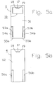
- Fgs. 5a and 5b illustrate a construction wherein the electrically-conductive ground-enlarger is in the form of stub ground-enlargers formed in the end of the PWB 4 opposite to that carrying the internal antenna 10 and the signal input terminal 17 of the antenna.
- the PWB 4 is provided with an electrically-conductive layer on both of its opposite faces, as shown at 51 in Fig. 5a and 52 in Fig. 5b .
- the face 51, shown in Fig. 5a which carries the internal antenna 10, is formed, at the opposite end from that carrying the internal antenna 10, with a pair of slots 53a, 53b, cut in the conductive layer 51 defining the ground plane.
- Each of the slots 53a, 53b is closed at one end and open at the opposite end to define two stub ground-enlargers 54a, 54b, and electrical connections 55a, 55b at the ground plane 51.
- the electrically-conductive layer 52 on the opposite face of the PWB 4 (as shown in Fig. 5b ) is formed with two interruptions 56a, 56b i.e., areas without conductors, in the ground plane 52 in alignment with the stub ground-enlargers 54a, 54b.
- the stub ground-enlargers 54a, 54b thus act similarly to the ground-enlarger 30 in Fig. 3 , to effectively enlarge the ground plane 51 of the PWB 4, but better enable tuning to enhance the operating efficiency of the antenna in the lower radio frequency band.
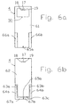
- Figs. 6a and 6b illustrate a construction similar to that of Figs. 5a and 5b , except that the stub ground-enlargers and the interruptions are reversed with respect to the opposite faces of the PWB 4.
- the etectrically-conductive layer 61 on the side of PWB 4 carrying the internal antenna 10 is formed with the interruptions 66a, 66b; whereas the opposite face of the PWB 4 carrying the electrically-conductive layer 62 is formed with the slots 63a, 63b, defining the stub ground-enlargers 64a, 64b.
- the electrical connections for exciting the stub ground-enlargers 64a, 64b are in the form of PTHs 65a, 65b, and the conductive portions 67a, 67b of layer 62 electrically connecting conductive layer 61 to the stub ground-enlargers 64a, 64b; while the slots 63a, 63b insulate the stub ground-enlargers from the electrically-conductive layer 62.
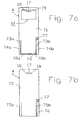
- Figs. 7a and 7b illustrate an arrangement also similar to that of Figs. 5a and 5b , respectively, but wherein the two stub ground-enlargers are of an asymmetrical construction.
- the slots 73a, 73b are cut in the electrically-conductive layer 71 of the PWB 4 in the form of two half-closed slots of different configurations so as to define two stub ground-enlargers 74a, 74b of different configurations and electrically connected to the electrically-conductive layer 71 (serving as the ground) by electrical connections 78a, 78b also of different configurations.
- Interruption 75a in the electrically-conductive layer 72 on the opposite face of the PWB 4 is of a rectangular configuration, whereas interruption 75b is of an L-shaped configuration such as to define a ground-enlarger extension 76 on face 72 ( Fig. 7b ).
- Ground-enlarger extension 76 is electrically connected by a plated-through-hole 77 (or pin, etc) to the stub ground-enlarger 74b on the opposite face of the PWB 4.
- the electrical connections 78a, 78b to the stub ground-enlargers are separated by gap 79 in the two slots 73a, 73b.
- the main PWB 4 can be separately tuned to enhance the antenna operation in two low frequency bands.
- stub ground-enlarger 74a and the ground-enlarger extension 76 shown are open ended, it is appreciated that each of them can also be grounded at its end.
- Figs. 8a and 8b illustrate a construction similar to that of Figs. 6a and 6b , except that the stub ground-enlargers are asymmetrical, and the connections of the antenna 10 to the PWB 4 are by means of two terminals rather than three terminals.
- the internal antenna 10 carried by the PWB 4 includes a signal input terminal 17, but only a ground terminal 18 on one side of the latter terminal. The location of the terminal 18 can be changed as desired.
- interruptions 86a, 86b formed in the conductive layer 81 on one side of the PWB 4, and the slots 83a, 83b, formed in the electrically-conductive layer 82 on the opposite face of the PWB are the same as the corresponding interruptions 66a, 66b and slots 63a, 63b in Figs. 6a, 6b , except that they are asymmetrical.
- the electrical connections for exciting the stub ground-enlargers 84a, 84b in the form of PTH 85a, 85b or the like, the electrical connections 87a, 87b electrically connecting conductive layer 81 to the stub ground-enlargers are asymmetrical as well.
- stub ground-enlargers could be used.
- the stub ground-enlargers could include, discrete reactive elements, such as described in U.S. Patent 5,068,670 .
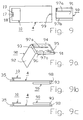
- Fig. 9 illustrates a construction wherein the electrically-conductive ground-enlarger, therein designated 90, is in the form of a plural-sided, i.e., six-sided box to be carried by the end of the PWB 4 opposite to that carrying the internal antenna 10 and the signal input terminal 17 of that ground-enlarger.
- the six sides of box ground-enlarger 90 are shown at 91 - 96, respectively, in Fig. 9a .
- Side 91 includes an electrically-conductive layer formed with an open slot 97a, and a closed slot 97b.
- Side 93 is made completely electrically-conductive, whereas the remaining sides 92, 94, 95 and 96 are electrically insulating.
- the ground-enlarger box 90 may be mounted below the PWB 4 ( Fig. 9b ) or above ( Fig. 9c ). In either case, its electrically-conductive layers (91, 93) are electrically connected to the electrically-conductive layer of the PWB 4 in any suitable manner, e.g., as by a spring-loaded conductive pin 98 passing through a plated-through-hole 99 in the PWB 4 and engaging electrically-conductive side 93.
- the purpose of the electrically-conductive layers of the ground-enlarger 90 is to effectively enlarge the ground plane of the PWB 4 so as to load the antenna 10 in the lower radio frequency band, and thereby to enhance the operating efficiency of the antenna in the lower radio frequency band.
- the ground-enlarger box 90 may therefore have a different number or arrangement of electrically-conductive layers for effectively enlarging the ground of the PWB 4.
- the slots 97a, 97b may be of different locations and/or configurations to improve the matching, and thereby to enhance the radiation of the antenna in the desired operational band. In some cases, only one slot, or no slots, may be provided.
- the antenna is an internal antenna. It will be appreciated, however, that the invention could also be implemented in mobile communication apparatus having external antennas.
- the electrically-conductive ground-enlarger, shown at 105, for effectively enlarging the ground of the PWB 103 to load the antenna 104 in a lower radio frequency band may be any of the constructions described above. It is electrically connected to the ground conductive layer 106 at the opposite end of the PWB 103 connected to the antenna by a pin 107 passing through PTHs 108, 109 in the PWB and the ground-enlarger, respectively.
- the ground-enlarger 105 may be mounted to underlie the PWB 103 as shown in Fig. 10b , to overlie it as shown in Fig. 10c , or at any angle thereto.
- Figs. 11a and 11b illustrate another implementation of the invention, in the form of a mobile telephone handset, generally designated 110, including a main housing 112 containing the main PWB 113, an external antenna 114, and a flip section 115 containing the microphone of the handset.
- the ground-enlarger provided to effectively enlarge the ground of the PWB 113 is carried by the flip section 115 as shown at 116.
- the ground-enlarger 116 is electrically connected to the ground of the PWB 113 at its end opposite to that connected to the external antenna 114 in any suitable manner, e.g., by an electrically-conductive flexible 117 in the pivoted coupling of the flip section 115 to the housing 112.
- the housing has two sections movable relative to each other, (e.g., relatively slidable sections), in which the PWB, communication circuitry and signal terminal are in one section.
- the invention may also be implemented in those constructions, e.g., by including the electrically-conductive ground-enlarger in the other section.
Landscapes
- Engineering & Computer Science (AREA)
- Computer Networks & Wireless Communication (AREA)
- Support Of Aerials (AREA)
- Aerials With Secondary Devices (AREA)
- Transceivers (AREA)
- Variable-Direction Aerials And Aerial Arrays (AREA)
- Waveguide Aerials (AREA)
- Telephone Set Structure (AREA)
- Mobile Radio Communication Systems (AREA)
- Details Of Aerials (AREA)
Claims (31)
- Mobiles Kommunikationsgerät, umfassend:ein Gehäuse (2), das eine Kommunikationsschaltung (6) und eine mit einem Signalanschluss (7) für eine Antenne gebildete Leiterplatte PWB (printed wire board) (4) und eine elektrisch leitende Masseplatte für die Kommunikationsschaltung einschließt;wobei die Masseplatte und die Kommunikationsschaltung auf der PWB getragen werden;
und eine Antenne (10), die durch das Gehäuse getragen wird und mit dem Signalanschluss der Kommunikationsschaltung (6) an einem Ende der PWB (4) elektrisch verbunden ist, wobei die Antenne derart gestaltet ist, dass sie auf mindestens einem Funkfrequenzband arbeitet, wobei die Antenne im Wesentlichen an dem einen Ende der PWB lokalisiert ist;
dadurch gekennzeichnet, dass das Gerät des Weiteren eine durch die PWB getragene elektrisch leitende Massenerweiterung (30 usw.) aufweist und mit der elektrisch leitenden Masseplatte der PWB derart verbunden ist, dass die elektrisch leitende Massenerweiterung mit der Masseplatte der Kommunikationsschaltung am gegenüberliegenden Ende der PWB verbunden ist und am gegenüberliegenden Ende der PWB lokalisiert ist und die Masseplatte der PWB wirksam vergrößert, um die Antenne in das Funkfrequenzband zu laden und dadurch die Betriebseffizienz der Antenne, insbesondere im unteren Teil des Funkfrequenzbands zu erhöhen und/oder das Funkfrequenzband zu erweitern. - Gerät nach Anspruch 1, wobei die Massenerweiterung auf einer Platte (30) getragen wird, die von der PWB (4, Fig.3) getrennt ist und mit der Masseplatte der Kommunikationsschaltung am gegenüberliegenden Ende der PWB elektrisch verbunden ist.
- Gerät nach Anspruch 2, wobei die Massenerweiterungsplatte (30) an der PWB (4) befestigt ist und unter dem gegenüberliegenden Ende der PWB (Fig. 3b) liegt.
- Gerät nach Anspruch 2, wobei die Massenerweiterungsplatte (40, Fig. 4) an der PWB (4) befestigt ist und über dem gegenüberliegenden Ende der PWB (Fig. 3a) liegt.
- Gerät nach Anspruch 2, wobei die Massenerweiterungsplatte (40, Fig. 4) mit der PWB (4) am gegenüberliegenden Ende davon integral gebildet und in Bezug auf das gegenüberliegende Ende der PWB gefaltet ist.
- Gerät nach Anspruch 1, wobei die Masseplatte (61, Fig. 6a) der Kommunikationsschaltung (6) auf einer Schicht der PWB (4) getragen wird und die Massenerweiterung (64a, 64b, Fig. 6b) auf einer anderen Schicht der PWB getragen wird.
- Gerät nach Anspruch 1, wobei der Signalanschluss (17) der Kommunikationsschaltung (6) auf einer Schicht der PWB (4) an einem Ende davon liegt und die Massenerweiterung (64a, 64b, Fig. 6b) an einer anderen Schicht der PWB am gegenüberliegenden Ende davon getragen wird.
- Gerät nach Anspruch 1, wobei die Massenerweiterung mindestens eine durch die PWB (4) getragene Stichleitungs-Massenerweiterung (54a, 54b; usw.) einschließt.
- Gerät nach Anspruch 1, wobei der Signalanschluss (17) der Kommunikationsschaltung an einem Ende der PWB liegt und die Massenerweiterung mindestens eine Stichleitungs-Massenerweiterung (54a, 54b; usw.) am gegenüberliegenden Ende der PWB einschließt.
- Gerät nach Anspruch 9, wobei die Massenerweiterung ein Paar in der elektrisch leitenden Masseplatte (51; usw.) der PWB (4) am gegenüberliegenden Ende der PWB gebildete Stichleitungs-Massenerweiterungen (54a, 54b; usw.) einschließt.
- Gerät nach Anspruch 10, wobei das gegenüberliegende Ende der PWB (4) eine elektrisch leitende Masseplatte an einer Schicht (51; usw.) der PWB einschließt, wobei die Stichleitungs-Massenerweiterung (54a, 54b; usw.) durch in der elektrisch leitenden Masseplatte an der einen Schicht gebildete Schlitze (53a, 53b; usw.) definiert sind.
- Gerät nach Anspruch 11, wobei die PWB (4) eine elektrisch leitende Masseplatte (52) an einer zweiten Schicht der PWB einschließt, wobei die zweite Schicht mit Unterbrechungen (56a, 56b) in der elektrisch leitenden Masseplatte gebildet ist, wobei die Unterbrechungen mit den Stichleitungs-Massenerweiterungen (54a, 54b) in der einen Schicht ausgerichtet sind.
- Gerät nach Anspruch 11, wobei die Stichleitungs-Massenerweiterungen (64a, 64b) elektrisch leitende Teile an einer anderen Schicht (62) der PWB einschließen, mit denen die Stichleitungs-Massenerweiterungen elektrisch verbunden sind (65a, 65b).
- Gerät nach Anspruch 1, wobei die elektrisch leitende Massenerweiterung in einer Box (90) mit einer Mehrzahl an Seiten, die über einem Ende der PWB liegen, eingeschlossen ist, wobei mindestens eine (91) der Seiten der Box elektrisch leitend ist und als die mit der Masseplatte der PWB elektrisch verbundene Massenerweiterung dient.
- Gerät nach Anspruch 14, wobei eine Mehrzahl (91, 93) der Seiten der elektrisch leitenden Massenerweiterungsbox elektrisch leitend ist und als die mit der Masseplatte der PWB elektrisch verbundene Massenerweiterung dient.
- Gerät nach Anspruch 14, wobei die mindestens eine elektrisch leitende Seite (91) der Massenerweiterungsbox mit mindestens einem Schlitz (97a, 97b) gebildet ist, um die durch die Massenerweiterungsbox erzeugte Last zu modifizieren.
- Gerät nach Anspruch 1, wobei die Antenne (10) eine Innenantenne in dem Gehäuse (2) ist und mit der PWB (4) in dem Gehäuse (Fig. 1-9) elektrisch verbunden ist.
- Gerät nach Anspruch 1, wobei die Antenne eine Außenantenne (104; 114) ist, die durch das Gehäuse extern davon getragen wird und mit der PWB in dem Gehäuse elektrisch verbunden ist.
- Gerät nach Anspruch 1, wobei die Antenne zusätzlich zu ihrer Verbindung mit dem Signalanschluss der PWB mit der Masseplatte der PWB elektrisch verbunden ist.
- Gerät nach Anspruch 1, wobei das mobile Kommunikationsgerät ein Mobiltelefonhandapparat (Fig. 11a, 11b) ist und ein Gehäuse mit zwei in Bezug zueinander bewegbaren Abschnitten (112, 115) einschließt, wobei einer (112) der Gehäuseabschnitte die PWB, die Kommunikationsschaltung und den Signalanschluss für eine Antenne einschließt, der andere (115) der Gehäuseabschnitte die elektrisch leitende Massenerweiterung (116) einschließt.
- Gerät nach Anspruch 20, wobei der andere Gehäuseabschnitt in Bezug auf den einen Gehäuseabschnitt drehbar (bei 117) ist.
- Verfahren zum Erhöhen der Betriebseffizienz eines mobilen Kommunikationsgeräts in mindestens-einem Funkfrequenzband oder zum Erweitern seines Funkfrequenzbands, wobei das Gerät ein Gehäuse (2), einschließend eine Kommunikationsschaltung (6) und eine mit einem Signalanschluss (7) für eine Antenne (10) gebildete Leiterplatte PWB (4), und eine elektrisch leitende Masseplatte für die Kommunikationsschaltung umfasst,
wobei die Masseplatte und die Kommunikationsschaltung auf der PWB getragen werden und eine durch das Gehäuse getragene und elektrisch mit dem Signalanschluss (7) der Kommunikationsschaltung (6) an einem Ende der PWB (4) verbundene Antenne (10), wobei die Antenne im Wesentlichen am einen Ende der PWB lokalisiert ist;
dadurch gekennzeichnet, dass die Betriebseffizienz der Antenne insbesondere im unteren Teil des Funkfrequenzbands erhöht ist oder ihr Funkfrequenzband erweitert ist durch Verbinden einer elektrisch leitenden Massenerweiterung (30, usw.) mit der elektrisch leitenden Masseplatte der Kommunikationsschaltung am gegenüberliegenden Ende der PWB, sodass die elektrisch leitende Massenerweiterung am gegenüberliegenden Ende der PWB lokalisiert ist und die Masse der PWB vergrößert, um die Antenne in das Funkfrequenzband zu laden. - Verfahren nach Anspruch 22, wobei die Massenerweiterung auf einer separaten Platte (30) der PWB (4, Fig. 3) getragen wird und mit dem gegenüberliegenden Ende der PWB elektrisch verbunden ist.
- Verfahren nach Anspruch 22, wobei die Masseplatte (61, Fig. 6a) der Kommunikationsschaltung (6) auf einer Schicht der PWB (4) getragen wird und die Massenerweiterung (64a, 64b, Fig. 6b) auf einer anderen Seite der PWB getragen wird.
- Verfahren nach Anspruch 22, wobei der Signalanschluss (17) der Kommunikationsschaltung (6) auf einer Schicht der PWB (4) an einem Ende davon ist und die Massenerweiterung (64b, Fig. 6b) auf einer anderen Schicht der PWB an einem gegenüberliegenden Ende davon getragen wird.
- Verfahren nach Anspruch 22, wobei die Massenerweiterung mindestens eine durch die PWB (4) getragene Stichleitungs-Massenerweiterung (54a, 54b, usw.) einschließt.
- Verfahren nach Anspruch 22, wobei die Antenne (10) eine Innenantenne im Gehäuse (2) ist und mit der PWB (4) im Gehäuse (Fig. 1-9) elektrisch verbunden ist.
- Verfahren nach Anspruch 22, wobei die Antenne (114) eine durch das Gehäuse extern davon getragene Außenantenne ist und mit der PWB im Gehäuse elektrisch verbunden ist.
- Verfahren nach Anspruch 22, wobei die Antenne zusätzlich zu ihrer Verbindung mit dem Signalanschluss der PWB mit der Masseplatte der PWB elektrisch verbunden ist.
- Verfahren nach Anspruch 22, wobei das mobile Kommunikationsgerät ein Mobiltelefonhandapparat (Fig. 11a, 11b) ist und ein Gehäuse mit zwei Abschnitten (112, 115) einschließt, die in Bezug zueinander bewegbar sind, wobei einer (112) der Gehäuseabschnitte die PWB, die Kommunikationsschaltung und den Signalanschluss für eine Antenne einschließt, der andere (115) der Gehäuseabschnitte die elektrisch leitende Massenerweiterung einschließt.
- Verfahren nach Anspruch 22, wobei die elektrisch leitende Massenerweiterung mit Schlitzen (53a, usw.) gebildet ist, um die dadurch erzeugte Belastung zu modifizieren.
Applications Claiming Priority (3)
| Application Number | Priority Date | Filing Date | Title |
|---|---|---|---|
| US22812300P | 2000-08-28 | 2000-08-28 | |
| US228123P | 2000-08-28 | ||
| PCT/IL2001/000767 WO2002019671A1 (en) | 2000-08-28 | 2001-08-16 | Apparatus and method for enhancing low-frequency operation of mobile communication antennas |
Publications (3)
| Publication Number | Publication Date |
|---|---|
| EP1323281A1 EP1323281A1 (de) | 2003-07-02 |
| EP1323281A4 EP1323281A4 (de) | 2005-03-30 |
| EP1323281B1 true EP1323281B1 (de) | 2008-06-25 |
Family
ID=22855897
Family Applications (1)
| Application Number | Title | Priority Date | Filing Date |
|---|---|---|---|
| EP01958358A Expired - Lifetime EP1323281B1 (de) | 2000-08-28 | 2001-08-16 | Vorrichtung und verfahren zur verbesserung des niederfrequenten betriebs von mobilkommunikationsantennen |
Country Status (12)
| Country | Link |
|---|---|
| US (1) | US6940460B2 (de) |
| EP (1) | EP1323281B1 (de) |
| JP (1) | JP4162993B2 (de) |
| KR (1) | KR100675264B1 (de) |
| CN (1) | CN100581179C (de) |
| AT (1) | ATE399431T1 (de) |
| AU (2) | AU2001280076B2 (de) |
| CA (1) | CA2420959C (de) |
| DE (1) | DE60134560D1 (de) |
| ES (1) | ES2309083T3 (de) |
| TW (1) | TW504858B (de) |
| WO (1) | WO2002019671A1 (de) |
Families Citing this family (60)
| Publication number | Priority date | Publication date | Assignee | Title |
|---|---|---|---|---|
| US6648821B2 (en) * | 2000-01-21 | 2003-11-18 | Medtronic Minimed, Inc. | Microprocessor controlled ambulatory medical apparatus with hand held communication device |
| BR0117125A (pt) | 2001-09-13 | 2004-09-28 | Fractus Sa | Polarização horizontal para um dispositivo de antena e dispositivo de antena |
| WO2004001895A1 (ja) * | 2002-06-25 | 2003-12-31 | Matsushita Electric Industrial Co., Ltd. | 携帯無線機用アンテナ |
| JP2004104419A (ja) * | 2002-09-09 | 2004-04-02 | Hitachi Cable Ltd | 携帯無線機用アンテナ |
| FI114836B (fi) * | 2002-09-19 | 2004-12-31 | Filtronic Lk Oy | Sisäinen antenni |
| US20040233172A1 (en) * | 2003-01-31 | 2004-11-25 | Gerhard Schneider | Membrane antenna assembly for a wireless device |
| JP4021814B2 (ja) * | 2003-06-30 | 2007-12-12 | 本田技研工業株式会社 | 車載アンテナ |
| DE602004012377T2 (de) * | 2003-09-18 | 2009-03-12 | Sony Ericsson Mobile Communications Japan, Inc. | Endgerät für eine mobile Kommunikation |
| US7203549B2 (en) * | 2003-10-02 | 2007-04-10 | Medtronic, Inc. | Medical device programmer with internal antenna and display |
| US7272445B2 (en) * | 2003-10-02 | 2007-09-18 | Medtronic, Inc. | Medical device programmer with faceplate |
| US7729766B2 (en) * | 2003-10-02 | 2010-06-01 | Medtronic, Inc. | Circuit board construction for handheld programmer |
| US7263406B2 (en) | 2003-10-02 | 2007-08-28 | Medtronic, Inc. | Medical device programmer with selective disablement of display during telemetry |
| US7356369B2 (en) * | 2003-10-02 | 2008-04-08 | Medtronic, Inc. | Z-axis assembly of medical device programmer |
| US7561921B2 (en) * | 2003-10-02 | 2009-07-14 | Medtronic, Inc. | Neurostimulator programmer with internal antenna |
| US7991479B2 (en) * | 2003-10-02 | 2011-08-02 | Medtronic, Inc. | Neurostimulator programmer with clothing attachable antenna |
| US20050075685A1 (en) * | 2003-10-02 | 2005-04-07 | Forsberg John W. | Medical device programmer with infrared communication |
| US7187959B2 (en) * | 2003-11-25 | 2007-03-06 | Motorola, Inc. | Antenna structure for devices with conductive chassis |
| JP4444021B2 (ja) | 2004-06-29 | 2010-03-31 | パナソニック株式会社 | 折畳式携帯無線機 |
| CN1977419B (zh) * | 2004-09-28 | 2011-08-24 | 松下电器产业株式会社 | 无线电设备的天线装置和便携式无线电设备 |
| KR101176027B1 (ko) * | 2004-10-19 | 2012-08-24 | 가부시키가이샤 한도오따이 에네루기 켄큐쇼 | 안테나를 구비한 반도체장치 및 그 제조 방법 |
| KR100681759B1 (ko) * | 2004-11-24 | 2007-02-15 | 삼성전자주식회사 | 안테나 성능 개선을 위한 도전체를 갖는 휴대용 무선단말기 |
| JP4966662B2 (ja) * | 2005-04-13 | 2012-07-04 | パナソニック株式会社 | 携帯無線機 |
| TWI257739B (en) * | 2005-05-26 | 2006-07-01 | Wistron Neweb Corp | Mobile communication device |
| US7317421B2 (en) * | 2005-08-24 | 2008-01-08 | Accton Technology Corporation | Antenna module with an enhanced angular coverage |
| KR20080046168A (ko) * | 2005-09-07 | 2008-05-26 | 톰슨 라이센싱 | 콤팩트 멀티밴드 안테나 |
| US7903034B2 (en) | 2005-09-19 | 2011-03-08 | Fractus, S.A. | Antenna set, portable wireless device, and use of a conductive element for tuning the ground-plane of the antenna set |
| SE0502225L (sv) * | 2005-10-10 | 2006-10-17 | Amc Centurion Ab | Antennanordning |
| KR100683868B1 (ko) * | 2005-12-05 | 2007-02-15 | 삼성전자주식회사 | 슬라이드형 이동통신 단말장치에 적용되는 안테나 |
| US7479927B2 (en) * | 2005-12-30 | 2009-01-20 | Motorola, Inc. | Radio frequency antenna system |
| US7755547B2 (en) * | 2006-06-30 | 2010-07-13 | Nokia Corporation | Mechanically tunable antenna for communication devices |
| KR100819281B1 (ko) * | 2006-10-30 | 2008-04-02 | 삼성전자주식회사 | 휴대용 단말기의 배터리 커버 접지 장치 |
| EP2160796B1 (de) * | 2007-06-22 | 2017-04-05 | Nokia Technologies Oy | Antennenanordnung |
| WO2009037523A2 (en) * | 2007-09-20 | 2009-03-26 | Nokia Corporation | An antenna arrangement, a method for manufacturing an antenna arrangement and a printed wiring board for use in an antenna arrangement |
| TWI352458B (en) * | 2008-04-09 | 2011-11-11 | Univ Nat Taiwan | Antenna |
| KR101044994B1 (ko) * | 2008-06-20 | 2011-06-29 | 삼성전자주식회사 | 휴대 단말기의 안테나 장치 |
| EP2151890A1 (de) * | 2008-08-07 | 2010-02-10 | Laird Technologies AB | Antennenanordnung für eine Funkkommunikationsvorrichtung und tragbare Funkkommunikationsvorrichtung mit einer solchen Antennenanordnung |
| TWI358852B (en) | 2008-09-03 | 2012-02-21 | Htc Corp | Handset device |
| TWI411159B (zh) * | 2009-03-11 | 2013-10-01 | Acer Inc | 一種具有降低接地面效應之行動通訊天線 |
| TWI411163B (zh) * | 2009-06-06 | 2013-10-01 | Acer Inc | 一種行動通訊裝置 |
| CN101610310B (zh) * | 2009-07-07 | 2013-05-15 | 惠州Tcl移动通信有限公司 | 一种移动通讯终端 |
| KR20110078048A (ko) * | 2009-12-30 | 2011-07-07 | 엘지전자 주식회사 | 휴대 단말기 |
| US8746577B2 (en) * | 2010-09-20 | 2014-06-10 | The Board Of Trustees Of The University Of Illinois | Placement insensitive antenna for RFID, sensing, and/or communication systems |
| US8514138B2 (en) * | 2011-01-12 | 2013-08-20 | Mediatek Inc. | Meander slot antenna structure and antenna module utilizing the same |
| KR101801186B1 (ko) * | 2011-02-25 | 2017-11-24 | 엘지전자 주식회사 | 이동 단말기 |
| CN102683828B (zh) * | 2011-03-09 | 2015-02-25 | 光宝电子(广州)有限公司 | 具有袖状扼流结构的天线装置 |
| CN103165983A (zh) | 2011-12-16 | 2013-06-19 | 华为技术有限公司 | 一种天线装置、设备及信号发射装置 |
| US8902109B2 (en) * | 2012-02-05 | 2014-12-02 | Auden Techno Corp. | Communication device |
| CN102664303B (zh) * | 2012-04-27 | 2016-01-20 | 深圳光启创新技术有限公司 | 具有内置型天线的电子装置 |
| CN102821565A (zh) * | 2012-07-31 | 2012-12-12 | 深圳光启创新技术有限公司 | 一种电子设备及其壳体 |
| CN102821570A (zh) * | 2012-07-31 | 2012-12-12 | 深圳光启创新技术有限公司 | 电子设备及其壳体 |
| TWI527307B (zh) | 2013-05-29 | 2016-03-21 | 智易科技股份有限公司 | 天線結構 |
| TWI599105B (zh) * | 2015-07-31 | 2017-09-11 | 宏碁股份有限公司 | 行動通訊裝置 |
| US10734713B2 (en) | 2016-04-27 | 2020-08-04 | Fractus Antennas, S.L. | Ground plane booster antenna technology for wearable devices |
| KR102137492B1 (ko) * | 2016-11-28 | 2020-07-27 | 한국전자통신연구원 | 통신 장치 및 이를 포함하는 통신 시스템 |
| KR20190120349A (ko) * | 2017-03-06 | 2019-10-23 | 스냅 인코포레이티드 | 웨어러블 디바이스 안테나 시스템 |
| KR101966709B1 (ko) * | 2017-03-08 | 2019-04-09 | 한국철도기술연구원 | 비콘 안테나 장치 |
| SE541063C2 (en) * | 2017-10-30 | 2019-03-26 | Smarteq Wireless Ab | Ground plane independent antenna |
| CN108400430B (zh) * | 2018-02-06 | 2021-08-17 | 中兴通讯股份有限公司 | 一种天线装置及终端 |
| JP7152190B2 (ja) * | 2018-05-28 | 2022-10-12 | 矢崎総業株式会社 | 検出機器及び検出システム |
| CN112968273B (zh) * | 2021-02-03 | 2024-05-17 | 惠州Tcl移动通信有限公司 | 一种天线结构以及终端设备 |
Family Cites Families (36)
| Publication number | Priority date | Publication date | Assignee | Title |
|---|---|---|---|---|
| US4471493A (en) * | 1982-12-16 | 1984-09-11 | Gte Automatic Electric Inc. | Wireless telephone extension unit with self-contained dipole antenna |
| IL82331A (en) * | 1987-04-26 | 1991-04-15 | M W A Ltd | Microstrip and stripline antenna |
| RU1838850C (ru) * | 1988-11-02 | 1993-08-30 | Моторола, Инк. | Выдвижна антенна система дл портативного приемопередатчика |
| JPH0496520A (ja) * | 1990-08-13 | 1992-03-27 | Sharp Corp | データ送信装置 |
| GB9102935D0 (en) * | 1991-02-12 | 1991-03-27 | Shaye Communications Ltd | Improvements in and relating to antennae |
| US5262792A (en) * | 1991-09-11 | 1993-11-16 | Harada Kogyo Kabushiki Kaisha | Shortened non-grounded type ultrashort-wave antenna |
| GB9309368D0 (en) * | 1993-05-06 | 1993-06-16 | Ncr Int Inc | Antenna apparatus |
| NL9302192A (nl) * | 1993-07-09 | 1995-02-01 | Ericsson Business Mobile Netwo | Draadloze telefoon. |
| US5539414A (en) * | 1993-09-02 | 1996-07-23 | Inmarsat | Folded dipole microstrip antenna |
| CA2152860A1 (en) * | 1994-07-15 | 1996-01-16 | Argyrios A. Chatzipetros | Antenna for communication device |
| US5561436A (en) * | 1994-07-21 | 1996-10-01 | Motorola, Inc. | Method and apparatus for multi-position antenna |
| US6452553B1 (en) * | 1995-08-09 | 2002-09-17 | Fractal Antenna Systems, Inc. | Fractal antennas and fractal resonators |
| JP3130461B2 (ja) * | 1995-11-13 | 2001-01-31 | 株式会社ケンウッド | 携帯用無線機 |
| SE507077C2 (sv) * | 1996-05-17 | 1998-03-23 | Allgon Ab | Antennanordning för en portabel radiokommunikationsanordning |
| US6072434A (en) * | 1997-02-04 | 2000-06-06 | Lucent Technologies Inc. | Aperture-coupled planar inverted-F antenna |
| US6031503A (en) * | 1997-02-20 | 2000-02-29 | Raytheon Company | Polarization diverse antenna for portable communication devices |
| FI113212B (fi) * | 1997-07-08 | 2004-03-15 | Nokia Corp | Usean taajuusalueen kaksoisresonanssiantennirakenne |
| SE511131C2 (sv) * | 1997-11-06 | 1999-08-09 | Ericsson Telefon Ab L M | Portabel elektronisk kommunikationsanordning med flerbandigt antennsystem |
| SE511068C2 (sv) * | 1997-11-06 | 1999-08-02 | Ericsson Telefon Ab L M | Portabel elektronisk kommunikationsanordning med dubbelbandigt antennsystem |
| FR2772517B1 (fr) * | 1997-12-11 | 2000-01-07 | Alsthom Cge Alcatel | Antenne multifrequence realisee selon la technique des microrubans et dispositif incluant cette antenne |
| EP0929115A1 (de) * | 1998-01-09 | 1999-07-14 | Nokia Mobile Phones Ltd. | Antenne für mobiles Kommunikationsgerät |
| US5929813A (en) * | 1998-01-09 | 1999-07-27 | Nokia Mobile Phones Limited | Antenna for mobile communications device |
| US5945954A (en) * | 1998-01-16 | 1999-08-31 | Rangestar International Corporation | Antenna assembly for telecommunication devices |
| JP3340374B2 (ja) * | 1998-01-27 | 2002-11-05 | 株式会社東芝 | 多周波アンテナ |
| JP3252786B2 (ja) * | 1998-02-24 | 2002-02-04 | 株式会社村田製作所 | アンテナ装置およびそれを用いた無線装置 |
| GB2335081B (en) * | 1998-03-05 | 2002-04-03 | Nec Technologies | Antenna for mobile telephones |
| FR2778272B1 (fr) * | 1998-04-30 | 2000-09-08 | Alsthom Cge Alcatel | Dispositif de radiocommunication et antenne bifrequence realisee selon la technique des microrubans |
| US6016126A (en) * | 1998-05-29 | 2000-01-18 | Ericsson Inc. | Non-protruding dual-band antenna for communications device |
| JP4075154B2 (ja) * | 1998-09-21 | 2008-04-16 | ソニー株式会社 | アンテナ装置及び携帯無線装置 |
| US6049314A (en) * | 1998-11-17 | 2000-04-11 | Xertex Technologies, Inc. | Wide band antenna having unitary radiator/ground plane |
| JP3351363B2 (ja) * | 1998-11-17 | 2002-11-25 | 株式会社村田製作所 | 表面実装型アンテナおよびそれを用いた通信装置 |
| FI105421B (fi) * | 1999-01-05 | 2000-08-15 | Filtronic Lk Oy | Tasomainen kahden taajuuden antenni ja tasoantennilla varustettu radiolaite |
| FI113588B (fi) * | 1999-05-10 | 2004-05-14 | Nokia Corp | Antennirakenne |
| US6373442B1 (en) * | 1999-05-28 | 2002-04-16 | David L. Thomas | Antenna for a parking meter |
| US6329949B1 (en) * | 2000-03-09 | 2001-12-11 | Avaya Technology Corp. | Transceiver stacked assembly |
| US6421016B1 (en) * | 2000-10-23 | 2002-07-16 | Motorola, Inc. | Antenna system with channeled RF currents |
-
2001
- 2001-08-16 AU AU2001280076A patent/AU2001280076B2/en not_active Ceased
- 2001-08-16 AT AT01958358T patent/ATE399431T1/de not_active IP Right Cessation
- 2001-08-16 ES ES01958358T patent/ES2309083T3/es not_active Expired - Lifetime
- 2001-08-16 CA CA002420959A patent/CA2420959C/en not_active Expired - Fee Related
- 2001-08-16 US US10/362,219 patent/US6940460B2/en not_active Expired - Fee Related
- 2001-08-16 KR KR1020037003015A patent/KR100675264B1/ko not_active Expired - Fee Related
- 2001-08-16 WO PCT/IL2001/000767 patent/WO2002019671A1/en not_active Ceased
- 2001-08-16 JP JP2002523839A patent/JP4162993B2/ja not_active Expired - Fee Related
- 2001-08-16 CN CN01818128A patent/CN100581179C/zh not_active Expired - Fee Related
- 2001-08-16 DE DE60134560T patent/DE60134560D1/de not_active Expired - Lifetime
- 2001-08-16 AU AU8007601A patent/AU8007601A/xx active Pending
- 2001-08-16 EP EP01958358A patent/EP1323281B1/de not_active Expired - Lifetime
- 2001-08-21 TW TW090120503A patent/TW504858B/zh not_active IP Right Cessation
Also Published As
| Publication number | Publication date |
|---|---|
| KR100675264B1 (ko) | 2007-01-29 |
| AU2001280076B2 (en) | 2007-04-05 |
| WO2002019671A1 (en) | 2002-03-07 |
| WO2002019671A8 (en) | 2002-05-16 |
| AU8007601A (en) | 2002-03-13 |
| ATE399431T1 (de) | 2008-07-15 |
| US20040125029A1 (en) | 2004-07-01 |
| CN100581179C (zh) | 2010-01-13 |
| EP1323281A4 (de) | 2005-03-30 |
| DE60134560D1 (de) | 2008-08-07 |
| US6940460B2 (en) | 2005-09-06 |
| EP1323281A1 (de) | 2003-07-02 |
| JP2004522332A (ja) | 2004-07-22 |
| JP4162993B2 (ja) | 2008-10-08 |
| HK1055367A1 (en) | 2004-01-02 |
| CA2420959C (en) | 2009-11-03 |
| ES2309083T3 (es) | 2008-12-16 |
| TW504858B (en) | 2002-10-01 |
| CN1600016A (zh) | 2005-03-23 |
| CA2420959A1 (en) | 2002-03-07 |
| KR20030032001A (ko) | 2003-04-23 |
Similar Documents
| Publication | Publication Date | Title |
|---|---|---|
| EP1323281B1 (de) | Vorrichtung und verfahren zur verbesserung des niederfrequenten betriebs von mobilkommunikationsantennen | |
| AU2001280076A1 (en) | Apparatus and method for enhancing low-frequency operation of mobile communication antennas | |
| EP1307947B1 (de) | Interne antennen für mobilkommunikationsgeräte | |
| US7439916B2 (en) | Antenna for mobile communication terminals | |
| US6759991B2 (en) | Antenna arrangement | |
| US6747601B2 (en) | Antenna arrangement | |
| Chen et al. | PIFA with a meandered and folded patch for the dual-band mobile phone application | |
| AU2001269413A1 (en) | Internal antennas for mobile communication devices | |
| US6795028B2 (en) | Wideband compact planar inverted-F antenna | |
| JPH11251825A (ja) | 多周波共振型逆f型アンテナ | |
| ZA200300242B (en) | Internal antennas for mobile communication devices. | |
| HK1055367B (en) | Apparatus and method for enhancing low-frequency operation of mobile communication antennas | |
| IL154645A (en) | Apparatus and method for enhancing low-frequency operation of mobile communication antennas | |
| US7149540B2 (en) | Antenna |
Legal Events
| Date | Code | Title | Description |
|---|---|---|---|
| PUAI | Public reference made under article 153(3) epc to a published international application that has entered the european phase |
Free format text: ORIGINAL CODE: 0009012 |
|
| 17P | Request for examination filed |
Effective date: 20030314 |
|
| AK | Designated contracting states |
Designated state(s): AT BE CH CY DE DK ES FI FR GB GR IE IT LI LU MC NL PT SE TR |
|
| AX | Request for extension of the european patent |
Extension state: AL LT LV MK RO SI |
|
| A4 | Supplementary search report drawn up and despatched |
Effective date: 20050211 |
|
| RIC1 | Information provided on ipc code assigned before grant |
Ipc: 7H 01Q 1/48 B Ipc: 7H 04B 1/08 B Ipc: 7H 01Q 1/24 B Ipc: 7H 04B 1/034 B Ipc: 7H 04B 7/00 B Ipc: 7H 04B 1/38 B Ipc: 7H 01Q 9/04 B Ipc: 7H 04M 1/00 A |
|
| GRAP | Despatch of communication of intention to grant a patent |
Free format text: ORIGINAL CODE: EPIDOSNIGR1 |
|
| GRAS | Grant fee paid |
Free format text: ORIGINAL CODE: EPIDOSNIGR3 |
|
| GRAA | (expected) grant |
Free format text: ORIGINAL CODE: 0009210 |
|
| AK | Designated contracting states |
Kind code of ref document: B1 Designated state(s): AT BE CH CY DE DK ES FI FR GB GR IE IT LI LU MC NL PT SE TR |
|
| AX | Request for extension of the european patent |
Extension state: AL LT LV MK RO SI |
|
| REG | Reference to a national code |
Ref country code: GB Ref legal event code: FG4D |
|
| REG | Reference to a national code |
Ref country code: CH Ref legal event code: EP |
|
| REF | Corresponds to: |
Ref document number: 60134560 Country of ref document: DE Date of ref document: 20080807 Kind code of ref document: P |
|
| REG | Reference to a national code |
Ref country code: IE Ref legal event code: FG4D |
|
| PG25 | Lapsed in a contracting state [announced via postgrant information from national office to epo] |
Ref country code: AT Free format text: LAPSE BECAUSE OF FAILURE TO SUBMIT A TRANSLATION OF THE DESCRIPTION OR TO PAY THE FEE WITHIN THE PRESCRIBED TIME-LIMIT Effective date: 20080625 |
|
| REG | Reference to a national code |
Ref country code: ES Ref legal event code: FG2A Ref document number: 2309083 Country of ref document: ES Kind code of ref document: T3 |
|
| NLR4 | Nl: receipt of corrected translation in the netherlands language at the initiative of the proprietor of the patent | ||
| REG | Reference to a national code |
Ref country code: HK Ref legal event code: GR Ref document number: 1055367 Country of ref document: HK |
|
| PG25 | Lapsed in a contracting state [announced via postgrant information from national office to epo] |
Ref country code: PT Free format text: LAPSE BECAUSE OF FAILURE TO SUBMIT A TRANSLATION OF THE DESCRIPTION OR TO PAY THE FEE WITHIN THE PRESCRIBED TIME-LIMIT Effective date: 20081125 Ref country code: SE Free format text: LAPSE BECAUSE OF FAILURE TO SUBMIT A TRANSLATION OF THE DESCRIPTION OR TO PAY THE FEE WITHIN THE PRESCRIBED TIME-LIMIT Effective date: 20080925 |
|
| PG25 | Lapsed in a contracting state [announced via postgrant information from national office to epo] |
Ref country code: BE Free format text: LAPSE BECAUSE OF FAILURE TO SUBMIT A TRANSLATION OF THE DESCRIPTION OR TO PAY THE FEE WITHIN THE PRESCRIBED TIME-LIMIT Effective date: 20080625 |
|
| PG25 | Lapsed in a contracting state [announced via postgrant information from national office to epo] |
Ref country code: MC Free format text: LAPSE BECAUSE OF NON-PAYMENT OF DUE FEES Effective date: 20080831 |
|
| PG25 | Lapsed in a contracting state [announced via postgrant information from national office to epo] |
Ref country code: DK Free format text: LAPSE BECAUSE OF FAILURE TO SUBMIT A TRANSLATION OF THE DESCRIPTION OR TO PAY THE FEE WITHIN THE PRESCRIBED TIME-LIMIT Effective date: 20080625 |
|
| PLBE | No opposition filed within time limit |
Free format text: ORIGINAL CODE: 0009261 |
|
| STAA | Information on the status of an ep patent application or granted ep patent |
Free format text: STATUS: NO OPPOSITION FILED WITHIN TIME LIMIT |
|
| REG | Reference to a national code |
Ref country code: IE Ref legal event code: MM4A |
|
| 26N | No opposition filed |
Effective date: 20090326 |
|
| PG25 | Lapsed in a contracting state [announced via postgrant information from national office to epo] |
Ref country code: IE Free format text: LAPSE BECAUSE OF NON-PAYMENT OF DUE FEES Effective date: 20080816 |
|
| PG25 | Lapsed in a contracting state [announced via postgrant information from national office to epo] |
Ref country code: CY Free format text: LAPSE BECAUSE OF FAILURE TO SUBMIT A TRANSLATION OF THE DESCRIPTION OR TO PAY THE FEE WITHIN THE PRESCRIBED TIME-LIMIT Effective date: 20080625 Ref country code: LU Free format text: LAPSE BECAUSE OF NON-PAYMENT OF DUE FEES Effective date: 20080816 |
|
| PG25 | Lapsed in a contracting state [announced via postgrant information from national office to epo] |
Ref country code: TR Free format text: LAPSE BECAUSE OF FAILURE TO SUBMIT A TRANSLATION OF THE DESCRIPTION OR TO PAY THE FEE WITHIN THE PRESCRIBED TIME-LIMIT Effective date: 20080625 |
|
| PG25 | Lapsed in a contracting state [announced via postgrant information from national office to epo] |
Ref country code: GR Free format text: LAPSE BECAUSE OF FAILURE TO SUBMIT A TRANSLATION OF THE DESCRIPTION OR TO PAY THE FEE WITHIN THE PRESCRIBED TIME-LIMIT Effective date: 20080926 |
|
| PGFP | Annual fee paid to national office [announced via postgrant information from national office to epo] |
Ref country code: CH Payment date: 20100824 Year of fee payment: 10 Ref country code: ES Payment date: 20100825 Year of fee payment: 10 Ref country code: NL Payment date: 20100823 Year of fee payment: 10 |
|
| PGFP | Annual fee paid to national office [announced via postgrant information from national office to epo] |
Ref country code: FI Payment date: 20100823 Year of fee payment: 10 Ref country code: IT Payment date: 20100824 Year of fee payment: 10 Ref country code: FR Payment date: 20100901 Year of fee payment: 10 Ref country code: DE Payment date: 20100823 Year of fee payment: 10 |
|
| PGFP | Annual fee paid to national office [announced via postgrant information from national office to epo] |
Ref country code: GB Payment date: 20100819 Year of fee payment: 10 |
|
| REG | Reference to a national code |
Ref country code: NL Ref legal event code: V1 Effective date: 20120301 |
|
| REG | Reference to a national code |
Ref country code: CH Ref legal event code: PL |
|
| GBPC | Gb: european patent ceased through non-payment of renewal fee |
Effective date: 20110816 |
|
| PG25 | Lapsed in a contracting state [announced via postgrant information from national office to epo] |
Ref country code: LI Free format text: LAPSE BECAUSE OF NON-PAYMENT OF DUE FEES Effective date: 20110831 Ref country code: CH Free format text: LAPSE BECAUSE OF NON-PAYMENT OF DUE FEES Effective date: 20110831 |
|
| REG | Reference to a national code |
Ref country code: FR Ref legal event code: ST Effective date: 20120430 |
|
| PG25 | Lapsed in a contracting state [announced via postgrant information from national office to epo] |
Ref country code: FI Free format text: LAPSE BECAUSE OF NON-PAYMENT OF DUE FEES Effective date: 20110816 Ref country code: IT Free format text: LAPSE BECAUSE OF NON-PAYMENT OF DUE FEES Effective date: 20110816 Ref country code: NL Free format text: LAPSE BECAUSE OF NON-PAYMENT OF DUE FEES Effective date: 20120301 |
|
| REG | Reference to a national code |
Ref country code: DE Ref legal event code: R119 Ref document number: 60134560 Country of ref document: DE Effective date: 20120301 |
|
| PG25 | Lapsed in a contracting state [announced via postgrant information from national office to epo] |
Ref country code: GB Free format text: LAPSE BECAUSE OF NON-PAYMENT OF DUE FEES Effective date: 20110816 Ref country code: FR Free format text: LAPSE BECAUSE OF NON-PAYMENT OF DUE FEES Effective date: 20110831 |
|
| REG | Reference to a national code |
Ref country code: ES Ref legal event code: FD2A Effective date: 20130606 |
|
| PG25 | Lapsed in a contracting state [announced via postgrant information from national office to epo] |
Ref country code: DE Free format text: LAPSE BECAUSE OF NON-PAYMENT OF DUE FEES Effective date: 20120301 |
|
| PG25 | Lapsed in a contracting state [announced via postgrant information from national office to epo] |
Ref country code: ES Free format text: LAPSE BECAUSE OF NON-PAYMENT OF DUE FEES Effective date: 20110817 |