EP1323851A2 - Procédé pour la production des films du type III-nitrure ainsi que les produits et dispositifs en résultant - Google Patents
Procédé pour la production des films du type III-nitrure ainsi que les produits et dispositifs en résultant Download PDFInfo
- Publication number
- EP1323851A2 EP1323851A2 EP02028869A EP02028869A EP1323851A2 EP 1323851 A2 EP1323851 A2 EP 1323851A2 EP 02028869 A EP02028869 A EP 02028869A EP 02028869 A EP02028869 A EP 02028869A EP 1323851 A2 EP1323851 A2 EP 1323851A2
- Authority
- EP
- European Patent Office
- Prior art keywords
- iii nitride
- nitride film
- base
- acicular structure
- single crystal
- Prior art date
- Legal status (The legal status is an assumption and is not a legal conclusion. Google has not performed a legal analysis and makes no representation as to the accuracy of the status listed.)
- Granted
Links
Images




Classifications
-
- C—CHEMISTRY; METALLURGY
- C30—CRYSTAL GROWTH
- C30B—SINGLE-CRYSTAL GROWTH; UNIDIRECTIONAL SOLIDIFICATION OF EUTECTIC MATERIAL OR UNIDIRECTIONAL DEMIXING OF EUTECTOID MATERIAL; REFINING BY ZONE-MELTING OF MATERIAL; PRODUCTION OF A HOMOGENEOUS POLYCRYSTALLINE MATERIAL WITH DEFINED STRUCTURE; SINGLE CRYSTALS OR HOMOGENEOUS POLYCRYSTALLINE MATERIAL WITH DEFINED STRUCTURE; AFTER-TREATMENT OF SINGLE CRYSTALS OR A HOMOGENEOUS POLYCRYSTALLINE MATERIAL WITH DEFINED STRUCTURE; APPARATUS THEREFOR
- C30B25/00—Single-crystal growth by chemical reaction of reactive gases, e.g. chemical vapour-deposition growth
- C30B25/02—Epitaxial-layer growth
-
- C—CHEMISTRY; METALLURGY
- C30—CRYSTAL GROWTH
- C30B—SINGLE-CRYSTAL GROWTH; UNIDIRECTIONAL SOLIDIFICATION OF EUTECTIC MATERIAL OR UNIDIRECTIONAL DEMIXING OF EUTECTOID MATERIAL; REFINING BY ZONE-MELTING OF MATERIAL; PRODUCTION OF A HOMOGENEOUS POLYCRYSTALLINE MATERIAL WITH DEFINED STRUCTURE; SINGLE CRYSTALS OR HOMOGENEOUS POLYCRYSTALLINE MATERIAL WITH DEFINED STRUCTURE; AFTER-TREATMENT OF SINGLE CRYSTALS OR A HOMOGENEOUS POLYCRYSTALLINE MATERIAL WITH DEFINED STRUCTURE; APPARATUS THEREFOR
- C30B25/00—Single-crystal growth by chemical reaction of reactive gases, e.g. chemical vapour-deposition growth
- C30B25/02—Epitaxial-layer growth
- C30B25/18—Epitaxial-layer growth characterised by the substrate
-
- C—CHEMISTRY; METALLURGY
- C30—CRYSTAL GROWTH
- C30B—SINGLE-CRYSTAL GROWTH; UNIDIRECTIONAL SOLIDIFICATION OF EUTECTIC MATERIAL OR UNIDIRECTIONAL DEMIXING OF EUTECTOID MATERIAL; REFINING BY ZONE-MELTING OF MATERIAL; PRODUCTION OF A HOMOGENEOUS POLYCRYSTALLINE MATERIAL WITH DEFINED STRUCTURE; SINGLE CRYSTALS OR HOMOGENEOUS POLYCRYSTALLINE MATERIAL WITH DEFINED STRUCTURE; AFTER-TREATMENT OF SINGLE CRYSTALS OR A HOMOGENEOUS POLYCRYSTALLINE MATERIAL WITH DEFINED STRUCTURE; APPARATUS THEREFOR
- C30B29/00—Single crystals or homogeneous polycrystalline material with defined structure characterised by the material or by their shape
- C30B29/10—Inorganic compounds or compositions
- C30B29/40—AIIIBV compounds wherein A is B, Al, Ga, In or Tl and B is N, P, As, Sb or Bi
- C30B29/403—AIII-nitrides
-
- H—ELECTRICITY
- H10—SEMICONDUCTOR DEVICES; ELECTRIC SOLID-STATE DEVICES NOT OTHERWISE PROVIDED FOR
- H10P—GENERIC PROCESSES OR APPARATUS FOR THE MANUFACTURE OR TREATMENT OF DEVICES COVERED BY CLASS H10
- H10P14/00—Formation of materials, e.g. in the shape of layers or pillars
- H10P14/20—Formation of materials, e.g. in the shape of layers or pillars of semiconductor materials
- H10P14/24—Formation of materials, e.g. in the shape of layers or pillars of semiconductor materials using chemical vapour deposition [CVD]
-
- H—ELECTRICITY
- H10—SEMICONDUCTOR DEVICES; ELECTRIC SOLID-STATE DEVICES NOT OTHERWISE PROVIDED FOR
- H10P—GENERIC PROCESSES OR APPARATUS FOR THE MANUFACTURE OR TREATMENT OF DEVICES COVERED BY CLASS H10
- H10P14/00—Formation of materials, e.g. in the shape of layers or pillars
- H10P14/20—Formation of materials, e.g. in the shape of layers or pillars of semiconductor materials
- H10P14/29—Formation of materials, e.g. in the shape of layers or pillars of semiconductor materials characterised by the substrates
- H10P14/2901—Materials
-
- H—ELECTRICITY
- H10—SEMICONDUCTOR DEVICES; ELECTRIC SOLID-STATE DEVICES NOT OTHERWISE PROVIDED FOR
- H10P—GENERIC PROCESSES OR APPARATUS FOR THE MANUFACTURE OR TREATMENT OF DEVICES COVERED BY CLASS H10
- H10P14/00—Formation of materials, e.g. in the shape of layers or pillars
- H10P14/20—Formation of materials, e.g. in the shape of layers or pillars of semiconductor materials
- H10P14/29—Formation of materials, e.g. in the shape of layers or pillars of semiconductor materials characterised by the substrates
- H10P14/2901—Materials
- H10P14/2921—Materials being crystalline insulating materials
-
- H—ELECTRICITY
- H10—SEMICONDUCTOR DEVICES; ELECTRIC SOLID-STATE DEVICES NOT OTHERWISE PROVIDED FOR
- H10P—GENERIC PROCESSES OR APPARATUS FOR THE MANUFACTURE OR TREATMENT OF DEVICES COVERED BY CLASS H10
- H10P14/00—Formation of materials, e.g. in the shape of layers or pillars
- H10P14/20—Formation of materials, e.g. in the shape of layers or pillars of semiconductor materials
- H10P14/32—Formation of materials, e.g. in the shape of layers or pillars of semiconductor materials characterised by intermediate layers between substrates and deposited layers
- H10P14/3202—Materials thereof
- H10P14/3214—Materials thereof being Group IIIA-VA semiconductors
- H10P14/3216—Nitrides
-
- H—ELECTRICITY
- H10—SEMICONDUCTOR DEVICES; ELECTRIC SOLID-STATE DEVICES NOT OTHERWISE PROVIDED FOR
- H10P—GENERIC PROCESSES OR APPARATUS FOR THE MANUFACTURE OR TREATMENT OF DEVICES COVERED BY CLASS H10
- H10P14/00—Formation of materials, e.g. in the shape of layers or pillars
- H10P14/20—Formation of materials, e.g. in the shape of layers or pillars of semiconductor materials
- H10P14/34—Deposited materials, e.g. layers
- H10P14/3402—Deposited materials, e.g. layers characterised by the chemical composition
- H10P14/3414—Deposited materials, e.g. layers characterised by the chemical composition being group IIIA-VIA materials
- H10P14/3416—Nitrides
-
- H—ELECTRICITY
- H10—SEMICONDUCTOR DEVICES; ELECTRIC SOLID-STATE DEVICES NOT OTHERWISE PROVIDED FOR
- H10H—INORGANIC LIGHT-EMITTING SEMICONDUCTOR DEVICES HAVING POTENTIAL BARRIERS
- H10H20/00—Individual inorganic light-emitting semiconductor devices having potential barriers, e.g. light-emitting diodes [LED]
- H10H20/01—Manufacture or treatment
- H10H20/011—Manufacture or treatment of bodies, e.g. forming semiconductor layers
- H10H20/013—Manufacture or treatment of bodies, e.g. forming semiconductor layers having light-emitting regions comprising only Group III-V materials
- H10H20/0137—Manufacture or treatment of bodies, e.g. forming semiconductor layers having light-emitting regions comprising only Group III-V materials the light-emitting regions comprising nitride materials
-
- Y—GENERAL TAGGING OF NEW TECHNOLOGICAL DEVELOPMENTS; GENERAL TAGGING OF CROSS-SECTIONAL TECHNOLOGIES SPANNING OVER SEVERAL SECTIONS OF THE IPC; TECHNICAL SUBJECTS COVERED BY FORMER USPC CROSS-REFERENCE ART COLLECTIONS [XRACs] AND DIGESTS
- Y10—TECHNICAL SUBJECTS COVERED BY FORMER USPC
- Y10T—TECHNICAL SUBJECTS COVERED BY FORMER US CLASSIFICATION
- Y10T428/00—Stock material or miscellaneous articles
- Y10T428/26—Web or sheet containing structurally defined element or component, the element or component having a specified physical dimension
- Y10T428/263—Coating layer not in excess of 5 mils thick or equivalent
- Y10T428/264—Up to 3 mils
- Y10T428/265—1 mil or less
Definitions
- This invention relates to a method for fabricating a III nitride film, a substrate for epitaxial growth and a III nitride film, particularly usable for fabricating a semiconductor film constituting a semiconductor element, a substrate for the semiconductor element and the semiconductor film of the semiconductor element. Also, this invention relates to an epitaxial substrate for semiconductor element and a III nitride element.
- III nitride films are used as semiconductor films for light-emitting diodes and electronic devices, and recently get attention as semiconductor films for high speed IC chips. Particularly, Al-including III nitride films get attention as field emitter materials.
- Such an Al-including III nitride film is formed on a base made of sapphire single crystal or the like via a buffer layer made of III nitride and an underfilm made of Al-including nitride film as occasion demands.
- the buffer layer and the underfilm are made on the base in turn.
- Various functions are imparted to the III nitride film.
- the base, the buffer layer and the underfilm are regarded as an integrated substrate, which is called as a substrate for paraxial growth.
- a single III nitride film or plural III nitride film are formed on the epitaxial growth substrate to fabricate a multilayered structure, which is called as an epitaxial growth substrate for semiconductor element.
- the buffer layer is made at a low temperature within 500-700°C under low crystallinity so as to compensate the difference in lattice constant between the base and the underfilm by means of CVD or MBE and so on.
- the buffer layer is made at such a low temperature, however, the crystallinity of the buffer layer is not sufficient, so that the crystallinities of the underfilm and the III nitride film which are formed on the buffer layer can not be enhanced sufficiently.
- the buffer layer includes much dislocations, so that the underfilm and the III nitride film also includes much dislocations due to the dislocation propagation from the buffer layer, and the mosaic properties of the films which can be evaluated from their X-ray rocking curves are enlarged.
- the crystal quality of the III nitride film such as dislocation density and crystallinity are fluctuated largely by the thermal hysteresis at the formation of the buffer layer and the III nitride film.
- the crystal quality such as crystallinity and dislocation density of the III nitride film to which various function are imparted can not be enhanced sufficiently, so that the performance of a semiconductor element including the III nitride film may be deteriorated.
- the luminous efficiency may be deteriorated.
- this invention relates to a method for fabricating a III nitride film, comprising the steps of:
- This invention also relates to a substrate for epitaxial growth comprising:
- the inventors had intensely studied so as to form a high crystal quality Al-including III nitride film on a single crystal base. Then, the inventors focused attention on the condition of the main surface of the base on which the III nitride film is formed. As a result, if an acicular structure made of AlN is formed on the main surface of the base, and then, a given Al-including III nitride film is formed on the base via the acicular structure, without a buffer layer, the crystallinity of the III nitride film can be enhanced and the dislocation density of the III nitride film can be reduced.
- the fabricating method and the epitaxial growth substrate of the present invention such a high crystal quality Al-including III nitride film can be fabricated.
- the full width at half maximum (FWHM) at (002) reflection in X-ray rocking curve can be reduced to 100 seconds or below
- the FWHM at (102) reflection in X-ray rocking curve can be reduced to 2000 seconds or below, particularly 1500 seconds or below.
- the dislocation density can be reduced 5 ⁇ 10 10 /cm 2 or below, particularly 1 ⁇ 10 10 /cm 2 or below.
- the dislocation density of the additional III nitride film can be reduced to 1 ⁇ 10 9 /cm 2 or below, particularly 1 ⁇ 10 8 /cm 2 or below.
- the dislocation density reduction becomes conspicuous if the difference in Al content between the lower original III nitride film and the additional III nitride film is set to 0.5 or over, particularly 0.8 or over at mole ratio. Then, the dislocation density reduction becomes maximum if the additional III nitride film does not include Al element.
- the performance of the semiconductor element can be enhanced.
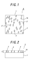
- Fig. 1 is a plan view conceptually showing a part of a substrate for epitaxial growth according to the present invention
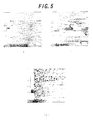
- Fig. 2 is a cross sectional view conceptually showing a part of the epitaxial growth substrate of the present invention.
- the epitaxial growth substrate 5 of the present invention includes the single crystal base 1 and the acicular structure 2 made of AlN formed on the main surface 1A of the base 1.
- the height "h" of the acicular structure 2 is not restricted only if a high crystal quality Al-including III nitride film can be fabricated according to the present invention, but preferably set to 0.5 nm or over, particularly 1 nm or over. In this case, the crystal quality of the desired III nitride film can be enhanced, not dependent on the composition and the thickness of the III nitride film, and the forming condition for the III nitride film.
- the upper limited value of the height "h” of the acicular structure 2 is not limited, but preferably set to 5 nm. If the height "h" of the acicular structure 2 is set beyond the upper limited value, the crystal quality of the desired III nitride film can not be almost enhanced. In addition, with the current forming technique, such a higher acicular structure can not be formed.
- the surface density of the acicular structure 2 is not restricted only if the high quality Al-including III nitride film as desired can be formed, but preferably set 1/ ⁇ m 2 or over, particularly 10/ ⁇ m 2 or over. In this case, the crystal quality of the III nitride film can be enhanced even though the III nitride film includes relatively much Al element.
- the upper limited value of the surface density of the acicular structure 2 is not limited, but preferably set to 1000/ ⁇ m 2 at present. If the surface density of the acicular structure 2 is set beyond the upper limited value, the crystal quality of the III nitride film as desired can not be almost enhanced. In addition, with the current forming technique, such a high surface density acicular structure can not be formed.
- the acicular structure 2 can be formed by a surface treatment for the base 1, for example.
- the acicular structure 2 can be formed by setting and heating the base 1 in a reductive nitrogen-including atmosphere.
- the acicular structure 2 can be formed by means of a surface treatment using a chloride-based gas or a fluorine-based gas. The surface treatment condition is selected appropriately on the sort of the base 1, and the height and the surface density of the acicular structure 2.
- the acicular structure 2 can be formed by means of a CVD method using an Al raw material gas such as trimetylaluminum (TMA) or triethylaluminum (TEA) and a nitrogen raw material gas such as ammonia (NH 3 ) gas.
- TMA trimetylaluminum
- TEA triethylaluminum
- NH 3 ammonia
- the CVD condition is controlled on the sort of the base 1, and the height and the surface density of the acicular structure 2.
- the acicular structure 2 can be fabricated separatedly. In this case, the thus obtained acicular micro crystals are dispersed on the main surface 1A of the base 1.
- the acicular structure 2 may contain B, In, Si, Ge, Be, Mg, Zn, H, C, O or the like. Moreover, the acicular structure 2 may contain inevitable minute element and minute impurities depending on the film-forming condition, the supply source, the base and the reactor material constituting the tubes, the reactor or the susceptor, in addition to the above-mentioned intentional elements.
- the base 1 may be made of a single crystal oxide such as sapphire single crystal, ZnO single crystal, LiAlO 2 single crystal, LiGaO 2 single crystal, MgAl 2 O 4 single crystal, or MgO single crystal, a IV single crystal or a IV-IV single crystal such as Si single crystal or SiC single crystal, a III-V single crystal such as GaAs single crystal, AlN single crystal, GaN single crystal or AlGaN single crystal, and a boride single crystal such as ZrB 2 .
- a single crystal oxide such as sapphire single crystal, ZnO single crystal, LiAlO 2 single crystal, LiGaO 2 single crystal, MgAl 2 O 4 single crystal, or MgO single crystal
- a IV single crystal or a IV-IV single crystal such as Si single crystal or SiC single crystal
- a III-V single crystal such as GaAs single crystal, AlN single crystal, GaN single crystal or AlGaN single crystal
- boride single crystal such as ZrB
- the base 1 may include, on an underbase made of a single crystal as mentioned above, an epitaxial growth film which is made of a single crystal oxide such as ZnO single crystal or MgO single crystal, a IV single crystal or a IV-IV single crystal such as Si single crystal or SiC single crystal, a III-V single crystal such as GaAs single crystal or InP, or the mixture thereof.
- a single crystal oxide such as ZnO single crystal or MgO single crystal
- a IV single crystal or a IV-IV single crystal such as Si single crystal or SiC single crystal
- a III-V single crystal such as GaAs single crystal or InP, or the mixture thereof.
- a desired Al-including III nitride film is formed on the epitaxial growth substrate 5 as illustrated in Figs. 1 and 2. Namely, the III nitride film is formed on the main surface 1A of the base 1 via the acicular structure 2. As a result, the crystallinity and the dislocation density of the III nitride film can be developed and thus, the III nitride film can have excellent crystal quality.
- the FWHM at (102) reflection in X-ray rocking curve can be enhanced to 2000 seconds or below, particularly 1500 seconds or below while the FWHM at (002) reflection in X-ray rocking curve can be enhanced to 100 seconds or below.
- the dislocation density can be reduced to 5 ⁇ 10 10 /cm 2 or below, particularly 1 ⁇ 10 10 /cm 2 or below.
- the III nitride film can be formed by means of a CVD method.
- the epitaxial growth substrate 5 as illustrated in Figs. 1 and 2 is set in a CVD reactor and heated to a predetermined temperature. Then, an Al raw material gas such as TMA or TEA and a nitrogen raw material gas such as NH 3 gas are introduced into the CVD reactor and supplied onto the epitaxial growth substrate 5.
- TMG trimetyl-gallium
- TMI trimetylindium
- the epitaxial growth substrate 5 is preferably heated to 1100°C or over, particularly 1150°C or over. Thereby, the crystallinity of the III nitride film can be more enhanced.
- the above-mentioned temperature means a substrate surface temperature on which the III nitride film is formed.
- the upper limited heating temperature of the epitaxial growth substrate 5 is set to 1250°C or below. If the epitaxial growth substrate 5 is heated beyond the upper limited value, the crystallinity of the III nitride film to be formed can not be almost enhanced. In addition, the surface of the III nitride film may be roughed, resulting in the deterioration of the crystal quality of the III nitride film.
- the thickness of the Al-including III nitride film is preferably set to 0.5 ⁇ m or over, particularly within 1-3 ⁇ m. In this case, the crystallinity of the III nitride film can be more enhanced while the crack creation and the flaking from the epitaxial growth substrate of the III nitride film are prevented.
- the III nitride film includes Al element.
- the Al content of the III nitride film is preferably set to at least 50 atomic percentages for all of the III elements therein. Particularly, it is desired that the III nitride film is made of AlN (100 atomic percentages of Al content).
- This invention is suitable for fabricating any kind of Al-including III nitride film, but the effect/function according to the present invention can be exhibited remarkably as the Al content of the III nitride film is increased.
- the acicular structure 2 can not be observed apparently after the Al-including III nitride film is formed on the epitaxial growth substrate 5 via the acicular structure 2.
- the existence of the acicular structure 2 is surmised from the sharp boundary surface between the single crystal base 1 constituting the epitaxial growth substrate 5 and the III nitride film. It is important to form the acicular structure 2 so that the boundary surface between the base 1 and the III nitride film becomes sharp. In this case, dislocations, which is originated from the mismatch in lattice constant between the base 1 and the III nitride film, can be aligned in the boundary surface, so that the creation of dislocation can be repressed.
- the III nitride film may contain another III element such as Ga element or In element except Al element. Then, the III nitride film may contain additional element such as Ge, Si, Mg, Zn, Be, P or B as occasion demands. Moreover, the III nitride film may contain inevitable minute element and minute impurities depending on the film-forming condition, the supply source and the reactor material.
- Fig. 3 is a structural view showing a PIN-type semiconductor light-emitting element including an epitaxial growth substrate according to the present invention.
- the underlayer 12 on the substrate 11 are formed in turn the underlayer 12, the n-type conductive layer 13, the light-emitting layer (active layer) 14, the p-type cladding layer 15 and the p-type conductive layer 16.
- the n-type conductive layer 13 is partially removed, and then, the main surface of the layer 13 is partially exposed.
- the n-type electrode 17 made of Al/Ti, etc. is formed on the exposed main surface of the layer 13, and the p-type electrode 18 made of Au/Ni, etc. is formed on the p-type conductive layer 16.
- the n-type electrode 17 and the p-type electrode 18 When a given voltage is applied between the n-type electrode 17 and the p-type electrode 18, the recombination of carriers is created to generate and emit a given light.
- the wavelength of the emitted light is determined on the structure and the composition of the light-emitting layer 14.
- the substrate 11 is made of an epitaxial growth substrate as shown in Figs. 1 and 2 according to the present invention.
- the underlayer 12 is made of an Al-including III nitride film as mentioned above. Therefore, the underlayer 12 must satisfy the above-mentioned requirements for the III nitride film.
- the Al contents of the n-type conductive layer 13 through the p-type conductive layer 16 which are formed on the underlayer 12 are preferably set larger than the Al content of the underlayer 12 by 0.5 or over, particularly 0.8 or over at mole ratio. In this case, the dislocation densities of the n-type conductive layer 13 through the p-type conductive layer 16 can be reduced effectively. More preferably, the n-type conductive layer 13 through the p-type conductive layer 16 are made of III nitrides not including Al element. In this case, the dislocation density reduction becomes more conspicuous.
- the substrate 11 is made of an epitaxial growth substrate according to the present invention and the underlayer 12 is made of a high crystal quality Al-including III nitride film fabricated according to the present invention, the crystal qualities of the n-type conductive layer 13 through the p-type conductive layer 16 can be developed, so that the semiconductor light-emitting element 20 can exhibit a high luminous efficiency.
- the underlayer 12 through the p-type conductive layer 16 can be fabricated through epitaxial growth by means of a MOCVD method, for example.
- a c-faced sapphire single crystal was employed as a base, and then, set and attracted on a susceptor installed in a reactor. Thereafter, the base was heated to 1150°C and held for ten minutes with flowing a hydrogen gas at a total amount of 10 slm, thereby to clean the main surface of the base. Then, an NH 3 gas was introduced into the reactor and supplied onto the base at a flow rate of 1000 sccm, a total amount of 5 slm and a pressure of 20 Torr for 0.5 minutes, three minutes and five minutes, respectively, to perform three different surface treatments for the main surface of the base.
- Figs. 4 and 5 are AFM images showing the surface conditions of the main surface of the base as the three different surface treatments are performed.
- Fig. 4 shows AFM images within 1 ⁇ m square region
- Fig. 5 shown AFM images within 5 ⁇ m square region.
- Fig. 4(a) and Fig. 5(a) correspond to AFM images at the surface treatment for 0.5 minutes
- Fig. 4(b) and Fig. 5(b) correspond to AFM images at the surface treatment for three minutes
- Figs. 4(c) and Fig. 5(c) correspond to AFM images at the surface treatment for five minutes.
- white spots correspond to acicular structure.
- acicular structures are formed on the main surface of the base by the above-mentioned surface treatments. Then, the surface density of the acicular structures is increased with the period of the surface treatment.
- the cross section of the resulting multilayered structure was observed by mean of TEM, in order to observe the atomic image for the boundary surface between the AlN film and the base. It was turned out from the TEM observation that boundary surface roughness was reduced to three atomic steps or below within 100 nm region, and thus, the boundary surface was sharp. Dislocations originated from lattice mismatch were observed at nearly equal space of every seven or eight atomic layers of the AlN layer.
- Fig. 6 shows the cross sectional TEM image.
- the temperature of the base was set to 1120°C, and a TMA, an NH 3 and a SiH 4 were flowed at a total gas average flow rate of 1m/sec under a normal pressure, to form a Si-doped n-Al 0.05 Ga 0.95 N layer in a thickness of 3 ⁇ m as an n-type conductive layer.
- the film forming rate was set to 3 ⁇ m/hr by controlling the supply amount of the raw material gases.
- the SiH 4 was supplied so that the carrier density of the n-Al 0.05 Ga 0.95 N layer was set to 5 ⁇ 10 17 /cm 3 .
- a nitrogen carrier gas was flowed instead of the above hydrogen carrier gas.
- the temperature of the base was set to 700°C.
- a TMI, a TMG and an NH 3 were supplied onto the n-Al 0.05 Ga 0.95 N layer at a total gas flow rate of 1m/sec, to form a MQW structured light-emitting layer made of i-GaN layer.
- a TMA was switched for the TMI, and a Cp 2 Mg was supplied, to form a p-Al 0.15 Ga 0.85 N layer in a thickness of 20 nm as a p-type cladding layer.
- the carrier density of the p-Al 0.15 Ga 0.85 N layer was set to 2 ⁇ 10 17 /cm 3 by controlling the flow rate of the Cp 2 Mg. Thereafter, the supply of the TMA was stopped, and the base was heated to 1100°C. Then, a TMG, an NH 3 and Cp 2 Mg were supplied onto the p-Al 0.15 Ga 0.85 N layer, to form a Mg-doped Al 0.05 Ga 0.95 N layer in a thickness of 0.2 ⁇ m.
- Fig. 7 shows the cross sectional TEM image.
- the dislocation density of the AlN film formed on the base via the acicular structure is reduced, as being compared with the AlN film formed not via the acicular structure.
- the crystallinity of the AlN film formed via the acicular structure is enhanced, as being compared with the AlN film not via the acicular structure.
- the FWHM at (102) reflection in X-ray rocking curve is developed to 100 seconds or below while the FWHM at (002) reflection in X-ray rocking curve is developed to 2000 seconds or below.
- a buffer layer or a multi-layered structure such as a distorted superstructure may be provided on the base.
- the crystallinity of the Al-including III nitride film to be formed can be developed.
- a new method for fabricating a III nitride film whereby a high crystal quality Al-including III nitride film can be formed on a given single crystal base can be provided. And a new substrate for epitaxial growth whereby the high crystal quality Al-including III nitride film can be formed can be provided. Moreover, the high crystal quality Al-including III nitride film which is preferably usable for a semiconductor element can be provided.
- An acicular structure is formed of AlN on the main surface of a base made of single crystal. Then, a desired Al-including III nitride film is formed on the main surface of the base via the acicular structure.
Landscapes
- Chemical & Material Sciences (AREA)
- Engineering & Computer Science (AREA)
- Crystallography & Structural Chemistry (AREA)
- Materials Engineering (AREA)
- Metallurgy (AREA)
- Organic Chemistry (AREA)
- Chemical Kinetics & Catalysis (AREA)
- General Chemical & Material Sciences (AREA)
- Inorganic Chemistry (AREA)
- Crystals, And After-Treatments Of Crystals (AREA)
- Led Devices (AREA)
- Chemical Vapour Deposition (AREA)
Applications Claiming Priority (6)
| Application Number | Priority Date | Filing Date | Title |
|---|---|---|---|
| JP2001390844 | 2001-12-25 | ||
| JP2001390844 | 2001-12-25 | ||
| JP2002080745 | 2002-03-22 | ||
| JP2002080745 | 2002-03-22 | ||
| JP2002257864A JP3831322B2 (ja) | 2001-12-25 | 2002-09-03 | Iii族窒化物膜の製造方法、エピタキシャル成長用基板、iii族窒化物膜、iii族窒化物素子用エピタキシャル基板、及びiii族窒化物素子 |
| JP2002257864 | 2002-09-03 |
Publications (3)
| Publication Number | Publication Date |
|---|---|
| EP1323851A2 true EP1323851A2 (fr) | 2003-07-02 |
| EP1323851A3 EP1323851A3 (fr) | 2006-09-06 |
| EP1323851B1 EP1323851B1 (fr) | 2015-07-01 |
Family
ID=27347989
Family Applications (1)
| Application Number | Title | Priority Date | Filing Date |
|---|---|---|---|
| EP02028869.2A Expired - Lifetime EP1323851B1 (fr) | 2001-12-25 | 2002-12-23 | Procédé pour la production des films du type III-nitrure |
Country Status (3)
| Country | Link |
|---|---|
| US (1) | US6749957B2 (fr) |
| EP (1) | EP1323851B1 (fr) |
| JP (1) | JP3831322B2 (fr) |
Cited By (1)
| Publication number | Priority date | Publication date | Assignee | Title |
|---|---|---|---|---|
| EP1975984A3 (fr) * | 2007-03-30 | 2013-04-03 | Fujitsu Ltd. | Dispositif à semi-conducteur de composé comportant une couche AIN d'asymétrie contrôlée |
Families Citing this family (5)
| Publication number | Priority date | Publication date | Assignee | Title |
|---|---|---|---|---|
| KR100646696B1 (ko) * | 2004-03-10 | 2006-11-23 | 주식회사 실트론 | 질화물 반도체 소자 및 그 제조방법 |
| JP4712450B2 (ja) * | 2004-06-29 | 2011-06-29 | 日本碍子株式会社 | AlN結晶の表面平坦性改善方法 |
| US20080150064A1 (en) * | 2006-12-12 | 2008-06-26 | Zimmerman Michael A | Plastic electronic component package |
| KR101317735B1 (ko) * | 2009-09-07 | 2013-10-15 | 도꾸리쯔교세이호징 리가가쿠 겐큐소 | 질화물 반도체 다층 구조체 및 그 제조 방법과, 질화물 반도체 발광 소자 |
| CN102054916B (zh) * | 2010-10-29 | 2012-11-28 | 厦门市三安光电科技有限公司 | 反射器及其制作方法,以及包含该反射器的发光器件 |
Citations (1)
| Publication number | Priority date | Publication date | Assignee | Title |
|---|---|---|---|---|
| EP1065705A2 (fr) | 1999-06-30 | 2001-01-03 | Toyoda Gosei Co., Ltd. | Composant semi-conducteur composé de nitrure du groupe III et procédé de sa fabrication |
Family Cites Families (12)
| Publication number | Priority date | Publication date | Assignee | Title |
|---|---|---|---|---|
| JPH07144920A (ja) * | 1993-09-08 | 1995-06-06 | Takeshi Masumoto | 窒化物複合超微粒子及びその製造方法と超微粒子焼結体 |
| JPH07138086A (ja) * | 1993-11-15 | 1995-05-30 | Toshiba Corp | 表面導電性窒化アルミニウム基体およびその製造方法 |
| JPH07235692A (ja) * | 1993-12-30 | 1995-09-05 | Sony Corp | 化合物半導体装置及びその形成方法 |
| US5656832A (en) * | 1994-03-09 | 1997-08-12 | Kabushiki Kaisha Toshiba | Semiconductor heterojunction device with ALN buffer layer of 3nm-10nm average film thickness |
| KR100304881B1 (ko) * | 1998-10-15 | 2001-10-12 | 구자홍 | Gan계화합물반도체및그의결정성장방법 |
| US6495894B2 (en) * | 2000-05-22 | 2002-12-17 | Ngk Insulators, Ltd. | Photonic device, a substrate for fabricating a photonic device, a method for fabricating the photonic device and a method for manufacturing the photonic device-fabricating substrate |
| JP2002124472A (ja) * | 2000-10-13 | 2002-04-26 | Ngk Insulators Ltd | Iii族窒化物膜の製造方法 |
| JP2002222771A (ja) * | 2000-11-21 | 2002-08-09 | Ngk Insulators Ltd | Iii族窒化物膜の製造方法、iii族窒化物膜の製造用下地膜、及びその下地膜の製造方法 |
| JP4001262B2 (ja) * | 2001-02-27 | 2007-10-31 | 日本碍子株式会社 | 窒化物膜の製造方法 |
| JP4209097B2 (ja) * | 2001-05-24 | 2009-01-14 | 日本碍子株式会社 | 半導体受光素子 |
| JP4260380B2 (ja) | 2001-06-12 | 2009-04-30 | 日本碍子株式会社 | Iii族窒化物膜の製造方法、iii族窒化物膜製造用サファイア単結晶基板、及びエピタキシャル成長用基板 |
| JP3954335B2 (ja) * | 2001-06-15 | 2007-08-08 | 日本碍子株式会社 | Iii族窒化物多層膜 |
-
2002
- 2002-09-03 JP JP2002257864A patent/JP3831322B2/ja not_active Expired - Lifetime
- 2002-12-18 US US10/321,658 patent/US6749957B2/en not_active Expired - Lifetime
- 2002-12-23 EP EP02028869.2A patent/EP1323851B1/fr not_active Expired - Lifetime
Patent Citations (1)
| Publication number | Priority date | Publication date | Assignee | Title |
|---|---|---|---|---|
| EP1065705A2 (fr) | 1999-06-30 | 2001-01-03 | Toyoda Gosei Co., Ltd. | Composant semi-conducteur composé de nitrure du groupe III et procédé de sa fabrication |
Non-Patent Citations (1)
| Title |
|---|
| HEINLEIN ET AL., J. APPL. PHYS., vol. 83, 1998, pages 6023 |
Cited By (2)
| Publication number | Priority date | Publication date | Assignee | Title |
|---|---|---|---|---|
| EP1975984A3 (fr) * | 2007-03-30 | 2013-04-03 | Fujitsu Ltd. | Dispositif à semi-conducteur de composé comportant une couche AIN d'asymétrie contrôlée |
| US8440549B2 (en) | 2007-03-30 | 2013-05-14 | Fujitsu Limited | Compound semiconductor device including aln layer of controlled skewness |
Also Published As
| Publication number | Publication date |
|---|---|
| JP2004006587A (ja) | 2004-01-08 |
| US20030124393A1 (en) | 2003-07-03 |
| JP3831322B2 (ja) | 2006-10-11 |
| EP1323851B1 (fr) | 2015-07-01 |
| US6749957B2 (en) | 2004-06-15 |
| EP1323851A3 (fr) | 2006-09-06 |
Similar Documents
| Publication | Publication Date | Title |
|---|---|---|
| US6462357B1 (en) | Epitaxial growth of nitride compound semiconductor | |
| US20030219634A1 (en) | Method for fabricating a III nitride film, an underlayer for fabricating a III nitride film and a method for fabricating the same underlayer | |
| EP1335435B1 (fr) | Dispositifs semi-conducteurs électroluminescents | |
| US20020104998A1 (en) | Semiconductor light-emitting element | |
| US8143154B2 (en) | Relaxed InGaN/AlGaN templates | |
| EP1673815B1 (fr) | Élément semi-conducteur en nitrures du groupe iii et dispositifs semi-conducteurs l'incorporant | |
| US7067847B2 (en) | Semiconductor element | |
| US6759715B2 (en) | Epitaxial base substrate and epitaxial substrate | |
| US7550368B2 (en) | Group-III nitride semiconductor stack, method of manufacturing the same, and group-III nitride semiconductor device | |
| KR20020050174A (ko) | 반도체의 제조방법, 반도체기판의 제조방법 및 반도체발광소자 | |
| US7172956B2 (en) | Substrate for semiconductor light-emitting element, semiconductor light-emitting element and semiconductor light-emitting element fabrication method | |
| US6749957B2 (en) | Method for fabricating a III nitride film, substrate for epitaxial growth, III nitride film, epitaxial growth substrate for III nitride element and III nitride element | |
| US6821807B2 (en) | Method of forming nitride-based semiconductor layer, and method of manufacturing nitride-based semiconductor device | |
| JP4624064B2 (ja) | Iii族窒化物半導体積層物 | |
| EP1869717B1 (fr) | Procédé de production d'un élément semi-conducteur à base d'un nitrure du groupe iii | |
| JP4514727B2 (ja) | Iii族窒化物膜の製造方法、iii族窒化物膜、iii族窒化物素子用エピタキシャル基板、及びiii族窒化物素子 | |
| JP4107889B2 (ja) | 半導体素子の製造方法 |
Legal Events
| Date | Code | Title | Description |
|---|---|---|---|
| PUAI | Public reference made under article 153(3) epc to a published international application that has entered the european phase |
Free format text: ORIGINAL CODE: 0009012 |
|
| AK | Designated contracting states |
Designated state(s): AT BE BG CH CY CZ DE DK EE ES FI FR GB GR IE IT LI LU MC NL PT SE SI SK TR |
|
| AX | Request for extension of the european patent |
Extension state: AL LT LV MK RO |
|
| PUAL | Search report despatched |
Free format text: ORIGINAL CODE: 0009013 |
|
| AK | Designated contracting states |
Kind code of ref document: A3 Designated state(s): AT BE BG CH CY CZ DE DK EE ES FI FR GB GR IE IT LI LU MC NL PT SE SI SK TR |
|
| AX | Request for extension of the european patent |
Extension state: AL LT LV MK RO |
|
| 17P | Request for examination filed |
Effective date: 20070221 |
|
| AKX | Designation fees paid |
Designated state(s): DE FR GB |
|
| 17Q | First examination report despatched |
Effective date: 20100709 |
|
| REG | Reference to a national code |
Ref country code: DE Ref legal event code: R079 Ref document number: 60247281 Country of ref document: DE Free format text: PREVIOUS MAIN CLASS: C30B0025020000 Ipc: H01L0021020000 |
|
| RIC1 | Information provided on ipc code assigned before grant |
Ipc: C30B 25/18 20060101ALI20140702BHEP Ipc: C30B 25/02 20060101ALI20140702BHEP Ipc: C30B 29/40 20060101ALI20140702BHEP Ipc: H01L 33/00 20100101ALI20140702BHEP Ipc: H01L 21/02 20060101AFI20140702BHEP |
|
| GRAP | Despatch of communication of intention to grant a patent |
Free format text: ORIGINAL CODE: EPIDOSNIGR1 |
|
| INTG | Intention to grant announced |
Effective date: 20141216 |
|
| GRAP | Despatch of communication of intention to grant a patent |
Free format text: ORIGINAL CODE: EPIDOSNIGR1 |
|
| INTG | Intention to grant announced |
Effective date: 20150316 |
|
| GRAS | Grant fee paid |
Free format text: ORIGINAL CODE: EPIDOSNIGR3 |
|
| GRAA | (expected) grant |
Free format text: ORIGINAL CODE: 0009210 |
|
| AK | Designated contracting states |
Kind code of ref document: B1 Designated state(s): DE FR GB |
|
| REG | Reference to a national code |
Ref country code: GB Ref legal event code: FG4D |
|
| REG | Reference to a national code |
Ref country code: DE Ref legal event code: R096 Ref document number: 60247281 Country of ref document: DE |
|
| REG | Reference to a national code |
Ref country code: FR Ref legal event code: PLFP Year of fee payment: 14 |
|
| REG | Reference to a national code |
Ref country code: DE Ref legal event code: R097 Ref document number: 60247281 Country of ref document: DE |
|
| PLBE | No opposition filed within time limit |
Free format text: ORIGINAL CODE: 0009261 |
|
| STAA | Information on the status of an ep patent application or granted ep patent |
Free format text: STATUS: NO OPPOSITION FILED WITHIN TIME LIMIT |
|
| 26N | No opposition filed |
Effective date: 20160404 |
|
| REG | Reference to a national code |
Ref country code: FR Ref legal event code: PLFP Year of fee payment: 15 |
|
| REG | Reference to a national code |
Ref country code: FR Ref legal event code: PLFP Year of fee payment: 16 |
|
| PGFP | Annual fee paid to national office [announced via postgrant information from national office to epo] |
Ref country code: DE Payment date: 20211102 Year of fee payment: 20 Ref country code: GB Payment date: 20211104 Year of fee payment: 20 Ref country code: FR Payment date: 20211115 Year of fee payment: 20 |
|
| REG | Reference to a national code |
Ref country code: DE Ref legal event code: R071 Ref document number: 60247281 Country of ref document: DE |
|
| REG | Reference to a national code |
Ref country code: GB Ref legal event code: PE20 Expiry date: 20221222 |
|
| PG25 | Lapsed in a contracting state [announced via postgrant information from national office to epo] |
Ref country code: GB Free format text: LAPSE BECAUSE OF EXPIRATION OF PROTECTION Effective date: 20221222 |