EP1324059A2 - Vorrichtung und Verfahren zur Feststellung von Lötstellenfehlern - Google Patents
Vorrichtung und Verfahren zur Feststellung von Lötstellenfehlern Download PDFInfo
- Publication number
- EP1324059A2 EP1324059A2 EP02258011A EP02258011A EP1324059A2 EP 1324059 A2 EP1324059 A2 EP 1324059A2 EP 02258011 A EP02258011 A EP 02258011A EP 02258011 A EP02258011 A EP 02258011A EP 1324059 A2 EP1324059 A2 EP 1324059A2
- Authority
- EP
- European Patent Office
- Prior art keywords
- solder
- printed
- solder joints
- joint
- circuit device
- Prior art date
- Legal status (The legal status is an assumption and is not a legal conclusion. Google has not performed a legal analysis and makes no representation as to the accuracy of the status listed.)
- Withdrawn
Links
Images





Classifications
-
- G—PHYSICS
- G01—MEASURING; TESTING
- G01R—MEASURING ELECTRIC VARIABLES; MEASURING MAGNETIC VARIABLES
- G01R31/00—Arrangements for testing electric properties; Arrangements for locating electric faults; Arrangements for electrical testing characterised by what is being tested not provided for elsewhere
- G01R31/28—Testing of electronic circuits, e.g. by signal tracer
- G01R31/2801—Testing of printed circuits, backplanes, motherboards, hybrid circuits or carriers for multichip packages [MCP]
- G01R31/281—Specific types of tests or tests for a specific type of fault, e.g. thermal mapping, shorts testing
- G01R31/2812—Checking for open circuits or shorts, e.g. solder bridges; Testing conductivity, resistivity or impedance
-
- G—PHYSICS
- G01—MEASURING; TESTING
- G01N—INVESTIGATING OR ANALYSING MATERIALS BY DETERMINING THEIR CHEMICAL OR PHYSICAL PROPERTIES
- G01N23/00—Investigating or analysing materials by the use of wave or particle radiation, e.g. X-rays or neutrons, not covered by groups G01N3/00 – G01N17/00, G01N21/00 or G01N22/00
- G01N23/02—Investigating or analysing materials by the use of wave or particle radiation, e.g. X-rays or neutrons, not covered by groups G01N3/00 – G01N17/00, G01N21/00 or G01N22/00 by transmitting the radiation through the material
- G01N23/04—Investigating or analysing materials by the use of wave or particle radiation, e.g. X-rays or neutrons, not covered by groups G01N3/00 – G01N17/00, G01N21/00 or G01N22/00 by transmitting the radiation through the material and forming images of the material
-
- G—PHYSICS
- G01—MEASURING; TESTING
- G01N—INVESTIGATING OR ANALYSING MATERIALS BY DETERMINING THEIR CHEMICAL OR PHYSICAL PROPERTIES
- G01N23/00—Investigating or analysing materials by the use of wave or particle radiation, e.g. X-rays or neutrons, not covered by groups G01N3/00 – G01N17/00, G01N21/00 or G01N22/00
- G01N23/02—Investigating or analysing materials by the use of wave or particle radiation, e.g. X-rays or neutrons, not covered by groups G01N3/00 – G01N17/00, G01N21/00 or G01N22/00 by transmitting the radiation through the material
- G01N23/04—Investigating or analysing materials by the use of wave or particle radiation, e.g. X-rays or neutrons, not covered by groups G01N3/00 – G01N17/00, G01N21/00 or G01N22/00 by transmitting the radiation through the material and forming images of the material
- G01N23/044—Investigating or analysing materials by the use of wave or particle radiation, e.g. X-rays or neutrons, not covered by groups G01N3/00 – G01N17/00, G01N21/00 or G01N22/00 by transmitting the radiation through the material and forming images of the material using laminography or tomosynthesis
Definitions
- the present disclosure relates generally to systems and methods for high-resolution inspection of circuit board assemblies using measurement systems, and in particular, to systems which measure solder joints within circuit board assemblies for quality control analysis.
- the appearance of the X-ray shadow or radiograph is determined not only by the internal structural characteristics of the object, but also by the direction from which the incident X-rays strike the object. Therefore, a complete interpretation and analysis of X-ray shadow images, whether performed visually by a person or numerically by a computer, often requires that certain assumptions be made regarding the characteristics of the object and its orientation with respect to the X-ray beam. For example, it is often necessary to make specific assumptions regarding the shape, internal structure, etc. of the object and the direction of the incident X-rays upon the object.
- features of the X-ray image may be analyzed to determine the location, size, shape, etc., of the corresponding structural characteristic of the object, e.g., a defect in a solder connection, which produced the image feature.
- These assumptions often create ambiguities, which degrade the reliability of the interpretation of the images and the decisions based upon the analysis of the X-ray shadow images.
- some systems incorporate the capability of viewing the object from a plurality of angles.
- the additional views enable these systems to partially resolve the ambiguities present in the X-ray shadow projection images.
- utilization of multiple viewing angles necessitates a complicated mechanical handling system, often requiring as many as five independent, non-orthogonal axes of motion.
- This degree of mechanical complication leads to increased expense, increased size and weight, longer inspection times, reduced throughput, impaired positioning precision due to the mechanical complications, and calibration and computer control complications due to the non-orthogonality of the axes of motion.
- a laminography system which views a fixed object and has an imaging area that is smaller than the object being inspected, it may be necessary to move the object around to position different regions of the object within the imaging area thus generating multiple laminographs, which when pieced together form an image of the entire object.
- This is frequently achieved by supporting the object on a mechanical handling system, such as an X-Y-Z positioning table. The table is then moved to bring the desired regions of the object into the imaging area. Movement in the X and Y directions locates the region to be examined, while movement in the Z direction moves the object up and down to select the plane within the object where the cross-sectional image is taken.
- one technique commonly used for positioning the selected feature of the test object within the cross-sectional image focal plane physically measures the "Z"-axis position of the selected feature. Using this measurement, the test object is then positioned along the "Z" axis such that the selected feature coincides with the "Z"-axis position of the cross-sectional image focal plane. Any of a variety of standard methods and instruments may be used to physically measure the "Z"-axis position of the selected feature of the test object. There are several types of commercially-available Z-ranging systems, which are used to determine the distance between a known location in "Z" and a feature on the surface, or just below the surface, of the test object.
- Such systems may be as simple as a mechanical fixing of the test object, a mechanical probe, a laser-based optical triangulation system, an optical-interferometric system, an ultrasonic system, among others. Any one of these "Z"-axis position measuring systems may be used to form a "Z-map" of the surface of the test object.
- the "Z-map” typically consists of an array of X and Y positions associated array of the Z-values of the surface of the test object.
- the locations i.e., X, Y positions
- the systems most commonly used in systems for cross-sectional image features on printed-circuit boards are laser-based triangulation range finders.
- Range finders have been used in particular for cross-sectional X-ray image systems that are used to image electronic circuit board assemblies.
- Circuit-board assemblies are typically very thin in comparison to the surface area in which the components are mounted.
- Some circuit assemblies are made with very dimensionally-stable material, such as ceramic substrates.
- the majority of circuit-board assemblies are constructed with a material that is somewhat flexible or in some cases very flexible. This flexibility allows the board to develop a warp in the axis perpendicular to the major surface areas (i.e., the surface areas that contain interface pins) or the "Z" dimension. Additionally, some circuit board assemblies have variations in board thickness.
- one such range finder system is designed for use in a system such as that described in U.S. Patent No. 4,926,452 to Baker, et al. Hereafter referred to as the '452 patent.
- the '452 patent discloses a laminography system in which an X-ray based imaging system having a very shallow depth of field is used to examine solid objects such as printed-circuit boards.
- the shallow depth of field provides a means for examining the integrity of a solder joint without interference from the components above and below the solder joint.
- the material above and below the solder joint is out of focus, and hence, contributes to a more or less uniform background.
- the depth of field of the laminographic-imaging system is on the order of less than approximately 2 millionths of an inch (2 mils.).
- surface variations on the printed-circuit board often exceed this tolerance.
- the surface of the printed-circuit board is mapped using a laser-range finder. The detailed laser-range finder generated map is then used to position the circuit board with respect to the X-ray imaging system such that the component of interest is in focus even when the board is translated from one field of interest to another.
- solder-joint inspection systems One disadvantage of solder-joint inspection systems is the methodology used in determining whether a measured solder-joint feature is indicative of a solder joint that is "acceptable” or “defective.”
- Present soider-joint inspection systems apply a pre-set threshold to each solder joint feature in order to make these determinations.
- This methodology for identifying "defective" solder joints is problematic for determining when an individual solder joint on an array package is “defective.” This is especially evident in the accuracy rate of identified "open circuits" for solder joints associated with various array package types.
- Ball-grid array (BGA) circuit packages for example, have a planar-bottom face or mounting surface that is generally either square or rectangular in shape. This face may be covered with small spherical leads that carry electric signals to and from the integrated circuit that is a part of the "chip" or integrated circuit package. As is known, the planar bottom forms part of a substrate (typically a multi-layered substrate) to which an integrated circuit die is affixed.
- a substrate typically a multi-layered substrate
- solder ball i.e., a solder joint
- solder ball i.e., a solder joint
- the package material may warp resulting in a significant variation in the relative distance between the mounting surfaces of the package and a printed-circuit board.
- BGA packages warp such that the edges tend to pull away from the mounting surface of the printed-circuit board (i.e., the edges turn upward).
- BGA-package warp can occur in a host of various ways with the distance between the mounting surfaces of a BGA package and a printed-circuit board varying in a number of different ways across the mounting surfaces.
- Other packages such as, but not limited to column grid array (CGA), flip-chip, chip scale packages (CSPs), and quad flat packs, etc. may also suffer from warp.
- the printed-circuit board material may warp. It should be appreciated that these two conditions are not mutually exclusive of each other. Stated in another way, both the printed-circuit board (i.e., a mounting surface) and the package may be warped. Furthermore, either of the printed-circuit board and/or the package may suffer from "tilt.” A “tilt” condition is present when the mounting surface elevation (i.e., height in the "Z" dimension) varies from one edge to an opposing edge on either a package or a printed-circuit board.
- a printed-circuit assembly may contain a plurality of multi-pin devices (e.g., array packages) with a significant variation in one or more solder-joint measurements.
- multi-pin devices e.g., array packages
- an increase in the distance between the mounting surfaces of the BGA package and the printed-circuit board may cause one or more solder balls to stretch such that its diameter is less than that of the solder ball in its pre-reflow condition.
- the solder balls collapse from their pre-reflow condition. The balls closer to the center of the array typically collapse more than the solder balls closer to the external edges of the array.
- solder-joint measurements may be adequately connected, both structurally and electrically, via the corresponding solder-joint. Any associated differences in the various measurements of the solder-joints (in those situations where corresponding conductors are adequately connected) is representative of an acceptable variation across the plurality of solder-joint measurements.
- solder-joint inspection systems for BGA devices has been problematic. Not only is it time consuming to rework each BGA package identified as having one or more "defective" solder-joint test results, short of a full functional test of the printed-circuit assembly (i.e., a completely populated printed-circuit board), or in-circuit test of the part, which requires 100% electrical test access, no non-destructive verification method exists to independently confirm the accuracy of the defect conclusion.
- oval shaped pads In response, some manufacturers have used oval shaped pads with various printed-circuit devices.
- the oval shaped pads cause solder balls to form oval shaped solder joints when the pad is properly bonded by the solder.
- the oval shaped pads permit detection of "open" solder joints as the associated solder image remains circular.
- solder-joint inspection system records location information regarding a plurality of pins (i.e., solder-joint interfaces) on each printed-circuit device of a printed-circuit assembly (i.e., a device populated printed-circuit board) as well as information regarding the variation in distance between the mounting surface of the printed-circuit assembly, and device package.
- the solder-joint inspection system generates an expected pass/fail criteria for each solder joint that accounts for acceptable variation in actual measurement values recorded for the set of solder joints on each printed-circuit device.
- an improved solder-joint inspection system can be realized with a means for measuring a solder joint; a means for computing; and a data storage means.
- Some embodiments of the system can be viewed as providing a method for identifying solder joint defects.
- the method can be summarized by the following steps: recording a measurement of each solder joint on a printed-circuit assembly; estimating an expected value for each of the solder joints that accounts for acceptable variance in elevation of the printed-circuit device with respect to a printed-circuit board; comparing the recorded measurement with the expected value for each solder joint to generate a error value for each solder joint; and identifying measurement error outliers.
- the method can be summarized by the following steps: acquiring location information for a plurality of pins on a printed-circuit device; obtaining information indicative of height variation across a mounting surface of the printed-circuit device; recording a measurement of a plurality of solder joints associated with the plurality of pins; estimating a range of acceptable measurements for respective solder joints responsive to the height variation across the mounting surface; and setting at least one threshold responsive to a limit of the range.
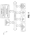
- FIG. 1 is a block diagram of an exemplar circuit inspection system.
- FIG. 2 is a plot of solder joint diameter values for an exemplar ball-grid array device.
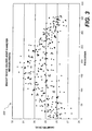
- FIG. 3 is a plot of solder joint diameter values for another exemplar ball-grid array device.
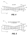
- FIG. 4 is a side-view illustrating the effect of ball-grid array warp on individual solder joint diameters.
- FIG. 5 is a side-view illustrating the effect of ball-grid array warp coupled with printed-circuit board tilt and warp on individual solder joint diameters.
- FIG. 6 is a plan-view of an exemplar ball-grid array device illustrating a method for determining the distance from a centroid of a device for two solder joints.
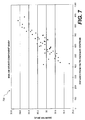
- FIG. 7 is an exemplar plot of solder joint diameter values versus solder joint (pin) distance from a package centroid.
- FIG. 8 is a second exemplar plot of solder joint diameter values versus solder joint (pin) distance form a package centroid.
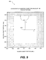
- FIG. 9 is an exaggerated plan-view of solder joint diameters for a first arrangement of solder joints on an exemplar ball-grid array package.
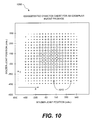
- FIG. 10 is an exaggerated plan-view of solder joint diameters for a second arrangement of solder joints on an exemplar ball-grid array package.
- FIG. I is a schematic illustrating the association of identified solder joints on an exemplar ball-grid array package with its neighboring solder joints that may be applied by the circuit inspection system of FIG. 1.
- FIG. 12 is a plot of near neighbor solder joint diameter errors sorted by package type and error size that may be created by dated recorded by the circuit inspection system of FIG. 1.
- FIG. 13 is a plot illustrating a near neighbor solder-joint diameter errors outlier analysis that may be applied by the circuit inspection system of FIG. 1.
- FIG. 14 is a flow diagram that illustrates a method for adapting test thresholds that may be practiced by the circuit inspection system of FIG. 1.
- FIG. 15 is a functional block diagram illustrating various exemplar components of the solder joint analysis application of FIG. 1.
- FIG. 16 is a flow diagram that illustrates a method for identifying solder-joint defects that may be practiced by the circuit inspection system of FIG. 1.
- the present invention is directed to a system and method, which addresses the above listed problems. Particularly important is that an improved solder-joint inspection system configured to apply the method for adapting test thresholds may significantly reduce the number of false "defects" identified upon analyzing one or more measurements of each individual solder joint.
- An improved solder-joint inspection system configured in accordance with the method for adapting test thresholds accounts for acceptable variation in the distance between the mounting surfaces of a printed-circuit device package and a printed-circuit board when setting pass/fail criteria. More specifically, the method for adapting test thresholds accepts low-frequency variation in measured parameters of adjacent solder joints across the mounting surface of the printed-circuit device, while identifying high-frequency variation between adjacent solder joints.
- the exemplar data, figures, and related description are focused on diameter measurements associated with solder joints affixed to BGA packages.
- Those skilled in the art will appreciate that low-frequency variation occurs in other solder joint types (i.e., non-spherical joints) at least due to the same reasons that cause BGA packages and printed-circuit boards to warp. Consequently, the method for adapting test thresholds will be applicable to various other solder joint types.
- a commercially-available solder-joint inspection system such as the 5DX X-ray Inspection System available from Agilent Technologies of Palo Alto, California, records location information regarding a plurality of pins (i.e., solder-joint interfaces) on each printed-circuit device of a printed-circuit assembly (i.e., a device populated printed-circuit board). Using the location information, the solder-joint inspection system associates each of the plurality of pins with a set of neighbor pins (i.e., adjacent pins) on each respective printed-circuit device.
- a set of neighbor pins i.e., adjacent pins
- the solder-joint inspection system After recording at least one actual measurement of a characteristic of each solder joint under inspection, the solder-joint inspection system generates an expected pass/fail criteria for each measurement associated with each respective solder joint that accounts for acceptable (i.e., low-frequency) variation in the actual measurement values recorded.
- acceptable (i.e., low-frequency) variation in the actual measurement values recorded exemplary characteristics of a solder joint that may be measured may include thickness, shape, heel height, solder volume, among others.
- estimating techniques may be used to identify individualized expected values for each pin of a printed-circuit device. For example, one embodiment uses a statistical value derived from a set of adjacent solder joint measurements to estimate an expected measurement of a present solder joint under test. Statistical values may include an average, a mean, a median, etc. In a variation of this first embodiment, measurements recorded from across the mounting surface may be sampled when estimating the expected values. In other words, the estimated values for each solder joint used to couple a 100 pin device could be determined from actual measurements from a subset of solder joints across the 100 pin device.
- a second embodiment performs a two-dimensional polynomial fit over the measurement data to identify an expected measurement value for a solder joint under test.
- a third embodiment employs a Fourier analysis over the measured results to identify high-frequency variations between adjacent solder joints. An inverse Fourier transform can be used to identify an expected measurement value for specific solder joints.
- the solder-joint inspection system can perform a comparison of the actual measured value for each particular solder joint of interest with the associated expected value to generate an error value. After an error value is associated with respective solder joints under test on each printed-circuit device, an outlier analysis can be performed to derive a custom pass/fail criteria for each solder joint.
- FIG. 1 is a schematic illustrating the various functional building blocks of a computer-based solder-joint inspection system, which can apply the various methods for identifying solder-joint defects.
- the solder-joint inspection system 100 can comprise any one of a wide variety of wired and/or wireless computing devices, such as a desktop computer, a portable computer, a dedicated server computer, a multi-processor computing device, among others.
- the solder-joint inspection system 100 can, for instance, comprise a processing device 102, memory 110, one or more user interface devices 120, a display 130, one or more input/output (I/O) devices 140, and one or more network interface devices 150, each of which is connected via a local interface 118.
- the processing device 102 can include any custom made or commercially available processor, a central processing unit (CPU) or an auxiliary processor among several processors associated with the solder-joint inspection system 100, a semiconductor based microprocessor (in the form of a microchip), a macro-processor, one or more application-specific integrated circuits (ASICs), a plurality of suitably configured digital logic gates, and other well known electrical configurations comprising discrete elements both individually and in various combinations to coordinate the overall operation of the solder-joint inspection system 100.
- CPU central processing unit
- ASICs application-specific integrated circuits
- the memory 110 can include any one of a combination of volatile memory elements (e.g., random access memory (RAM, such as DRAM, SRAM, etc.)) and non-volatile memory elements (e.g., ROM, hard drive, tape, CDROM, etc.).
- volatile memory elements e.g., random access memory (RAM, such as DRAM, SRAM, etc.)
- non-volatile memory elements e.g., ROM, hard drive, tape, CDROM, etc.
- the memory 110 typically comprises an O/S 112, one or more applications such as a solder-joint analysis application 114.
- the memory 110 can, and typically will, comprise other components, which have been omitted for purposes of brevity. These may include a host of programs configured to control various aspects of the solder-joint inspection mechanisms.
- the one or more user interface devices 120 comprise those components with which the user can interact with the solder-joint inspection system 100.
- the solder-joint inspection system 100 comprises a personal computer (PC)
- these components can comprise a keyboard and mouse.
- the solder-joint inspection system 100 is expected to be used in extreme environments (e.g., near a solder flow machine)
- these components can comprise function keys or buttons, a touch-sensitive screen, a stylus, etc.
- the display 130 can comprise a computer monitor or plasma screen for a PC or alternatively a liquid crystal display (LCD) as may be desired.
- LCD liquid crystal display
- the one or more I/O devices 140 are adapted to facilitate connection of the solder-joint inspection system 100 to another system and/or device and may therefore include one or more serial, parallel, small computer system interface (SCSI), universal serial bus (USB), IEEE 1394 (e.g., FirewireTM), and/or other interface components that may be used to communicatively couple the solder-joint inspection system 100 with one or more remote data storage devices for recording test measurement results.
- the network interlace devices 150 comprise the various components used to transmit and/or receive data over a network.
- the network interface devices 150 may include a device that can communicate both inputs and outputs, for instance, a modulator/demodulator (e.g., a modem), wireless (e.g., a radio-frequency (RF)) transceiver, a telephonic interface, a bridge, a router, a network card, etc.
- a modulator/demodulator e.g., a modem
- wireless e.g., a radio-frequency (RF) transceiver
- a telephonic interface e.g., a telephonic interface
- bridge e.g., a bridge, a router, a network card, etc.
- Various software and/or firmware will be used to manage, coordinate, measure, record, estimate and compare expected values with measured values to generate error values, as well as to perform an outlier analysis on the generated error values, among other functions.
- the related software and/or firmware responsible for theses and other functions associated with the use of the underlying solder-joint inspection system 100 can be stored on any computer-readable medium for use by or in connection with any computer-related system or method.
- a computer-readable medium denotes an electronic, magnetic, optical, or other physical device or means that can contain or store a computer program for use by or in connection with a computer-related system or method.
- programs can be embodied in any computer-readable medium for use by or in connection with an instruction execution system, apparatus, or device, such as a computer-based system, processor-containing system, or other system that can fetch the instructions from the instruction execution system, apparatus, or device and execute the instructions.
- a "computer-readable medium” can be any means that can store, communicate, propagate, or transport the program for use by or in connection with the instruction execution system, apparatus, or device.
- the computer-readable medium can be, for example but not limited to, an electronic, magnetic, optical, electromagnetic, infrared, or semiconductor system, apparatus, device, or propagation medium. More specific examples (a non-exhaustive list) of the computer-readable medium include an electrical connection having one or more wires, a portable computer diskette, a random access memory (RAM), a read-only memory (ROM), an erasable programmable read-only memory (EPROM), an electrically erasable programmable read-only memory (EEPROM), or Flash memory, an optical fiber, and a portable compact disc read-only memory (CDROM).
- RAM random access memory
- ROM read-only memory
- EPROM erasable programmable read-only memory
- EEPROM electrically erasable programmable read-only memory
- CDROM portable compact disc read-only memory
- the computer-readable medium can even be paper or another suitable medium upon which a program is printed, as the program can be electronically captured, via for instance, optical scanning of the paper or other medium, then compiled, interpreted or otherwise processed in a suitable manner as necessary, and then stored in a computer memory.
- FIG. 2 illustrates a plot 200 of sample data points measured and recorded from a particular type of BGA device package.
- the data includes the diameter in mils. for more than 350 solder joints inspected.
- solder joint 210 has a diameter of approximately 30.5 mils and is nearly in the middle of the range of recorded diameters for the BGA package. More specifically, the recorded diameters for individual solder joints range from 29mils. to 31.5mils. for a total variation in diameter of 2.5mils.
- FIG. 3 illustrates a plot 300 of sample data points measured and recorded from another BGA device package type.
- the data includes the diameter in mils. for more than 350 solder joints inspected.
- none of the solder joints is defective.
- the recorded diameters for individual solder joints range from approximately 26.75mils. to 31.5mils, a range of 4.75mils. or nearly twice the range of diameters recorded for solder joints associated with the BGA device represented in FIG. 2.
- a direct application of pass/fail thresholds based solely on individual solder joint diameter measurements may lead to inaccurate defect calls.
- a printed-circuit assembly 400 may comprise a BGA device 410 and a printed-circuit board 420 electrically and physically connected at a plurality of substantially aligned points via a plurality of solder joints 412. It is important to note that the illustration is not to scale. The relative height (i.e., the thickness) of the BGA device 410 and the printed-circuit board 420 used in forming the printed-circuit assembly 400 will often vary and the size of the various solder joints formed by the plurality of solder balls will generally be significantly smaller.
- the BGA device 410 may warp with an upward curve such that opposing ends of the BGA device 410 are "pulled" away from the mounting (i.e., the upper) surface of the printed-circuit board 420.
- the BGA device 410 may warp due to thermal expansion mismatches within the package and/or for other reasons such as stress applied by the printed-circuit board.
- the solder joints 412 cool before the materials in the BGA device 410, thus setting the warp.
- solder joints near the center of the BGA device 410 typically have a larger diameter than solder joints toward the outer edges of the BGA device 410.
- a printed-circuit assembly 500 may comprise a BGA device 510 and a printed-circuit board 520 electrically and physically connected at a plurality of substantially aligned points via a plurality of solder joints 512.
- the printed-circuit assembly 500 of FIG. 5 is not to scale.
- printed-circuit board warp may be non-linear and vary across both the X and Y (i.e., into the page) dimensions. Consequently, the connection points with mounting surfaces (the underside of the BGA device 510 and the upper surface of the printed-circuit board 520) further removed from each other in the "Z" dimension, will have a reduced diameter when measured at the focal plane 550. As previously explained, the resulting wide variation in the measured diameters of solder joints 512 makes it difficult to use this information as the sole indicator of where to place pass/fail criteria for use in the solder-joint inspection system 100 (FIG. 1).
- FIG. 6 illustrates a method for associating the distance from the centroid 610 of an exemplar BGA device 600 with each of the plurality of solder joints 612 located on the mounting surface of the device.
- the solder-joint inspection system 100 can be used to identify a centroid 610 of a particular BGA device 600 presently under test. After having identified the centroid 610 of the BGA device 600 in the X - Y plane, the solder-joint inspection system 100 can be used to determine and store the distance of the center of each respective solder joint 612 from the centroid 610.
- the significance of these distance measurements will be appreciated when observing the sample data plots of FIGs. 7 and 8.
- the data plot 700 illustrated in FIG. 7, arranges the solder joint diameters for the various conducting points of the exemplar BGA device type by their distance from the centroid 610 of the BGA device 600 (FIG. 6). As opposed to the sample data plot of FIG. 2, the data indicates a somewhat linear relationship between solder joint diameter in mils. and the distance of the solder joint from the centroid 610.
- the data plot 800 arranges the solder joint diameters for the various conducting points of the exemplar BGA device type by their distance from the centroid of the BGA device.
- the data indicates a somewhat linear relationship between solder joint diameter in mils. and the distance of the solder joint from the centroid.
- the slope of the linear relationship is negative with respect to an increase in distance of the respective solder joint from the centroid of the device.
- an upper pass/fail threshold for solder joint diameter may mirror the average diameter vs. distance from the centroid for solder joints associated with a particular printed-circuit device.
- the upper pass/fail threshold may be applied in a linear fashion having a fixed positive delta from the average diameter vs. distance measurements recorded for the particular printed-circuit device.
- Actual solder-joint diameters that exceed the upper pass/fail threshold where the distance between the mounting surfaces is not relatively close may be considered as having excess solder and may be marked for further investigation.
- a lower pass/fail threshold may mirror the diameter vs. distance from the centroid for the solder joints on the printed-circuit device with the lower pass/fail threshold having a fixed negative delta from the diameter vs. distance measurements recorded for the printed-circuit device. Actual solder-joint diameters that exceed the lower pass/fail threshold may be indicative of an open circuit condition and may be marked for further observation.
- FIGs. 9 and 10 present plan views of two exemplar BGA devices.
- the BGA device 900 illustrated in FIG. 9 is representative of an arrangement that places solder joints in rows and columns near the external edges of the device.
- the mounting surface of the BGA device 900 is substantially coplanar with the X and Y dimensions of the solder-joint inspection system 100 (FIG. 1).
- the exaggerated diameter chart reveals a number of solder joints 912 across the mounting surface.
- the diameter of each of the individual solder joints shown is substantially out of scale in order to illustrate solder-joint diameter variance across the individual solder joints on the BGA device 900.
- the BGA device 900 reveals a non-linear "Z" dimension variation in the diameters of each of the solder joints 912.
- the solder joint diameter variance is somewhat random across the mounting surface of the BGA device 900.
- the BGA device 1000 illustrated in FIG. 10 is representative of an arrangement that places solder joints 1012 in rows and columns centered about the centroid of the mounting surface of the device.
- the mounting surface of the BGA device 1000 is also substantially coplanar with the X and Y dimensions of the solder-joint inspection system 100 (FIG. 1).
- the exaggerated solder-joint diameter chart of FIG. 9 the exaggerated solder-joint diameter chart of FIG. 10 reveals a number of solder joints 1012 across the mounting surface.
- the BGA device 1000 has warped in the typical manner, with the solder joints closest to the external edges having the smallest diameters and those solder joints relatively close to the centroid of the BGA device 1000 having the largest diameters.
- a near neighbor analysis is performed for each of the solder joints associated with a printed-circuit device (e.g., BGA device 900) in order to account for the acceptable measurement variance across the solder joints of the respective printed-circuit device.
- a printed-circuit device e.g., BGA device 900
- the technique assumes that there is change in solder joint measurements over the package, but that measurement changes from one solder joint to adjacent solder joints should be very small.
- Each solder joint associated with a BGA device may be associated with a set of near neighbor solder joints as illustrated in the partial plan view of FIG. 11.
- solder joint 1112a When a solder joint is located along the edge of the BGA device 1100 as is the case with solder joint 1112a, the five adjacent solder joints 1113a will form the elements of the near neighbor set for solder joint 1112a.
- solder joint 1112b For a solder joint located in a corner of the array of solder joints, as is the case with solder joint 1112b, the three adjacent solder joints 1113b will form the elements of the near neighbor set for solder joint 1112b.
- a "field" solder joint i.e., a solder joint surrounded by eight adjacent solder joints
- neighbor pins i.e., solder joints
- solder joints within a specified number of rows or columns could be considered among various other methods for associating neighbor solder joints with a solder joint under test.
- a number of different methods may be used to estimate an appropriate solder joint measurement from the same measurement recorded for the solder joints in a particular solder joints near neighbor set.
- the measured values associated with each of the solder joints within a near neighbor set can be statistically analyzed to set an expected measurement for an identified solder joint.
- the mean, median, or average measured value for the set of measurements can be used as the expected value the identified solder joint.
- an estimated value may be predicted based on a measured characteristic. For example, the height of a solder joint could be measured and knowing the volume of an original solder ball an estimate of an expected diameter for the associated solder joint may be determined.
- a near neighbor error value can then be calculated for each of the plurality of solder joints by comparing the actual solder joint measurement with the expected value derived for the solder joint from the measurements of the near neighbor set.
- the near neighbor error data for the exemplar BGA device types previously described is illustrated in the data plot of FIG. 12.
- the data plot 1200 illustrates the relationship between the near neighbor error and pin (i.e., solder joint) sorted by BGA device type and error magnitude.
- the error signature of the exemplar BGA346 device is significantly different from the error signature of the BGA347 device.
- the composite data plot 1300 illustrates a box plot analysis of the near neighbor error data plot 1200 (FIG. 12).
- a box plot is an effective visual representation of both central tendency and dispersion. It simultaneously shows the 25th, 50th (median), and 75th percentile scores, along with the minimum and maximum scores.
- the "box” of the box plot shows the middle or “most typical” 50% of the values, while the “whiskers” of the box plot show the more extreme values.
- the height of the boxes 1302 and 1304 for the respective BGA devices is representative of the interquartile range (IQR).
- the improved solder-joint inspection method and associated method for adapting test thresholds has accurately identified that the exemplar BGA346 device has solder joint defects.
- this technique for adapting test thresholds compensates for BGA device warp, printed-circuit board warp, and BGA device tilt. The technique accurately identifies many BGA device solder joint open conditions that were previously undetected with the 5DX solder-joint inspection system.
- FIG. 14 illustrates a method for identifyity solder joint defects 1400 that may be practiced by the improved solder-joint inspection system 100 of FIG. 1.
- the improved solder-joint inspection system 100 may begin practicing the method 1400 by acquiring the location of the conductive pins (i.e., the center of the array package solder joints) across the mounting surface of an array package device as indicated in step 1402. After having located each of the pins and thus the solder joints, the improved solder-joint inspection system 100 may acquire information concerning array package warp as illustrated in step 1404.
- This information may be measured using a laser rangefinder and/or by other methods such as but not limited to identifying the near neighbor conductor pins or solder joints for each solder joint on a device under test and estimating the package warp by observing one or more characteristics of the solder joints associated with the near neighbor pins.
- the improved solder-joint inspection system 100 may then measure and record the actual diameter and/or some other relational characteristic (i.e., the thickness, heel height, solder volume, etc.) of each solder joint as indicated in step 1406.
- the improved solder-joint inspection system may formulate an estimated or expected value for each of the solder joints.
- a number of different methods may be used by the solder-joint inspection system to derive the expected values. For example, measured diameters or some other characteristic of the solder joints along a row of solder joints in the X-dimension and/or along a column of solder joint diameters in the Y-dimension may be used to formulate a best fit polynomial equation for the corresponding data set formed by the measured diameters. The resulting best-fit polynomial equation may then be used to generate an expected value for each solder joint.
- an expected value for each individual solder joint can be determined as a mathematical result from an expected best-fit result in the X-dimension in combination with a best-fit result in the Y-dimension.
- a Fourier analysis can be applied to the measured data to generate an expected value for each of the solder joints.
- a Fourier transform presents a representation of a two-dimensional relationship as a weighted sum of sines and cosines.
- a forward transform goes from the spatial domain, which may be continuous or discrete, to the frequency domain, which is always continuous.
- a Fourier transform can be used to analyze data in the frequency domain for high frequency changes in the measured diameters.
- high-frequency changes can be removed via a suitably configured filter.
- the inverse Fourier transform may then be applied to the data to derive the expected values for each of the solder joints. Irrespective of the method used to generate the expected values, the low-frequency (acceptable) variation in measured values across the array package device are reflected in the expected values and thus the modified pass/fail thresholds.
- the improved solder-joint inspection system 100 may be programmed to compare the estimated or expected value generated in step 1408 with the respective measured value for each of the solder joints recorded in step 1406 to generate an error value.
- the improved solder-joint inspection system 100 may be programmed to store and analyze the errors for outliers. These outliers are indicative of unexpected (e.g., a high-frequency) variance in the solder joint measurement, which has been determined to be an accurate indicator of defective solder joints for BGA devices. It should be appreciated that the process steps illustrated in the flowchart of FIG. 14 may be repeated as desired to complete a solder joint analysis of other printed-circuit devices mounted on a printed-circuit assembly.
- FIG. 15 is a functional block diagram illustrating various exemplar components of the solder-joint analysis application 114 of FIG. 1.
- the solder-joint analysis application 114 may include recording logic 1500 configured to receive one or more characteristic values observed in various images generated and analyzed by the solder-joint inspection system 100.
- the solder-joint analysis application 114 may also include logic 1510 configured to determine an expected value for each of the solder joints under observation.
- the logic 1510 may use any of a number of methods for generating an expected measurement value for each respective solder joint that accounts for variance between the mounting surfaces of an associated device and the printed-circuit board.
- both the recording logic 1500 and the logic 1510 maybe configured to provide information regarding each respective solder joint to comparison logic 1520.
- comparison logic 1520 may be configured to determine the difference in magnitude between the measured (i.e., the recorded measurement value) and the associated expected value for each of the respective solder joints under observation.
- the comparison logic 1520 may be configured to forward each of the respective error data values to an error value data array 1530.
- the error-value outlier-analysis logic 1540 may be configured to receive a plurality of the respective error data values and perform an outlier analysis on the information. After having identified the error value outliers in the outlier analysis logic 1540, the solder joint analysis application 114, may forward identification information associated with the outlier data values that exceed a threshold to the outlier error reporting logic 1550. The outlier error reporting logic 1550, may in turn provide position and/or other identifiers for the associated solder joints to one or more peripheral devices in communication with the solder-joint inspection system 100.
- FIG. 16 is a flow diagram that illustrates a method for identifying solder-joint defects 1600 that may be practiced by the circuit inspection system of FIG. 1.
- the improved solder-joint inspection system 100 may begin practicing the method 1600 by measuring and recording a physical characteristic of each solder joint associated with a particular array package. After having measured each of the solder joints, the improved solder-joint inspection system 100 may use information concerning array package warp and/or printed circuit board warp to estimate an expected value for each of the measured solder joints as indicated in step 1604.
- the improved solder-joint inspection system 100 may be configured to compare the expected value with the respective measured value to generate an error value for each solder joint under observation.
- the plurality of error values generated in step 1606, may be applied in an error data value outlier analysis to identify defective joints.
- solder-joint inspection system 100 While particular embodiments of the improved solder-joint inspection system 100 have been disclosed in detail in the foregoing description and drawings for purposes of example, it will be understood by those skilled in the art that variations and modifications thereof can be made without departing from the scope of the invention as set forth in the following claims.
- other solder-joint measurements associated with non-array package type devices can be expected to reflect low-frequency variation for various reasons including those described above which result in "Z"-dimension variance between the mounting surfaces. Consequently, one or more related techniques for adapting pass/fail thresholds for non-array package solder joints. The present disclosure is intended to include the application of these techniques.
Landscapes
- Physics & Mathematics (AREA)
- Engineering & Computer Science (AREA)
- General Physics & Mathematics (AREA)
- Chemical & Material Sciences (AREA)
- General Engineering & Computer Science (AREA)
- Microelectronics & Electronic Packaging (AREA)
- Health & Medical Sciences (AREA)
- Life Sciences & Earth Sciences (AREA)
- Computer Hardware Design (AREA)
- Analytical Chemistry (AREA)
- Biochemistry (AREA)
- General Health & Medical Sciences (AREA)
- Immunology (AREA)
- Pathology (AREA)
- Electric Connection Of Electric Components To Printed Circuits (AREA)
- Investigating Materials By The Use Of Optical Means Adapted For Particular Applications (AREA)
Applications Claiming Priority (2)
| Application Number | Priority Date | Filing Date | Title |
|---|---|---|---|
| US10/024,101 US6847900B2 (en) | 2001-12-17 | 2001-12-17 | System and method for identifying solder joint defects |
| US24101 | 2001-12-17 |
Publications (2)
| Publication Number | Publication Date |
|---|---|
| EP1324059A2 true EP1324059A2 (de) | 2003-07-02 |
| EP1324059A3 EP1324059A3 (de) | 2005-05-04 |
Family
ID=21818869
Family Applications (1)
| Application Number | Title | Priority Date | Filing Date |
|---|---|---|---|
| EP02258011A Withdrawn EP1324059A3 (de) | 2001-12-17 | 2002-11-20 | Vorrichtung und Verfahren zur Feststellung von Lötstellenfehlern |
Country Status (3)
| Country | Link |
|---|---|
| US (1) | US6847900B2 (de) |
| EP (1) | EP1324059A3 (de) |
| SG (1) | SG109977A1 (de) |
Families Citing this family (21)
| Publication number | Priority date | Publication date | Assignee | Title |
|---|---|---|---|---|
| US7196294B2 (en) * | 2005-02-28 | 2007-03-27 | Ridgetop Group, Inc. | Method and resistive bridge circuit for the detection of solder-joint failures in a digital electronic package |
| US7501832B2 (en) | 2005-02-28 | 2009-03-10 | Ridgetop Group, Inc. | Method and circuit for the detection of solder-joint failures in a digital electronic package |
| US20070064243A1 (en) * | 2005-09-20 | 2007-03-22 | Yunus Yusri M | Method of characterizing substrate warpage |
| US20080144243A1 (en) * | 2006-12-19 | 2008-06-19 | Ridgetop Group, Inc. | Method and circuit for low-power detection of solder-joint network failures in digital electronic packages |
| JP4368905B2 (ja) * | 2007-05-11 | 2009-11-18 | シャープ株式会社 | グラフ描画装置および方法、その方法を実行する歩留り解析方法および歩留り向上支援システム、プログラム、並びにコンピュータ読み取り可能な記録媒体 |
| US7529336B2 (en) | 2007-05-31 | 2009-05-05 | Test Research, Inc. | System and method for laminography inspection |
| US20090087054A1 (en) * | 2007-09-28 | 2009-04-02 | David Lee Gines | Method and computer-readable code for characterizing a three-dimensional space |
| US7845849B1 (en) | 2008-04-15 | 2010-12-07 | Avaya Inc. | Testing BGA solder joints by localized pulsed-heat thermography |
| US20100034452A1 (en) * | 2008-08-08 | 2010-02-11 | Gines David L | Method And Apparatus For Reconstructing Solder Joints Using Constrained X-ray Photogrammetry |
| FR2939925B1 (fr) * | 2008-12-17 | 2011-01-14 | Eads Europ Aeronautic Defence | Dispositif de test d'un circuit et procede de mise en oeuvre |
| US9157874B2 (en) * | 2012-03-02 | 2015-10-13 | Vitrox Corporation Berhad | System and method for automated x-ray inspection |
| DE102016102920A1 (de) * | 2016-02-19 | 2017-08-24 | Dspace Digital Signal Processing And Control Engineering Gmbh | Verfahren zur Konfiguration eines zum Testen eines elektronischen Steuergeräts eingerichteten Testgeräts |
| DE102018111134A1 (de) * | 2018-05-09 | 2019-11-14 | Mtu Friedrichshafen Gmbh | Kalibrierverfahren für eine Röntgenprüfung, Verfahren zur Röntgenprüfung |
| CN110930347B (zh) * | 2018-09-04 | 2022-12-27 | 京东方科技集团股份有限公司 | 卷积神经网络的训练方法、焊点缺陷的检测方法及装置 |
| US11423577B2 (en) | 2020-07-08 | 2022-08-23 | International Business Machines Corporation | Printed circuit board assembly defect detection |
| CN111964857B (zh) * | 2020-07-27 | 2023-04-11 | 江苏大学 | 一种轻材点阵夹芯结构高频动态响应测试方法 |
| CN114544669B (zh) * | 2020-11-24 | 2024-12-03 | 英业达科技有限公司 | 锡膏检测机的不良焊点密集度分析系统及其方法 |
| CN113076817B (zh) * | 2021-03-17 | 2022-11-04 | 上海展湾信息科技有限公司 | 焊缝气孔缺陷实时检测方法及系统 |
| US11927436B2 (en) * | 2021-08-17 | 2024-03-12 | Hewlett Packard Enterprise Development Lp | Measurement machine and method for detecting a defect in solder joints |
| CN117131454B (zh) * | 2023-10-23 | 2024-01-12 | 北京华力兴科技发展有限责任公司 | 一种x射线测厚异常数据监测方法 |
| CN118244088B (zh) * | 2024-05-27 | 2024-08-23 | 江西安达电子有限公司 | 线路板质量检测方法、系统及设备 |
Family Cites Families (25)
| Publication number | Priority date | Publication date | Assignee | Title |
|---|---|---|---|---|
| US4809308A (en) * | 1986-02-20 | 1989-02-28 | Irt Corporation | Method and apparatus for performing automated circuit board solder quality inspections |
| US4792683A (en) * | 1987-01-16 | 1988-12-20 | Hughes Aircraft Company | Thermal technique for simultaneous testing of circuit board solder joints |
| US5561696A (en) | 1987-10-30 | 1996-10-01 | Hewlett-Packard Company | Method and apparatus for inspecting electrical connections |
| US5097492A (en) | 1987-10-30 | 1992-03-17 | Four Pi Systems Corporation | Automated laminography system for inspection of electronics |
| US5081656A (en) | 1987-10-30 | 1992-01-14 | Four Pi Systems Corporation | Automated laminography system for inspection of electronics |
| US4926452A (en) | 1987-10-30 | 1990-05-15 | Four Pi Systems Corporation | Automated laminography system for inspection of electronics |
| US5621811A (en) | 1987-10-30 | 1997-04-15 | Hewlett-Packard Co. | Learning method and apparatus for detecting and controlling solder defects |
| US5164994A (en) * | 1989-12-21 | 1992-11-17 | Hughes Aircraft Company | Solder joint locator |
| US5199054A (en) | 1990-08-30 | 1993-03-30 | Four Pi Systems Corporation | Method and apparatus for high resolution inspection of electronic items |
| US5259012A (en) | 1990-08-30 | 1993-11-02 | Four Pi Systems Corporation | Laminography system and method with electromagnetically directed multipath radiation source |
| DE4222804A1 (de) * | 1991-07-10 | 1993-04-01 | Raytheon Co | Einrichtung und verfahren zur automatischen visuellen pruefung elektrischer und elektronischer baueinheiten |
| JP3222598B2 (ja) * | 1993-01-12 | 2001-10-29 | 谷電機工業株式会社 | 狭小部品実装プリント配線基板ユニット検査システム |
| JP3262150B2 (ja) * | 1994-06-29 | 2002-03-04 | 横河電機株式会社 | 半田接合部の検査装置 |
| JP3143038B2 (ja) * | 1994-11-18 | 2001-03-07 | 株式会社日立製作所 | 自動焦点合わせ方法及び装置並びに三次元形状検出方法及びその装置 |
| US5687209A (en) | 1995-04-11 | 1997-11-11 | Hewlett-Packard Co. | Automatic warp compensation for laminographic circuit board inspection |
| US5583904A (en) | 1995-04-11 | 1996-12-10 | Hewlett-Packard Co. | Continuous linear scan laminography system and method |
| WO1997017605A1 (de) * | 1995-11-06 | 1997-05-15 | Macrotron Process Technologies Gmbh | Verfahren und schaltungsanordnung zur prüfung von lötstellen |
| JP3335826B2 (ja) * | 1995-12-05 | 2002-10-21 | 株式会社日立製作所 | はんだバンプの測定装置 |
| EP0980520B1 (de) * | 1997-05-05 | 2003-08-06 | Macrotron Process Technologies Gmbh | Verfahren und schaltungsanordnung zur prüfung von lötstellen |
| NL1009296C2 (nl) * | 1998-06-02 | 1999-12-03 | Gerold Staudinger | Inrichting voor het optisch testen van objecten. |
| US6314201B1 (en) * | 1998-10-16 | 2001-11-06 | Agilent Technologies, Inc. | Automatic X-ray determination of solder joint and view delta Z values from a laser mapped reference surface for circuit board inspection using X-ray laminography |
| DE19847913B4 (de) * | 1998-10-19 | 2005-09-22 | Ersa Gmbh | Vorrichtung und Verfahren zur optischen Inspektion insbesondere verdeckter Lötverbindungen |
| US6177682B1 (en) * | 1998-10-21 | 2001-01-23 | Novacam Tyechnologies Inc. | Inspection of ball grid arrays (BGA) by using shadow images of the solder balls |
| KR100522560B1 (ko) * | 1999-11-08 | 2005-10-20 | 테라다인 인코퍼레이티드 | 수직 슬라이스 이미징을 이용한 검사 방법 |
| US6853744B2 (en) * | 2001-12-14 | 2005-02-08 | Agilent Technologies, Inc. | System and method for confirming electrical connection defects |
-
2001
- 2001-12-17 US US10/024,101 patent/US6847900B2/en not_active Expired - Fee Related
-
2002
- 2002-07-04 SG SG200204077A patent/SG109977A1/en unknown
- 2002-11-20 EP EP02258011A patent/EP1324059A3/de not_active Withdrawn
Also Published As
| Publication number | Publication date |
|---|---|
| EP1324059A3 (de) | 2005-05-04 |
| SG109977A1 (en) | 2005-04-28 |
| US20030114996A1 (en) | 2003-06-19 |
| US6847900B2 (en) | 2005-01-25 |
Similar Documents
| Publication | Publication Date | Title |
|---|---|---|
| US6847900B2 (en) | System and method for identifying solder joint defects | |
| US6853744B2 (en) | System and method for confirming electrical connection defects | |
| US6539107B1 (en) | Machine vision method using search models to find features in three-dimensional images | |
| US6665433B2 (en) | Automatic X-ray determination of solder joint and view Delta Z values from a laser mapped reference surface for circuit board inspection using X-ray laminography | |
| US6490368B2 (en) | Automatic X-ray determination of solder joint and view Delta Z values from a laser mapped reference surface for circuit board inspection using X-ray laminography | |
| JP2008216265A (ja) | 垂直スライスイメージングを利用した検査方法 | |
| WO1989011205A1 (en) | Computed tomography inspection of electronic devices | |
| Rooks et al. | Development of an inspection process for ball-grid-array technology using scanned-beam X-ray laminography | |
| JPH07221151A (ja) | 部品間の接合部を検査する方法および装置 | |
| JPS62219632A (ja) | 回路基板のろう接状態の自動検査装置及びその方法 | |
| CN104837302B (zh) | 品质管理系统以及内部检查装置 | |
| JP4631460B2 (ja) | X線検査方法 | |
| US7327870B2 (en) | Method for inspecting a region of interest | |
| JP7508384B2 (ja) | 超音波検査装置、超音波検査方法及びプログラム | |
| KR20150121024A (ko) | X선 비파괴 검사 장치 | |
| TWI875767B (zh) | 用於針對缺陷檢測組件之子組件之方法及系統,以及相關經製造之產品 | |
| US20100034452A1 (en) | Method And Apparatus For Reconstructing Solder Joints Using Constrained X-ray Photogrammetry | |
| TW535473B (en) | System and method for identifying solder joint defects | |
| US20240248978A1 (en) | Electronic component authentication system | |
| JP2000121333A (ja) | 外観検査装置及び外観検査方法 | |
| Thompson et al. | Designing electronics for automated inspection | |
| CN120009705A (zh) | 一种封装基板测试装置及测试方法 | |
| JPH08124985A (ja) | ボールグリッドアレイのはんだ付け検査方法 | |
| Kruse et al. | X-Ray tomographic techniques for inspection of electronic components | |
| Charbonneau | Inspection options for PC board production |
Legal Events
| Date | Code | Title | Description |
|---|---|---|---|
| PUAI | Public reference made under article 153(3) epc to a published international application that has entered the european phase |
Free format text: ORIGINAL CODE: 0009012 |
|
| AK | Designated contracting states |
Designated state(s): AT BE BG CH CY CZ DE DK EE ES FI FR GB GR IE IT LI LU MC NL PT SE SK TR |
|
| AX | Request for extension of the european patent |
Extension state: AL LT LV MK RO SI |
|
| PUAL | Search report despatched |
Free format text: ORIGINAL CODE: 0009013 |
|
| AK | Designated contracting states |
Kind code of ref document: A3 Designated state(s): AT BE BG CH CY CZ DE DK EE ES FI FR GB GR IE IT LI LU MC NL PT SE SK TR |
|
| AX | Request for extension of the european patent |
Extension state: AL LT LV MK RO SI |
|
| RIC1 | Information provided on ipc code assigned before grant |
Ipc: 7H 05K 3/34 B Ipc: 7H 05K 3/36 B Ipc: 7G 01N 23/04 B Ipc: 7G 01R 31/04 B Ipc: 7G 01R 31/304 A |
|
| 17P | Request for examination filed |
Effective date: 20051025 |
|
| AKX | Designation fees paid |
Designated state(s): DE FI FR GB |
|
| RAP1 | Party data changed (applicant data changed or rights of an application transferred) |
Owner name: AGILENT TECHNOLOGIES, INC. |
|
| 17Q | First examination report despatched |
Effective date: 20080708 |
|
| STAA | Information on the status of an ep patent application or granted ep patent |
Free format text: STATUS: THE APPLICATION IS DEEMED TO BE WITHDRAWN |
|
| 18D | Application deemed to be withdrawn |
Effective date: 20081119 |