EP1324401A1 - Dielektrisches dünnfilmelement, stellelement damit, ink jet-kopf und ink jet-recorder - Google Patents
Dielektrisches dünnfilmelement, stellelement damit, ink jet-kopf und ink jet-recorder Download PDFInfo
- Publication number
- EP1324401A1 EP1324401A1 EP01970233A EP01970233A EP1324401A1 EP 1324401 A1 EP1324401 A1 EP 1324401A1 EP 01970233 A EP01970233 A EP 01970233A EP 01970233 A EP01970233 A EP 01970233A EP 1324401 A1 EP1324401 A1 EP 1324401A1
- Authority
- EP
- European Patent Office
- Prior art keywords
- thin film
- dielectric thin
- substrate
- oxide
- electrode
- Prior art date
- Legal status (The legal status is an assumption and is not a legal conclusion. Google has not performed a legal analysis and makes no representation as to the accuracy of the status listed.)
- Withdrawn
Links
Images



Classifications
-
- H—ELECTRICITY
- H10—SEMICONDUCTOR DEVICES; ELECTRIC SOLID-STATE DEVICES NOT OTHERWISE PROVIDED FOR
- H10B—ELECTRONIC MEMORY DEVICES
- H10B12/00—Dynamic random access memory [DRAM] devices
-
- H—ELECTRICITY
- H10—SEMICONDUCTOR DEVICES; ELECTRIC SOLID-STATE DEVICES NOT OTHERWISE PROVIDED FOR
- H10N—ELECTRIC SOLID-STATE DEVICES NOT OTHERWISE PROVIDED FOR
- H10N30/00—Piezoelectric or electrostrictive devices
- H10N30/80—Constructional details
- H10N30/85—Piezoelectric or electrostrictive active materials
- H10N30/853—Ceramic compositions
- H10N30/8548—Lead-based oxides
- H10N30/8554—Lead-zirconium titanate [PZT] based
-
- H—ELECTRICITY
- H10—SEMICONDUCTOR DEVICES; ELECTRIC SOLID-STATE DEVICES NOT OTHERWISE PROVIDED FOR
- H10N—ELECTRIC SOLID-STATE DEVICES NOT OTHERWISE PROVIDED FOR
- H10N30/00—Piezoelectric or electrostrictive devices
- H10N30/01—Manufacture or treatment
- H10N30/06—Forming electrodes or interconnections, e.g. leads or terminals
-
- H—ELECTRICITY
- H10—SEMICONDUCTOR DEVICES; ELECTRIC SOLID-STATE DEVICES NOT OTHERWISE PROVIDED FOR
- H10N—ELECTRIC SOLID-STATE DEVICES NOT OTHERWISE PROVIDED FOR
- H10N30/00—Piezoelectric or electrostrictive devices
- H10N30/01—Manufacture or treatment
- H10N30/07—Forming of piezoelectric or electrostrictive parts or bodies on an electrical element or another base
- H10N30/074—Forming of piezoelectric or electrostrictive parts or bodies on an electrical element or another base by depositing piezoelectric or electrostrictive layers, e.g. aerosol or screen printing
- H10N30/076—Forming of piezoelectric or electrostrictive parts or bodies on an electrical element or another base by depositing piezoelectric or electrostrictive layers, e.g. aerosol or screen printing by vapour phase deposition
-
- B—PERFORMING OPERATIONS; TRANSPORTING
- B41—PRINTING; LINING MACHINES; TYPEWRITERS; STAMPS
- B41J—TYPEWRITERS; SELECTIVE PRINTING MECHANISMS, i.e. MECHANISMS PRINTING OTHERWISE THAN FROM A FORME; CORRECTION OF TYPOGRAPHICAL ERRORS
- B41J2202/00—Embodiments of or processes related to ink-jet or thermal heads
- B41J2202/01—Embodiments of or processes related to ink-jet heads
- B41J2202/03—Specific materials used
-
- H—ELECTRICITY
- H10—SEMICONDUCTOR DEVICES; ELECTRIC SOLID-STATE DEVICES NOT OTHERWISE PROVIDED FOR
- H10N—ELECTRIC SOLID-STATE DEVICES NOT OTHERWISE PROVIDED FOR
- H10N30/00—Piezoelectric or electrostrictive devices
- H10N30/80—Constructional details
- H10N30/87—Electrodes or interconnections, e.g. leads or terminals
- H10N30/877—Conductive materials
Definitions
- the present invention relates to a dielectric thin film element that is used for piezoelectric elements, pyroelectric infrared detecting elements, nonvolatile memories, electro-optic effect elements or the like, and an actuator utilizing the piezoelectric effect of a piezoelectric dielectric, an ink jet head using the same and an ink jet recording apparatus provided with the ink jet head.
- Dielectrics are applied to various elements in the electronics field, such as piezoelectric elements, infrared sensors, optical modulators, memory elements or the like. With the development of the micro-machining technology and the demand for various kinds of smaller and lighter equipment, various kinds of thin film devices using these dielectric materials are coming into practical use in thin film technology and fine processing technology.
- FIG. 15 shows an example of a configuration of a conventional dielectric thin film element (see I. Kanno et. al: Appl. Phys. Let. 70 (1997) p1378-1380).
- this dielectric thin film element has a structure in which a lower electrode film 92 made of platinum (Pt) serving as a first electrode, a piezoelectric dielectric thin film 93 made of lead zirconate titanate (Pb(Zr,Ti)O 3 ) (hereinafter, referred to as "PZT”), and an upper electrode film 94 made of platinum (Pt) serving as a second electrode are formed in that order on a single crystal substrate 91 made of magnesium oxide (MgO).
- This dielectric thin film element may be used as, for example, an actuator, a pressure sensor, or an acceleration sensor by processing the single crystal substrate 91 etc.
- crystal parameters such as crystal plane and lattice constant of dielectric thin films are affected considerably by the substrate on which the dielectric thin film is formed.
- the ferroelectric substance lead titanate (PbTiO 3 ) is oriented in (001) plane when formed on a single crystal substrate of magnesium oxide (MgO) that was cut out in such a manner that its (100) plane appears at the surface, and it is oriented in (111) plane when formed on a c-plane ((0001) plane) sapphire (Al 2 O 3 ) substrate.
- MgO magnesium oxide
- lead titanate (PbTiO 3 ) is affected considerably by the crystal plane of the substrate on which the lead titanate is formed.
- the substrate that is used to form the dielectric thin film is a single crystal substrate, and if there is a large difference between the lattice constants of the substrate and the dielectric thin film, this also affects the orientation of the crystal plane.
- the internal stress in the dielectric thin film formed changes depending on the thermal expansion coefficient of the substrate regardless of the kind of the substrate, that is, regardless whether it is an oxide single crystal, a metal, or a glass substrate, and thus the crystal parameters such as the lattice constant will change.
- the film characteristics such as the electric characteristics (e.g., relative dielectric constant, coercive field, spontaneous polarization, piezoelectric constant, pyroelectric coefficient) and the optical characteristics (e.g., refractive index, electro-optic coefficient) will change considerably.
- the electric characteristics e.g., relative dielectric constant, coercive field, spontaneous polarization, piezoelectric constant, pyroelectric coefficient
- the optical characteristics e.g., refractive index, electro-optic coefficient
- the substrate that is used to form the dielectric thin film is a single crystal substrate
- the crystal orientation plane of the dielectric thin film is greatly dependent on the substrate and it is difficult to freely control its orientation, so that it is also difficult to change the film characteristics considerably.
- a first configuration of a dielectric thin film element includes a substrate, a first electrode formed on the substrate, a dielectric thin film formed on the first electrode and a second electrode formed on the dielectric thin film, and is fabricated with the substrate being heated.
- a material having a predetermined thermal expansion coefficient is used as the material of the substrate, and a crystal orientation of the dielectric thin film is controlled by the thermal expansion coefficient of the substrate.
- this first configuration of the dielectric thin film element it is possible to realize a dielectric thin film element whose characteristics such as electric characteristics are optimized, by using a material having an optimum thermal expansion coefficient as the material of the substrate for supporting the dielectric thin film.
- an intermediate layer is provided between the substrate and the first electrode.
- the dielectric thin film having an optimum crystal orientation reflecting the orientation of the intermediate layer can be obtained, so that it is possible to realize a dielectric thin film element whose characteristics such as the electric characteristics are further optimized.
- the oxide film having the rock-salt crystal structure has a (100) plane orientation, a (111) plane orientation, or a (110) plane orientation.
- the oxide film having the rock-salt crystal structure is a film of at least one selected from a group consisting of magnesium oxide (MgO), nickel oxide (NiO), cobalt oxide (CoO) and manganese oxide (MnO). Moreover, in this case, it is preferable to use an oxide film having a spinel crystal structure as the intermediate layer.
- the dielectric thin film element of the present invention it is preferable in the first configuration of the dielectric thin film element of the present invention that at least one selected from a group consisting of platinum (Pt), palladium (Pd), iridium (Ir), gold (Au), iridium oxide (IrO 2 ), ruthenium oxide (RuO 2 ) and conductive nickel oxide (NiO) is used as a first electrode material.
- a second configuration of the dielectric thin film element according to the present invention includes a substrate, a first electrode formed on the substrate, a dielectric thin film formed on the first electrode and a second electrode formed on the dielectric thin film, and is fabricated with the substrate being heated.
- the thermal expansion coefficient of a material of the dielectric thin film is ⁇ f
- the thermal expansion coefficient of a material of the substrate is ⁇ s
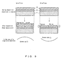
- the amount of the overall warping of the element is negligible, so that work efficiency and operability in the processes of forming an element pattern by fine processing using photolithography, bonding after the processing, dicing and the like can be improved.
- the second configuration of the dielectric thin film element of the present invention that when the thickness of the dielectric thin film is tf and the thickness of the substrate is ts, the relationships 0.2 ⁇ m ⁇ tf ⁇ 10 ⁇ m and 0.15 mm ⁇ ts ⁇ 1.5 mm are satisfied. According to this preferred example, the amount of the overall warping of the element is even less noticeable, so that the work efficiency and operability can be improved further.
- the dielectric thin film material is a piezoelectric dielectric thin film material, and the relationship ⁇ f/ ⁇ s > 1 is satisfied. According to this preferred example, it is possible to realize a dielectric thin film element having even better piezoelectric characteristics.
- the dielectric thin film material is a pyroelectric dielectric thin film material, and the relationship ⁇ f/ ⁇ s ⁇ 1 is satisfied. According to this preferred example, it is possible to realize a dielectric thin film element having even better pyloelectric characteristics.
- the dielectric thin film material includes at least lead (Pb) and titanium (Ti).
- an intermediate layer is provided between the substrate and the first electrode.
- an oxide film having a rock-salt crystal structure is used as the intermediate layer.
- the oxide film having the rock-salt crystal structure has a (100) plane orientation, a (111) plane orientation, or a (110) plane orientation.
- the oxide film having the rock-salt crystal structure is a film of at least one selected from the group consisting of magnesium oxide (MgO), nickel oxide (NiO), cobalt oxide (CoO) and manganese oxide (MnO).
- MgO magnesium oxide
- NiO nickel oxide
- CoO cobalt oxide
- MnO manganese oxide
- the dielectric thin film element of the present invention it is preferable in the second configuration of the dielectric thin film element of the present invention that at least one selected from the group consisting of platinum (Pt), palladium (Pd), iridium (Ir), gold (Au), iridium oxide (IrO 2 ), ruthenium oxide (RuO 2 ) and conductive nickel oxide (NiO) is used as a first electrode material.
- An actuator according to the present invention uses the piezoelectric dielectric thin film element of the present invention.
- An ink jet head includes an actuator, a diaphragm on which the actuator is secured, a plurality of pressure chambers accommodating an ink liquid on which the displacement of the actuator acts via the diaphragm, and the actuator of the present invention is used as the actuator.
- An ink jet recording apparatus includes an ink jet head and a recording medium transport means for transporting a recording medium in the direction approximately perpendicular to the cross direction of the ink jet head, and the ink jet head of the present invention is used as the ink jet head.
- the thermal expansion coefficient of a material constituting the actuator is ⁇ f and the thermal expansion coefficient of the material of the pressure chamber component is ⁇ s
- the material constituting the actuator and the material of the pressure chamber component are selected such that the relationship 0.8 ⁇ ⁇ f/ ⁇ s ⁇ 1.2 is satisfied, then it is possible to realize a large area ink jet head that enables high-speed and high-density printing, in which a number of nozzle holes are arranged with high density.
- FIG. 1 is a cross-sectional view showing a dielectric thin film element in a first embodiment of the present invention.
- numeral 10 denotes a dielectric thin film element.
- This dielectric thin film element 10 has a structure in which a lower electrode film made of platinum (Pt) serving as a first electrode 12, a lead zirconate titanate (PbZr 0.53 Ti 0.47 O 3 ) (hereinafter, referred to as "PZT") film (thermal expansion coefficient: about 60 ⁇ 10 -7 /K) serving as a dielectric thin film 13, and an upper electrode film made of chromium (Cr) serving as a second electrode 14 are formed in that order on a substrate 11.
- PZT lead zirconate titanate
- Cr chromium
- the above dielectric thin film element 10 was fabricated in the following manner.
- a quartz substrate was placed in a vacuum vessel as the substrate 11. After evacuation, the substrate 11 was heated and maintained at a temperature of 600°C, and a lower electrode film (Pt electrode film) having a film thickness of 250 nm and made of platinum (Pt) was formed as the first electrode 12 on the substrate 11 by RF magnetron sputtering using a 4-inch Pt target.
- the sputtering was performed for 10 minutes using argon (Ar) as a sputtering gas, maintaining the gas pressure at 1 Pa and applying a high-frequency power of 100 W.
- the substrate temperature was set to 580°C, and the dielectric thin film (PZT dielectric thin film) 14 having a film thickness of 4 ⁇ m and made of PZT was formed on the first electrode 12 by RF magnetron sputtering using a 6-inch PZT sintered compact target (with 20 mol% lead oxide (PbO) excess).
- an upper electrode film (Cr electrode film) having a film thickness of 10 nm and made of chromium (Cr) was formed as the second electrode 14 on the PZT dielectric thin film 14 by DC sputtering using a 4-inch Cr target.
- the sputtering was performed for 5 minutes using argon (Ar) as the sputtering gas, maintaining the gas pressure at 0.7 Pa and applying a power of 100 W.
- FIG. 2 shows an X-ray diffraction pattern of the PZT dielectric thin film 14 formed on the above quartz substrate via the Pt electrode film (first electrode 12). This assessment was made at the stage before forming the second electrode 14. It was found that, as shown in FIG. 2, as the Pt electrode film serving as the first electrode 12 showed (111) plane orientation, the PZT dielectric thin film 14 also showed (111) plane orientation. The diffraction angle 2 ⁇ showing a peak of the (111) plane of the PZT dielectric thin film 14 was 38.12°.
- the crystal orientation of the PZT dielectric thin film 14 is mainly the (111) plane orientation even when it is formed using the other substrates as shown above (Table 1) instead of the quartz substrate.
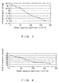
- FIG. 3 shows the results. As shown in FIG. 3, the larger the thermal expansion coefficient of the substrate is, the smaller is the diffraction angle at the (111) plane of the formed PZT dielectric thin film (and the larger is the lattice constant). This fact indicates that the lattice constant of the PZT dielectric thin film depends on the thermal expansion coefficient of the substrate.
- dielectric thin film elements were fabricated in the same manner as described above, using the various kinds of substrates with different thermal expansion coefficients as shown above (Table 1), and the relationship between the thermal expansion coefficient of the substrate and the relative dielectric constant of the formed PZT dielectric thin film was examined.
- FIG. 4 shows the results. As shown in FIG. 4, the larger the thermal expansion coefficient of the substrate is, the smaller is the relative dielectric constant of the formed PZT dielectric thin film.
- the crystal orientation of the dielectric thin film that is formed and accordingly change the film characteristics such as the electric characteristics (e.g., relative dielectric constant, coercive field, spontaneous polarization, piezoelectric constant, pyroelectric coefficient) and the optical characteristics (e.g., refractive index, electro-optic coefficient) by changing the thermal expansion coefficient of the substrate, that is, by using substrates with different thermal expansion coefficients. Therefore, it is possible to realize a dielectric thin film element whose characteristics, such as its electric characteristics, are optimized, by using a material having an optimum thermal expansion coefficient as the material of the substrate for supporting the dielectric thin film.
- the electric characteristics e.g., relative dielectric constant, coercive field, spontaneous polarization, piezoelectric constant, pyroelectric coefficient
- the optical characteristics e.g., refractive index, electro-optic coefficient
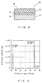
- FIG. 5 is a cross-sectional view showing a dielectric thin film element in a second embodiment of the present invention.
- dielectric thin film element 50 denotes a dielectric thin film element.
- This dielectric thin film element 50 has a structure in which an oxide film having a rock-salt crystal structure, such as a magnesium oxide (MgO) film, serving as an intermediate layer 55, a lower electrode film made of platinum (Pt) serving as a first electrode 52, a lead zirconate titanate (PbZr 0.53 Ti 0.47 O 3 ) (hereinafter, referred to as "PZT”) film (thermal expansion coefficient: about 60 ⁇ 10 -7 /K) serving as a dielectric thin film 53 and an upper electrode film made of chromium (Cr) serving as a second electrode 54 are formed in that order on a substrate 51.
- the various kinds of substrates with different thermal expansion coefficients as shown above (Table 1) are used as in the first embodiment.
- the above dielectric thin film element 50 was fabricated in the following manner.
- a Corning 7059 glass substrate was placed in a vacuum vessel as the substrate 51. After evacuation, the substrate 51 was heated and maintained at a temperature of 400°C, and the intermediate layer 55 having a film thickness of about 700 nm and made of a MgO film having a rock-salt crystal structure with a (100) plane crystalline orientation was formed on the substrate 51 by plasma MOCVD.
- magnesium acetylacetonate (Mg(C 5 H 7 O 2 ) 2 ) vaporized at a temperature of 215°C was used as a raw material gas for CVD and introduced into the vacuum vessel together with a carrier gas of inert nitrogen (N 2 ), and at the same time, an oxygen (O 2 ) gas was introduced as a reactant gas.
- the substrate 51 on which the intermediate layer 55 had been formed was placed in another vacuum vessel. After evaporation, the substrate 51 was heated and maintained at a temperature of 600°C, and the lower electrode film (Pt electrode film) having a film thickness of 250 nm and made of platinum (Pt) was formed as the first electrode 52 on the intermediate layer 55 by RF magnetron sputtering using the 4-inch Pt target. In this case, the sputtering was performed for 10 minutes using argon (Ar) as the sputtering gas, maintaining the gas pressure at 1 Pa, and applying a high-frequency power of 100 W.
- argon (Ar) argon
- the substrate temperature was set to 580 °C, and the dielectric thin film (PZT dielectric thin film) 53 having a film thickness of 4 ⁇ m and made of PZT was formed on the first electrode 52 by RF magnetron sputtering using the 6-inch PZT sintered compact target (with 20 mol% lead oxide (PbO) excess).
- the upper electrode film (Cr electrode film) having a film thickness of 10 nm and made of chromium (Cr) was formed as the second electrode 54 on the PZT dielectric thin film 53 by DC sputtering using the 4-inch Cr target.
- the sputtering was performed for 5 minutes using argon (Ar) as the sputtering gas, maintaining the gas pressure at 0.7 Pa and applying a power of 100 W.
- FIG. 6 shows an X-ray diffraction pattern of the PZT dielectric thin film 53 formed on the above Corning 7059 glass substrate via the MgO film (intermediate layer 55) having the (100) plane orientation and the Pt electrode film (first electrode 52).
- This assessment was made at the stage before forming the second electrode 54. It was found that, as shown in FIG. 6, as the Pt electrode film serving as the first electrode 52 showed (100) plane orientation, the PZT dielectric thin film 53 showed (001) plane orientation.
- the diffraction angles 2 ⁇ showing the peaks of a (001) plane and a (002) plane of the PZT dielectric thin film 53 were 21.73° and 44.22°, respectively.
- the crystal orientation of the PZT dielectric thin film 53 that is formed via the MgO film (intermediate layer 55) is mainly the (001) plane orientation even when it is formed using the other substrates as shown above (Table 1) instead of the Corning 7059 glass substrate.
- FIG. 7 shows the results. As shown in FIG. 7, the larger the thermal expansion coefficient of the substrate is, the smaller is the diffraction angle at the (002) plane of the formed PZT dielectric thin film (and the larger is the lattice constant). This fact indicates that, as in the first embodiment, the lattice constant of the PZT dielectric thin film depends on the thermal expansion coefficient of the substrate.
- dielectric thin film elements were fabricated in the same manner as described above, using the various kinds of substrates with different thermal expansion coefficients as shown above (Table 1), and the relationship between the thermal expansion coefficient of the substrate and the relative dielectric constant of the formed PZT dielectric thin film was examined.
- FIG. 8 shows the results. As shown in FIG. 8, the larger the thermal expansion coefficient of the substrate is, the smaller is the relative dielectric constant of the formed PZT dielectric thin film, as in the first embodiment.
- the crystal orientation of the dielectric thin film that is formed and accordingly change the film characteristics such as the electric characteristics (e.g., relative dielectric constant, coercive field, spontaneous polarization, piezoelectric constant, pyroelectric coefficient) and the optical characteristics (e.g., refractive index, electro-optic coefficient) by changing the thermal expansion coefficient of the substrate, that is, by using substrates with different thermal expansion coefficients.
- the electric characteristics e.g., relative dielectric constant, coercive field, spontaneous polarization, piezoelectric constant, pyroelectric coefficient
- the optical characteristics e.g., refractive index, electro-optic coefficient
- the oxide film having the rock-salt crystal structure used as the intermediate layer 55 showed (111) plane orientation or (110) plane orientation
- the formed PZT dielectric thin film also showed (111) plane orientation or (110) plane orientation, respectively, and the crystal parameters such as the lattice constant and the film characteristics such as the relative dielectric constant of the dielectric thin film with respect to the thermal expansion coefficient of the substrate showed exactly the same tendencies.
- the thickness of the intermediate layer is negligible compared to that of the substrate and, when the thermal expansion coefficient of the dielectric thin film material is ⁇ f and the thermal expansion coefficient of the substrate is ⁇ s, if the relationship 0.8 ⁇ ⁇ f/ ⁇ s ⁇ 1.2 is satisfied, then the amount of the overall warping of the element is negligible, so that the work efficiency and operability in the processes of forming an element pattern by fine processing using photolithography, bonding after the processing, dicing and the like can be improved. Therefore, large numbers of dielectric thin film elements can be produced at low prices by using a substrate having a large surface area.
- a pyroelectric dielectric thin film element 50 of this embodiment has a structure in which an oxide film having a rock-salt crystal structure, such as a magnesium oxide (MgO) film, serving as an intermediate layer 55, a lower electrode film made of platinum (Pt) serving as a first electrode 52, a lead lanthanum titanate (Pb 0.9 La 0.1 Ti 0.975 O 3 ) (hereinafter, referred to as "PLT") film (thermal expansion coefficient: about 30 ⁇ 10 -7 K) serving as a dielectric thin film 53 and an upper electrode film made of nichrome (NiCr) serving as a second electrode 54 are formed in that order on a substrate 51.
- PKT lead lanthanum titanate
- NiCr nichrome
- the above pyroelectric dielectric thin film element 50 was fabricated in the following manner.
- a SUS304 substrate was placed in a vacuum vessel as the substrate 51. After evacuation, the substrate 51 was heated and maintained at a temperature of 400°C as in the second embodiment 2, and the intermediate layer 55 having a film thickness of about 700 nm and made of the MgO film having the rock-salt crystal structure with the (100) plane crystalline orientation was formed on the substrate 51 by plasma MOCVD.
- a magnesium acetylacetonate gas (Mg(C 5 H 7 O 2 ) 2 ) vaporized at a temperature of 215°C was used as the raw material gas for CVD and introduced into the vacuum vessel together with the carrier gas of inert nitrogen (N 2 ), and at the same time, oxygen (O 2 ) gas was introduced as the reactant gas.
- the substrate 51 on which the intermediate layer 55 had been formed was placed in another vacuum vessel. After evacuation, the substrate 51 was heated and maintained at a temperature of 600°C, and the lower electrode film (Pt electrode film) having a film thickness of 250 nm and made of platinum (Pt) was formed as the first electrode 52 on the intermediate layer 55 by RF magnetron sputtering using the 4-inch Pt target. In this case, the sputtering was performed for 10 minutes using argon (Ar) as the sputtering gas, maintaining the gas pressure at 1 Pa and applying a high-frequency power of 100 W.
- argon (Ar) argon
- the substrate temperature was set to 560°C, and the dielectric thin film (PLT dielectric thin film) 53 having a film thickness of 3 ⁇ m and made of PLT was formed on the first electrode 52 by RF magnetron sputtering using a 6-inch PLT sintered compact target (with 20 mol% lead oxide (PbO) excess).
- the upper electrode film (NiCr electrode film) having a film thickness of 10 nm and made of nichrome (NiCr) was formed as the second electrode 54 on the PLT dielectric thin film 53 by DC sputtering using a 4-inch NiCr target.
- the sputtering was performed for 5 minutes using argon (Ar) as the sputtering gas, maintaining the gas pressure at 0.7 Pa and applying a power of 100 W.
- the crystal orientation of the PLT dielectric thin film 53 that is formed via the MgO film (intermediate layer 55) is mainly a (001) plane orientation even when it is formed using the other substrates as shown above (Table 1) instead of the SUS304 substrate.
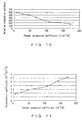
- FIG. 10 shows the results. As shown in FIG. 10, the larger the thermal expansion coefficient of the substrate is, the smaller is the relative dielectric constant of the formed PLT dielectric thin film, as in the second embodiment.
- FIG. 11 shows the results. As shown in FIG. 11, the larger the thermal expansion coefficient of the substrate is, the larger is the pyroelectric coefficient ⁇ of the PLT dielectric thin film.
- the pyroelectric performance can be represented in a simple manner by the ratio ⁇ / ⁇ of the pyroelectric coefficient ⁇ to the relative dielectric constant ⁇ . Therefore, based on the above results, it can be seen that the higher the thermal expansion coefficient of the used substrate is, the better is the performance of the pyroelectric infrared sensor. That is to say, when the thermal expansion coefficient of the dielectric thin film material is ⁇ f and the thermal expansion coefficient of the substrate is ⁇ s, if the relationship ⁇ f/ ⁇ s ⁇ 1 is satisfied, it is possible to realize a pyroelectric dielectric thin film element having a good performance.
- the oxide film having the rock-salt crystal structure used as the intermediate layer 55 had the (111) plane orientation or the (110) plane orientation
- the formed PLT dielectric thin film also showed the (111) plane orientation or the (110) plane orientation, respectively, and the film characteristics such as the relative dielectric constant and the pyroelectric performance of the dielectric thin film with respect to the thermal expansion coefficient of the substrate showed exactly the same tendencies.
- the thickness of the intermediate layer is negligible compared to that of the substrate and, when the thermal expansion coefficient of the dielectric thin film material is ⁇ f and the thermal expansion coefficient of the substrate is ⁇ s, if the relationship 0.8 ⁇ ⁇ f/ ⁇ s ⁇ 1.2 is satisfied, the amount of the overall warping of the element is negligible, so that the work efficiency and operability in the processes of forming an element pattern by fine processing using photolithography, bonding after the processing, dicing and the like can be improved. Therefore, large numbers of large area dielectric thin film elements such as dielectric thin film elements and infrared imaging elements can be produced at low prices by using a substrate having a large surface area.
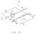
- FIG. 12 is a schematic perspective view showing the overall configuration of an ink jet recording apparatus in a fourth embodiment of the present invention.
- the ink jet recording apparatus 100 of this embodiment is provided with an ink jet head 101 for performing recordings by utilizing the piezoelectric effect of a piezoelectric dielectric thin film, and can perform the recordings on a recording medium 102 such as a paper by letting ink droplets ejected from the ink jet head 101 land on the recording medium 102.
- the ink jet head 101 is mounted on a carriage 104 that is slidably attached to a carriage shaft 103 arranged along the principal scanning direction (X direction in FIG. 12).
- the carriage 104 moves back and forth along the carriage shaft 103, and thus the ink jet head 101 moves back and forth in the principal scanning direction X. Furthermore, the ink jet recording apparatus 100 is provided with a plurality of rollers (recording medium transport means) 105 for moving the recording medium 102 in the secondary scanning direction Y, which is approximately perpendicular to the cross direction of the ink jet head 101 (i.e., principal scanning direction X).
- a plurality of rollers (recording medium transport means) 105 for moving the recording medium 102 in the secondary scanning direction Y, which is approximately perpendicular to the cross direction of the ink jet head 101 (i.e., principal scanning direction X).
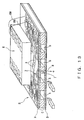
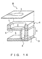
- FIG. 13 is a schematic perspective view showing the overall configuration of the ink jet head in the fourth embodiment of the present invention and FIG. 14 is a partially cutaway exploded perspective view showing a configuration of its relevant part.
- letter A denotes a pressure chamber component that is formed by processing, for example, a silicon (Si) substrate, and a pressure chamber aperture portion 1 is formed in this pressure chamber component A.
- Letter B denotes an actuator constituted by the dielectric thin film element of the present invention that is arranged so as to cover the upper aperture side of the pressure chamber aperture portion 1
- letter C denotes an ink liquid passage component that is arranged so as to cover the lower aperture side of the pressure chamber aperture portion 1.
- the pressure chamber aperture portion 1 of the pressure chamber component A is partitioned by the actuator B and the ink liquid passage component C that are positioned above and below thereof, and thus a pressure chamber 2 is formed.
- the actuator B an individual electrode 3 is arranged above the pressure chamber 2.
- a number of pressure chambers 2 and individual electrodes 3 are arranged in a staggered pattern.
- a common liquid chamber 5 that is shared by the pressure chambers 2, a supply port 6 for linking this common liquid chamber 5 with the pressure chamber 2, and an ink passage 7 through which the ink liquid within the pressure chamber 2 flows out are formed, aligned in the ink liquid supply direction.
- Letter D denotes a nozzle plate, and a nozzle hole 8 linked to the ink passage 7 is bored in this nozzle plate D.
- letter E denotes an IC chip and this IC chip E supplies voltage to a plurality of individual electrodes 3 via bonding wires BW.
- the dielectric thin film element constituting the actuator B it is possible to control the performance of the dielectric thin film element constituting the actuator B by selecting the material of the pressure chamber component A, which is formed by processing the substrate, taking into account its thermal expansion coefficient.
- the thermal expansion coefficient of the material constituting the actuator B (dielectric thin film material)
- the thermal expansion coefficient of the material of the pressure chamber component A is ⁇ s
- the material constituting the actuator B and the material of the pressure chamber component A are selected such that the relationship ⁇ f/ ⁇ s > 1 is satisfied, then it is possible to realize an ink jet head having a dielectric thin film element with better piezoelectric characteristics (in this case, print characteristics).
- the material constituting the actuator B and the material of the pressure chamber component A are selected such that the above ⁇ f and ⁇ s satisfy the relationship 0.8 ⁇ ⁇ f/ ⁇ s ⁇ 1.2, then it is possible to realize a large area ink jet head that enables high-speed and high-density printing, in which a number of nozzle holes are arranged with high density.
- the present invention can provide a dielectric thin film element provided with a dielectric thin film whose film characteristics such as the relative dielectric constant can be changed considerably, by selecting a substrate material in consideration of the thermal expansion coefficient, so that it can be used for piezoelectric elements, infrared sensors, optical switches, memory elements and the like which require the element characteristics to be controlled and optimized with high yield rate.
Landscapes
- Engineering & Computer Science (AREA)
- Manufacturing & Machinery (AREA)
- Chemical & Material Sciences (AREA)
- Ceramic Engineering (AREA)
- Photometry And Measurement Of Optical Pulse Characteristics (AREA)
- Formation Of Insulating Films (AREA)
- Particle Formation And Scattering Control In Inkjet Printers (AREA)
Applications Claiming Priority (3)
| Application Number | Priority Date | Filing Date | Title |
|---|---|---|---|
| JP2000293803 | 2000-09-27 | ||
| JP2000293803 | 2000-09-27 | ||
| PCT/JP2001/008402 WO2002027809A1 (en) | 2000-09-27 | 2001-09-26 | Dielectric thin film element, actuator comprising it, ink jet head, and ink jet recorder. |
Publications (1)
| Publication Number | Publication Date |
|---|---|
| EP1324401A1 true EP1324401A1 (de) | 2003-07-02 |
Family
ID=18776526
Family Applications (1)
| Application Number | Title | Priority Date | Filing Date |
|---|---|---|---|
| EP01970233A Withdrawn EP1324401A1 (de) | 2000-09-27 | 2001-09-26 | Dielektrisches dünnfilmelement, stellelement damit, ink jet-kopf und ink jet-recorder |
Country Status (7)
| Country | Link |
|---|---|
| US (1) | US20030189241A1 (de) |
| EP (1) | EP1324401A1 (de) |
| JP (1) | JPWO2002027809A1 (de) |
| KR (1) | KR100532736B1 (de) |
| CN (1) | CN1483225A (de) |
| AU (1) | AU2001290283A1 (de) |
| WO (1) | WO2002027809A1 (de) |
Cited By (1)
| Publication number | Priority date | Publication date | Assignee | Title |
|---|---|---|---|---|
| WO2003023873A3 (de) * | 2001-09-07 | 2003-11-27 | Drei S Werk Praez Swerkzeuge G | Flacher aktor oder sensor mit interner vorspannung |
Families Citing this family (16)
| Publication number | Priority date | Publication date | Assignee | Title |
|---|---|---|---|---|
| JP4513252B2 (ja) * | 2002-10-25 | 2010-07-28 | パナソニック株式会社 | 圧電体薄膜素子およびそれを用いたアクチュエータ、インクジェットヘッドならびにインクジェット記録装置 |
| JP2005136115A (ja) * | 2003-10-30 | 2005-05-26 | Tdk Corp | 電子デバイス及びその製造方法 |
| JP5089860B2 (ja) * | 2004-12-03 | 2012-12-05 | 富士フイルム株式会社 | 圧電アクチュエータ及び液体吐出ヘッド |
| JP2006245247A (ja) * | 2005-03-02 | 2006-09-14 | Seiko Epson Corp | 圧電素子及びその製造方法、液体噴射ヘッド及びその製造方法並びに液体噴射装置 |
| JP4543985B2 (ja) * | 2005-03-24 | 2010-09-15 | セイコーエプソン株式会社 | ニオブ酸チタン酸ジルコン酸鉛積層体 |
| JP5391395B2 (ja) * | 2007-10-15 | 2014-01-15 | 日立金属株式会社 | 圧電薄膜付き基板及び圧電素子 |
| US7896479B2 (en) * | 2008-04-30 | 2011-03-01 | Seiko Epson Corporation | Liquid jet head and a piezoelectric element |
| DE102008055123B3 (de) * | 2008-12-23 | 2010-07-22 | Robert Bosch Gmbh | Ultraschallwandler zum Einsatz in einem fluiden Medium |
| IN2014DN09377A (de) * | 2012-04-10 | 2015-07-17 | Corinthian Ophthalmic Inc | |
| US9539604B2 (en) | 2012-05-15 | 2017-01-10 | Eyenovia, Inc. | Ejector devices, methods, drivers, and circuits therefor |
| US9136820B2 (en) | 2012-07-31 | 2015-09-15 | Tdk Corporation | Piezoelectric device |
| WO2014088691A1 (en) * | 2012-12-03 | 2014-06-12 | Advanced Technology Materials Inc. | IN-SITU OXIDIZED NiO AS ELECTRODE SURFACE FOR HIGH k MIM DEVICE |
| US9016836B2 (en) | 2013-05-14 | 2015-04-28 | Stmicroelectronics, Inc. | Ink jet printhead with polarity-changing driver for thermal resistors |
| US9016837B2 (en) | 2013-05-14 | 2015-04-28 | Stmicroelectronics, Inc. | Ink jet printhead device with compressive stressed dielectric layer |
| JP6467258B2 (ja) * | 2015-03-20 | 2019-02-06 | 日本碍子株式会社 | 接合体、ハニカム構造体及び接合体の製造方法 |
| US11737280B2 (en) * | 2021-03-05 | 2023-08-22 | Taiwan Semiconductor Manufacturing Company, Ltd. | Wakeup free approach to improve the ferroelectricity of FeRAM using a stressor layer |
Family Cites Families (12)
| Publication number | Priority date | Publication date | Assignee | Title |
|---|---|---|---|---|
| JP2532410B2 (ja) * | 1986-11-14 | 1996-09-11 | 松下電器産業株式会社 | 誘電体薄膜素子 |
| JP3419008B2 (ja) * | 1992-12-24 | 2003-06-23 | 株式会社村田製作所 | 圧電素子の製造方法 |
| JPH06196648A (ja) * | 1992-12-25 | 1994-07-15 | Fuji Xerox Co Ltd | 配向性強誘電体薄膜素子 |
| US5866238A (en) * | 1994-05-05 | 1999-02-02 | Minolta Co., Ltd. | Ferroelectric thin film device and its process |
| JPH07300397A (ja) * | 1994-05-10 | 1995-11-14 | Matsushita Electric Ind Co Ltd | 強誘電体薄膜素子およびその製造方法 |
| JPH0867599A (ja) * | 1994-08-30 | 1996-03-12 | Sanyo Electric Co Ltd | 強誘電体薄膜の製造方法 |
| EP0747976B1 (de) * | 1994-12-27 | 2000-06-07 | Seiko Epson Corporation | Piezoelektrische dünnschichtanordnung, verfahren zur herstellung derselben und einen diese anordnung enthaltenden tintenstrahldruckkopf |
| JPH08186182A (ja) * | 1994-12-28 | 1996-07-16 | Matsushita Electric Ind Co Ltd | 強誘電体薄膜素子 |
| JPH10154834A (ja) * | 1996-11-21 | 1998-06-09 | Matsushita Electric Ind Co Ltd | 強誘電体素子およびその製造方法 |
| US5719417A (en) * | 1996-11-27 | 1998-02-17 | Advanced Technology Materials, Inc. | Ferroelectric integrated circuit structure |
| US6376090B1 (en) * | 1998-09-25 | 2002-04-23 | Sharp Kabushiki Kaisha | Method for manufacturing a substrate with an oxide ferroelectric thin film formed thereon and a substrate with an oxide ferroelectric thin film formed thereon |
| JP2000196157A (ja) * | 1998-12-28 | 2000-07-14 | Ube Ind Ltd | 圧電体素子、及び圧電体素子の製造方法、並びにこの圧電体素子を用いたインクジェットヘッド、インクジェットプリンタ |
-
2001
- 2001-09-26 EP EP01970233A patent/EP1324401A1/de not_active Withdrawn
- 2001-09-26 KR KR10-2003-7004432A patent/KR100532736B1/ko not_active Expired - Fee Related
- 2001-09-26 WO PCT/JP2001/008402 patent/WO2002027809A1/ja not_active Ceased
- 2001-09-26 JP JP2002531503A patent/JPWO2002027809A1/ja not_active Withdrawn
- 2001-09-26 CN CNA018164129A patent/CN1483225A/zh active Pending
- 2001-09-26 AU AU2001290283A patent/AU2001290283A1/en not_active Abandoned
- 2001-09-26 US US10/380,712 patent/US20030189241A1/en not_active Abandoned
Non-Patent Citations (1)
| Title |
|---|
| See references of WO0227809A1 * |
Cited By (1)
| Publication number | Priority date | Publication date | Assignee | Title |
|---|---|---|---|---|
| WO2003023873A3 (de) * | 2001-09-07 | 2003-11-27 | Drei S Werk Praez Swerkzeuge G | Flacher aktor oder sensor mit interner vorspannung |
Also Published As
| Publication number | Publication date |
|---|---|
| US20030189241A1 (en) | 2003-10-09 |
| WO2002027809A1 (en) | 2002-04-04 |
| KR100532736B1 (ko) | 2005-12-01 |
| JPWO2002027809A1 (ja) | 2004-02-05 |
| AU2001290283A1 (en) | 2002-04-08 |
| CN1483225A (zh) | 2004-03-17 |
| KR20030048413A (ko) | 2003-06-19 |
Similar Documents
| Publication | Publication Date | Title |
|---|---|---|
| US20030189241A1 (en) | Dielectric thin film element, actuator comprising it, ink jet head, and ink jet recorder | |
| US7279825B2 (en) | Dielectric thin film element, piezoelectric actuator and liquid discharge head, and method for manufacturing the same | |
| KR100651046B1 (ko) | 유전체막 구조체, 유전체막 구조체를 사용하는 압전액추에이터 및 잉크젯 헤드 | |
| EP1588437B1 (de) | Piezoelektrisches element | |
| EP2044245B1 (de) | Piezoelektrische substanz, piezoelektrisches element und flüssigkeitsausstosskopf sowie flüssigkeitsausstossvorrichtung mit dem piezoelektrischen element | |
| KR100485551B1 (ko) | 압전 소자 구조와 액체 분사 기록 헤드, 및 그 제조 방법 | |
| US7845767B2 (en) | Piezoelectric device, method of actuating the same, piezoelectric apparatus, and liquid discharge apparatus | |
| US7033521B2 (en) | Piezoelectric actuator, ink jet head, and discharge apparatus | |
| US20080302658A1 (en) | Oxide body, piezoelectric device, and liquid discharge device | |
| US7591543B2 (en) | Piezoelectric member, piezoelectric member element, liquid discharge head in use thereof, liquid discharge apparatus and method of manufacturing piezoelectric member | |
| EP0991130B1 (de) | Piezoelektrisches gerät, tintenstrahldruckkopf, verfahren zum herstellen und drucker | |
| US20040155559A1 (en) | Ferroelectric thin film element, piezoelectric actuator and liquid discharge head | |
| US20100079555A1 (en) | Lead-containing perovskite-type oxide film and method of producing the same, piezoelectric device using a lead-containing perovskite-type oxide film, as well as liquid ejecting apparatus using a piezoelectric device | |
| US6739703B2 (en) | Piezoelectric actuator and liquid discharge head | |
| US20090295876A1 (en) | Ferroelectric oxide structure, method for producing the structure, and liquid-discharge apparatus | |
| US7528530B2 (en) | Piezoelectric substance, piezoelectric substance element, liquid discharge head, liquid discharge device and method for producing piezoelectric substance | |
| US20040051763A1 (en) | Piezoelectric thin film element, actuator, ink-jet head and ink-jet recording apparatus therefor | |
| US6943485B2 (en) | Piezoelectric actuator, liquid jetting head and liquid jetting device using the same | |
| JP2007243200A (ja) | 圧電体デバイス、液体吐出ヘッド、強誘電体デバイス及び電子機器並びにこれらの製造方法 | |
| US7193756B2 (en) | Piezoelectric element, method for fabricating the same, inkjet head, method for fabricating the same, and inkjet recording apparatus | |
| US7830073B2 (en) | Perovskite oxide, electric element, piezoelectric actuator and liquid discharge system | |
| JP4513252B2 (ja) | 圧電体薄膜素子およびそれを用いたアクチュエータ、インクジェットヘッドならびにインクジェット記録装置 | |
| JP2004179642A (ja) | 圧電体デバイス、液体吐出ヘッド、強誘電体デバイス及び電子機器並びにこれらの製造方法 | |
| JP2007154275A (ja) | 成膜方法および圧電体薄膜 |
Legal Events
| Date | Code | Title | Description |
|---|---|---|---|
| PUAI | Public reference made under article 153(3) epc to a published international application that has entered the european phase |
Free format text: ORIGINAL CODE: 0009012 |
|
| 17P | Request for examination filed |
Effective date: 20030313 |
|
| AK | Designated contracting states |
Designated state(s): AT BE CH CY DE DK ES FI FR GB GR IE IT LI LU MC NL PT SE TR |
|
| AX | Request for extension of the european patent |
Extension state: AL LT LV MK RO SI |
|
| RBV | Designated contracting states (corrected) |
Designated state(s): DE FR GB IT NL |
|
| STAA | Information on the status of an ep patent application or granted ep patent |
Free format text: STATUS: THE APPLICATION HAS BEEN WITHDRAWN |
|
| 18W | Application withdrawn |
Effective date: 20061115 |