EP1326302A2 - Fraktale Antenne in integrierter Schaltung für ein Hörgerät - Google Patents
Fraktale Antenne in integrierter Schaltung für ein Hörgerät Download PDFInfo
- Publication number
- EP1326302A2 EP1326302A2 EP02258281A EP02258281A EP1326302A2 EP 1326302 A2 EP1326302 A2 EP 1326302A2 EP 02258281 A EP02258281 A EP 02258281A EP 02258281 A EP02258281 A EP 02258281A EP 1326302 A2 EP1326302 A2 EP 1326302A2
- Authority
- EP
- European Patent Office
- Prior art keywords
- hearing aid
- conductive pattern
- fractal
- signal
- antenna
- Prior art date
- Legal status (The legal status is an assumption and is not a legal conclusion. Google has not performed a legal analysis and makes no representation as to the accuracy of the status listed.)
- Withdrawn
Links
Images





Classifications
-
- H—ELECTRICITY
- H01—ELECTRIC ELEMENTS
- H01Q—ANTENNAS, i.e. RADIO AERIALS
- H01Q1/00—Details of, or arrangements associated with, antennas
- H01Q1/36—Structural form of radiating elements, e.g. cone, spiral, umbrella; Particular materials used therewith
- H01Q1/38—Structural form of radiating elements, e.g. cone, spiral, umbrella; Particular materials used therewith formed by a conductive layer on an insulating support
-
- H—ELECTRICITY
- H01—ELECTRIC ELEMENTS
- H01Q—ANTENNAS, i.e. RADIO AERIALS
- H01Q1/00—Details of, or arrangements associated with, antennas
- H01Q1/27—Adaptation for use in or on movable bodies
- H01Q1/273—Adaptation for carrying or wearing by persons or animals
-
- H—ELECTRICITY
- H04—ELECTRIC COMMUNICATION TECHNIQUE
- H04R—LOUDSPEAKERS, MICROPHONES, GRAMOPHONE PICK-UPS OR LIKE ACOUSTIC ELECTROMECHANICAL TRANSDUCERS; ELECTRIC HEARING AIDS; PUBLIC ADDRESS SYSTEMS
- H04R2225/00—Details of deaf aids covered by H04R25/00, not provided for in any of its subgroups
- H04R2225/51—Aspects of antennas or their circuitry in or for hearing aids
Definitions
- the invention relates to fractal antennas, and more particularly a fractal antenna in an integrated circuit.
- Programmable hearing aids allow precise adjustment of the specific parameters of hearing aid operation so as to achieve reasonably good operation personalized for the user.
- Hearing aids have traditionally been programmed with a multi-wire interface, including a physical connection to a device worn on the body that incorporates a wired link to the hearing aid programmer, e.g. a multi-wire interface directly between the programmer and the hearing aid.
- a wire interface requires the hearing aid to incorporate a connector, or multiple connectors, into its structure for the programming cable, which can be cumbersome and complicated for the user.
- Typical programming interfaces use serial data transmission employing two to four electrical connections located on the hearing aid device. Alternately, newer connection schemes use the battery terminals on the hearing aid device to supply power and transmit data to the hearing aid. This approach, however, sometimes requires additional battery contacts depending on the nature of the serial data interface. These data transmission methods require special programming cables and small sized connectors that are fragile and costly to manufacture. In addition, due to the physically small size of hearing aids, reliable wire connections to the hearing aid device from the programming device can be difficult to achieve.
- Wireless programming methods such as infrared and ultrasonic links, have been used in the past in place of a multi-wire programming interface, but generally require relatively complex circuitry and introduce additional limitations to the device and programming capabilities.
- Infrared and ultrasonic links generally experience high rates of power consumption and are susceptible to interference and undesirable directional characteristics.
- an improved wireless programming interface would greatly increase the ease and reliability of programming a hearing aid.
- a programmable hearing aid configured to transmit and/or receive a signal to and/or from a programming device, comprises a semiconductor substrate, a conductive pattern, disposed on the semiconductor substrate so as to transmit and/or receive a signal to and/or from the programming device, wherein the conductive pattern comprises a plurality of fractal elements of different scales and orientations.
- the programmable hearing aid further comprises transmit and/or receive circuitry, disposed on the semiconductor substrate, coupled to the conductive pattern and configured to receive and process a signal from the conductive pattern, and/or process a signal to be transmitted to the conductive pattern.
- the plurality of fractal elements can be of a generally + shaped geometry.
- a method of programming a plurality of parameters in a wireless hearing aid comprises receiving a programming signal at a fractal antenna in the hearing aid, wherein the fractal antenna comprises a conductive pattern disposed on a substrate, and wherein the conductive pattern comprises a plurality of fractal elements, repeated in multiple scales and orientations.
- the method further comprises processing the programming signal in a receiver circuit in the hearing aid, thereby producing a processed programming signal, the receiver circuit coupled to said fractal antenna, and modifying at least one parameter in the hearing aid with at least one of the parameters from the processed programming signal.
- a fractal antenna comprises a plurality of fractal elements, wherein each fractal element comprises a generally +-shaped geometry, and the plurality of fractal elements are repeated in a plurality of scales and orientations.
- the fractal antenna can be disposed on a semiconductor substrate as a conductive pattern, and can be incorporated in a hearing aid device.
- An integrated circuit comprises a semiconductor substrate, a conductive pattern, defining a plurality of fractal elements of a generally + shaped geometry of different dimensions, disposed on said semiconductor substrate.
- the integrated circuit may further comprise a receiver circuit, coupled to the conductive pattern and configured to receive a signal from the conductive pattern.
- the integrated circuit may also further comprise a transmit circuit, coupled to the conductive pattern and configured to transmit a signal to the conductive pattern.
- Figure 1 is an exemplary illustration of a hearing aid device.
- FIG. 2 is an illustration of a fractal antenna structure, referred to herein as a Pollard antenna structure.
- FIG. 3 is a magnified illustration of the Pollard antenna of Figure 1.
- FIG. 4 is an illustration of an alternative Pollard antenna structure.
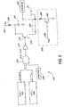
- Figure 5 is an exemplary schematic diagram of a signal transmission circuit.
- Figure 6 is an exemplary illustration of a signal transmission circuit disposed on a substrate for a fractal antenna.
- Figure 7 is a substrate layer diagram, corresponding to the signal transmission circuit illustrated in Figure 6.
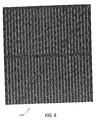
- Figure 8 is more detailed illustration of one embodiment of a capacitor for incorporation in the signal transmission circuit of Figure 6.
- Figure 9 is a more detailed illustration of one embodiment of a signal transmission line for incorporation in the signal transmission circuit of Figure 6.
- Wireless data transmissions typically include the use of signal transmission antennas, which can vary in size and shape depending on the application.
- An arbitrary reduction in the size of a conventional antenna can result in a large reactance and degradation in the performance of the antenna.
- a small sized loop antenna, or short dipole requires significant space due to its performance dependence upon the physical area of the antenna. Therefore, due to the small size of hearing aids, the use of conventional signal transmission antennas does not readily apply.
- a conductive pattern can be deposited on a substrate to form a plurality of fractal elements, resulting in a resonator, or fractal antenna.
- the plurality of fractal elements can be of different dimensional sizes and in a number of spatial orientations.
- a fractal antenna 20 can be incorporated in a hearing aid 10 to facilitate communications with a programming box 30. It will be appreciated that the antenna 20 can be used to transmit and/or receive signals from devices other than the programming box 30, such as a wireless telephone.
- the programming box 30 can communicate hearing aid parameters to the hearing aid device 10, and can receive information from the hearing aid device 10.
- the fractal antenna 20 can be implemented as a conductive pattern, disposed on a substrate, comprising a number of fractal elements repeated in multiple orientations and scales.
- the fractal antenna 20 can be configured to receive and/or transmit signals to and/or from the programming box 30.
- the hearing aid 10 can appropriately have receive and/or transmit circuitry (not shown), so as to process a received signal, or process a signal for transmission.
- Fractals have been used to model many environmental phenomenon, such as trees and lightning, and common references in the art are authored by Hans Lauwerier, and Benoit Mandlebrot. Fractals consist of similar or identical elements repeated in different orientations, positions, and degrees of magnification, typically in an interconnected order. Most fractals have an infinite complexity and detail, thus the complexity and detail of the fractals remain no matter how far an observer magnifies the fractal object. The combination of infinite complexity and detail, in addition to the self-similarity inherent to fractal geometry, makes it possible to construct very small sized antennas with fractal structures, which can operate at high efficiency at multiple frequencies. Although a fractal is infinite by definition, a practical fractal is referred to herein where the multitude and level of scales at which the fractal is repeated can change as implementation technology permits.
- a fractal antenna is a pattern of conductive or semi-conductive material in two or three dimensions having at least one geometric feature that is repeated on different scales, different positions, and/or in different orientations.
- the repeated feature is a "+", "x", or cross.
- a fractal antenna structure can produce a directive radiation pattern at a given frequency, and can therefore be useful in a wireless hearing aid communication system due to the structure's size reduction capabilities.
- the fractal antenna 20 is appropriate for a low energy, low power system such as the hearing aid 10 due to both size constraints of the device and the prospect of matching the load impedance by selecting a frequency in a range such as about 1 MHz to 1 GHz.
- fractal antenna structures Very few fractal patterns, such as Hilbert curves and the Sierpenski gasket, have been implemented as fractal antenna structures.
- the use of fractals in an antenna geometry in addition to being simple and self-similar, can allow a plane to be filled with different size iterations of similar geometry, and such properties can be exploited to form a reduced size resonant antenna.
- FIG. 2 illustrates a fractal antenna structure, referred to herein as a Pollard structure.
- the Pollard antenna structure consists of a fractal geometry similar to an X-shape, or cross, repeated in multiple orientations and scales to form, in one embodiment, a structure such as that illustrated in Figure 2.
- a specific area of the antenna in Figure 2 such as area 60
- the X-shape, + shape, or cross geometry is maintained, but on a smaller scale, as shown in Figure 3.
- Fractal antennas can be extensively reduced in size while maintaining resonant characteristics which correspond to much larger antennas, including deposition on something as small as an integrated circuit substrate.
- the fractal Antenna of Figure 2 can be formed by depositing connected substantially linear segments of conductive material on a substrate in the pattern illustrated in Figure 2.
- An alternate fractal antenna can be formed by depositing linear segments of conductive material on a substrate in a pattern defined by the opposed edges of the linear segments shown in Figure 2. This embodiment is illustrated in Figure 4.
- the antenna pattern of Figure 4 can be formed by depositing thick linear segments in the solid pattern of Figure 2, and then etching away the central portion of the thick linear segments, thereby leaving behind an outline of conductive material defined by the perimeter of the linear pattern shown in Figure 2.
- the Pollard antenna design can be reduced from about 1.4mm on a side, down to about 0.4mm on a side for incorporation in small electronic devices, such as the hearing aid illustrated in Figure 1.
- a fractal antenna in the hearing aid device 10 can allow the device to communicate, or be programmed by a remote device without incorporating additional connectors onto the device.
- Such receive and transmit capabilities can allow the device to be programmed without wired connections, or to receive specialized signals in environments modified for hearing aid device users.
- hearing aid users Many performance and concert venues have recently been constructed or updated to assist hearing aid users in such environments, and cellular phones can be adapted to function in combination with a hearing aid device. It would be beneficial for hearing aid users to have the capability to utilize such enhancements and adaptations without having to adjust settings on their individual devices, or without having to use an additional external device and connection in such an environment. Such capabilities can be realized by the incorporation of the fractal antenna 20 in the hearing aid 10 of Figure 1.
- the hearing aid 10 can receive signals from the modified environment or communication device at the fractal antenna 20, without having to use an additional aiding device or wire connection.
- a transmitter can also be used as a receiver to assist in determining antenna characteristics.
- the majority of the following description of a fractal antenna and corresponding circuitry will pertain to transmission capabilities of the device, however, it will be appreciated that such design approaches are applicable to receive capabilities and the device may be optimized for either or both functions.
- FIG. 5 is a schematic diagram of an exemplary signal transmission circuit 200 for use with a fractal antenna, such as the Pollard antennas illustrated in Figures 2-4.
- the circuit can be implemented in the hearing aid 10 of Figure 1, including the fractal antenna 20.
- the circuit 200 comprises a first voltage controlled oscillator (VCO1) 204 and second voltage controlled oscillator (VCO2) 206, wherein the oscillation frequencies of such signal sources 204, 206 can be set by applying a DC voltage.
- the voltage controlled oscillators 204, 206 can operate at a 50% duty cycle at frequencies of about 1 KHz to about 1 GHz.
- a logic gate 210 in this case an AND gate, receives output signals from the pulse train source 204, the envelope source 206, and a control input 208. Thereby, the AND gate 210 transmits one or a series of pulse trains from the first voltage controlled oscillator 204 when the control input 208 is triggered.
- a signal from the output of the logic gate 210 is received at a buffer 214, or network of buffers, etc. More particularly, the buffer 214 can be implemented as a ladder structure, wherein each parallel rung is a buffer in series with a resistive element.
- the output of the buffer 210 is connected to a switch, which is implemented in this embodiment as a PMOS transistor 218, wherein the output of the buffer 210 is connected to a gate terminal 219 of the PMOS transistor 218.
- the source terminal of the PMOS transistor 218 is coupled to a capacitor 220, which receives a charging voltage from a source V cc 224 through a resistor 226.
- a first end of a transmission line 225 can be connected to the drain terminal of the transistor 218, and a second end of the transmission line 225 can be connected directly to the fractal antenna 20.
- the capacitor 220 is allowed to charge from the voltage source V cc 224.
- the enveloped pulse train is transmitted via the logic gate 210 and buffer 214 to the PMOS transistor 218, and the capacitor discharges through the transistor 218 to the transmission line 225.
- a transmission line termination 226 can be connected between the transmission line 225 and the antenna 20, such that the signal transmission circuit 200 can be decoupled from the antenna 20, and the termination impedance of the transmission line can be controlled.
- the termination 226 comprises a resistor 228 in series with an NMOS transistor 230, wherein the gate terminal of the NMOS transistor 230 receives a voltage signal V adj 232 so as to adjust the termination impedance of the transmission line 225.
- a receiver circuit 240 can also be connected to the antenna 20, and the termination 226 can decouple the receive circuitry from the antenna 20.
- Figure 6 illustrates a top view of one embodiment of the transmission circuit 200 implemented on a substrate, and a corresponding substrate stack diagram.
- the first and second voltage controlled oscillators 204, 206, control input 208, and buffer 214 are shown simply as blocks in Figure 6, while the voltage sources 224, 230 are not illustrated.
- the capacitor 220 is implemented as a slotted capacitor, which can be formed on a substrate by a plurality of metal layers to optimize the capacitance.
- This layered structure can be seen more clearly in Figure 7.
- a capacitative charge portion can be formed or implemented in alternative embodiments known to those of skill in the art.
- Only one layer of the capacitor 220 is illustrated in Figure 6.
- the transmission line 225 is formed of multiple, tapered or curved portions of a conductor plane, wherein the width of the transmission line 225 can be designed to decrease exponentially so as to increase the impedance as a signal travels along the transmission line 225.
- the capacitor 220 is charged with current from the voltage source 224 (not shown), and when the logic gate 210 is enabled, the gate of the PMOS transistor 218, located between the capacitor 220 and the transmission line 225, is active and the transistor 218 transmits across the gap between the capacitor 220 and the transmission line 225.
- the PMOS switch 218 is closed, the pulse, or pulses from the first voltage controlled oscillator travel from the capacitor 220 down the transmission line 225.
- the transmission line 225 acts as an impedance transformer due to its size and shape, such that the pulse is fed to the antenna 20 from a matched impedance point on the transmission line 225.
- the switch 218 can be implemented with a PMOS transistor as shown, or light activated switches may be used to increase switching speed, such as those described in U.S. Patent No. 5,394,415 to Zucker et al.
- the use of the pulsed signal source can provide higher peak transmission than a continuous wave source, and can produce, for example, a peak transmission power of over a Watt.
- FIG. 7 is a substrate layer diagram corresponding to the signal transmission circuit illustrated in Figure 6.
- the capacitor 220 can be seen as comprising three deposited metal layers 220A-C, and the source terminal of the PMOS transistor 218 is connected to the capacitor 220.
- the gap between the capacitor 220 and the transmission line 225 is illustrated, wherein the gate terminal 219 of the PMOS transistor is located in the gap between the capacitor 220 and the transmission line 225.
- a level is illustrated where a conductive pattern, forming the fractal antenna 20, can be located, and the transmission line can be fed directly to an approximate center of the antenna 20.
- the termination 226 can be seen comprising the termination resistor 228 and NMOS transistor 230.
- FIG 8 is a more detailed illustration of one embodiment of the capacitor layer 220A-C having slots void of conducting material.
- the slot shaped voids can optimize fabrication of the capacitor 220 wherein a solid plane of conducting material may not function as well.
- Figure 9 is a more detailed illustration of one embodiment of the transmission line 225.
- the width of the transmission line 225 decreases exponentially, however, ellipses of particular dimension can be used to fit the exponentially curved portions of the transmission line 225.
- An ellipse curve may be more readily available and easier to use than an exponential curve for a printed circuit board layout and production process.
- holes, or voids of conducting material can be punched or etched in the transmission line 225 conduction plane so as to optimize fabrication of the transmission line 225, these holes are illustrated in Figure 9.
- the transmission line can feed the pulse signal to the antenna structure using proximity feed or direct connect feed.
- a direct connect feed is used to connect the transmission line 225 directly to the antenna 20.
- Proximity feed can be used in combination with an aperture to terminate the transmission line, and for proximity feed it is possible to stack multiple antenna elements so as to increase the bandwidth of the antenna capabilities.
- the transmission line termination 226 can also be controlled so as to de-couple the rest of the signal transmission circuitry from the antenna 20 to optimize reception capabilities of the antenna 20.
- the inclusion of the fractal antenna 20, using the Pollard antenna designs illustrated in Figures 2-3, for example, can improve a hearing aid device's capabilities for customized programming and enhance performance due to more effective compatibility with newly modified, hearing aid friendly environments.
Landscapes
- Details Of Aerials (AREA)
- Support Of Aerials (AREA)
- Transceivers (AREA)
- Transmitters (AREA)
Applications Claiming Priority (4)
| Application Number | Priority Date | Filing Date | Title |
|---|---|---|---|
| US34640401P | 2001-12-28 | 2001-12-28 | |
| US346404P | 2001-12-28 | ||
| US90437 | 2002-02-28 | ||
| US10/090,437 US6710744B2 (en) | 2001-12-28 | 2002-02-28 | Integrated circuit fractal antenna in a hearing aid device |
Publications (2)
| Publication Number | Publication Date |
|---|---|
| EP1326302A2 true EP1326302A2 (de) | 2003-07-09 |
| EP1326302A3 EP1326302A3 (de) | 2003-11-19 |
Family
ID=26782270
Family Applications (1)
| Application Number | Title | Priority Date | Filing Date |
|---|---|---|---|
| EP02258281A Withdrawn EP1326302A3 (de) | 2001-12-28 | 2002-12-02 | Fraktale Antenne in integrierter Schaltung für ein Hörgerät |
Country Status (2)
| Country | Link |
|---|---|
| US (1) | US6710744B2 (de) |
| EP (1) | EP1326302A3 (de) |
Cited By (19)
| Publication number | Priority date | Publication date | Assignee | Title |
|---|---|---|---|---|
| WO2005081583A1 (en) | 2004-02-19 | 2005-09-01 | Oticon A/S | Hearing aid with antenna for reception and transmission of electromagnetic signals |
| EP1587343A3 (de) * | 2004-04-13 | 2006-01-18 | Siemens Audiologische Technik GmbH | Hörgerät |
| US7015868B2 (en) | 1999-09-20 | 2006-03-21 | Fractus, S.A. | Multilevel Antennae |
| US7095372B2 (en) | 2002-11-07 | 2006-08-22 | Fractus, S.A. | Integrated circuit package including miniature antenna |
| US7148850B2 (en) | 2000-01-19 | 2006-12-12 | Fractus, S.A. | Space-filling miniature antennas |
| US7924226B2 (en) | 2004-09-27 | 2011-04-12 | Fractus, S.A. | Tunable antenna |
| WO2011154372A1 (de) | 2010-06-08 | 2011-12-15 | Roche Diagnostics Gmbh | Analytsensor mit schlitzantenne |
| US8330259B2 (en) | 2004-07-23 | 2012-12-11 | Fractus, S.A. | Antenna in package with reduced electromagnetic interaction with on chip elements |
| CN104349237A (zh) * | 2013-08-09 | 2015-02-11 | 奥迪康有限公司 | Rf天线和具有rf天线的听力装置 |
| EP2882266A1 (de) * | 2013-12-05 | 2015-06-10 | Samsung Display Co., Ltd. | Leiterbahnstruktur für verbesserte elektrische Signalisierung |
| US9461810B2 (en) | 2014-09-18 | 2016-10-04 | Samsung Display Co., Ltd. | Multi-drop channels including reflection enhancement |
| US9899727B2 (en) | 2006-07-18 | 2018-02-20 | Fractus, S.A. | Multiple-body-configuration multimedia and smartphone multifunction wireless devices |
| US10153238B2 (en) | 2014-08-20 | 2018-12-11 | Samsung Display Co., Ltd. | Electrical channel including pattern voids |
| EP3329546A4 (de) * | 2015-07-27 | 2019-03-20 | Fractal Antenna Systems Inc. | Antenne für an einem körperteil getragene miniaturkommunikationsvorrichtung |
| US10297910B2 (en) | 2016-10-21 | 2019-05-21 | Starkey Laboratories, Inc. | Hearing device with bowtie antenna optimized for specific band |
| WO2020123233A1 (en) * | 2018-12-10 | 2020-06-18 | Starkey Laboratories, Inc. | Ear-worn electronic hearing device incorporating an antenna with cutouts |
| US10785583B2 (en) | 2015-05-07 | 2020-09-22 | Starkey Laboratories, Inc. | Hearing aid bowtie antenna optimized for ear to ear communications |
| US10951997B2 (en) | 2018-08-07 | 2021-03-16 | Starkey Laboratories, Inc. | Hearing device incorporating antenna arrangement with slot radiating element |
| US11902748B2 (en) | 2018-08-07 | 2024-02-13 | Starkey Laboratories, Inc. | Ear-worn electronic hearing device incorporating an antenna with cutouts |
Families Citing this family (27)
| Publication number | Priority date | Publication date | Assignee | Title |
|---|---|---|---|---|
| AU2003215572A1 (en) | 2003-02-19 | 2004-09-09 | Fractus S.A. | Miniature antenna having a volumetric structure |
| WO2005043680A1 (en) * | 2003-10-22 | 2005-05-12 | Fractal Antenna Systems, Inc. | Antenna system for radio frequency identification |
| US20050099341A1 (en) * | 2003-11-12 | 2005-05-12 | Gennum Corporation | Antenna for a wireless hearing aid system |
| US7319399B2 (en) * | 2004-08-25 | 2008-01-15 | Phonak Ag | System and method for monitoring the wearing compliance of hearing protection devices |
| DE102005008063B4 (de) * | 2005-02-22 | 2008-05-15 | Fraunhofer-Gesellschaft zur Förderung der angewandten Forschung e.V. | Antenne |
| US7593538B2 (en) | 2005-03-28 | 2009-09-22 | Starkey Laboratories, Inc. | Antennas for hearing aids |
| US20070080889A1 (en) * | 2005-10-11 | 2007-04-12 | Gennum Corporation | Electrically small multi-level loop antenna on flex for low power wireless hearing aid system |
| US7482994B2 (en) * | 2006-04-05 | 2009-01-27 | The Hong Kong University Of Science And Technology | Three-dimensional H-fractal bandgap materials and antennas |
| US8196829B2 (en) * | 2006-06-23 | 2012-06-12 | Fractus, S.A. | Chip module, sim card, wireless device and wireless communication method |
| KR100811556B1 (ko) * | 2006-08-10 | 2008-03-07 | 삼성탈레스 주식회사 | 다중 공진 광대역 안테나 |
| US7541981B2 (en) * | 2006-10-04 | 2009-06-02 | Broadcom Corporation | Fractal antenna based on Peano-Gosper curve |
| US7760142B2 (en) * | 2007-04-10 | 2010-07-20 | Emag Technologies, Inc. | Vertically integrated transceiver array |
| JP5086217B2 (ja) * | 2008-09-26 | 2012-11-28 | 株式会社日立製作所 | 平板アレイアンテナ及びそれを用いた通信端末並びに無線モジュール |
| FR2939569B1 (fr) * | 2008-12-10 | 2011-08-26 | Alcatel Lucent | Element rayonnant a double polarisation pour antenne large bande. |
| US10142747B2 (en) | 2008-12-19 | 2018-11-27 | Starkey Laboratories, Inc. | Three dimensional substrate for hearing assistance devices |
| US8565457B2 (en) | 2008-12-19 | 2013-10-22 | Starkey Laboratories, Inc. | Antennas for standard fit hearing assistance devices |
| US8494197B2 (en) * | 2008-12-19 | 2013-07-23 | Starkey Laboratories, Inc. | Antennas for custom fit hearing assistance devices |
| US8737658B2 (en) | 2008-12-19 | 2014-05-27 | Starkey Laboratories, Inc. | Three dimensional substrate for hearing assistance devices |
| US8699733B2 (en) * | 2008-12-19 | 2014-04-15 | Starkey Laboratories, Inc. | Parallel antennas for standard fit hearing assistance devices |
| JP2011053354A (ja) * | 2009-08-31 | 2011-03-17 | Toshiba Corp | 光電気配線フィルムおよび光電気配線モジュール |
| US8717245B1 (en) | 2010-03-16 | 2014-05-06 | Olympus Corporation | Planar multilayer high-gain ultra-wideband antenna |
| US8508413B2 (en) * | 2010-04-16 | 2013-08-13 | The United States Of America As Represented By The Administrator Of The National Aeronautics And Space Administration | Antenna with dielectric having geometric patterns |
| KR20140070766A (ko) | 2012-11-27 | 2014-06-11 | 삼성전자주식회사 | 보청 장치의 무선 통신 방법 및 시스템 |
| CN104701628B (zh) * | 2015-03-12 | 2018-03-23 | 西安电子科技大学 | 宽带圆极化微带天线 |
| US11202914B2 (en) * | 2018-12-21 | 2021-12-21 | Medtronic, Inc. | Passive propagation fractal antenna for intrabody transmissions |
| US20230088896A1 (en) * | 2021-09-20 | 2023-03-23 | Wei-Jan Lin | Fractal structure system |
| US11652281B1 (en) * | 2022-04-13 | 2023-05-16 | Advanced Fusion Systems Llc | Compact covert fractal antennae |
Family Cites Families (11)
| Publication number | Priority date | Publication date | Assignee | Title |
|---|---|---|---|---|
| GB1131115A (en) * | 1966-06-13 | 1968-10-23 | Marconi Co Ltd | Improvements in or relating to transmission line and wave guide impedance matching arrangements |
| US5394415A (en) | 1992-12-03 | 1995-02-28 | Energy Compression Research Corporation | Method and apparatus for modulating optical energy using light activated semiconductor switches |
| DE4308157A1 (de) * | 1993-03-15 | 1994-09-22 | Toepholm & Westermann | Fernsteuerbares, insbesondere programmierbares Hörgerätesystem |
| ES2236745T3 (es) | 1995-08-09 | 2005-07-16 | Fractal Antenna Systems Inc. | Antenas resonadores y elementos de carga fractales. |
| US6452553B1 (en) * | 1995-08-09 | 2002-09-17 | Fractal Antenna Systems, Inc. | Fractal antennas and fractal resonators |
| US6476766B1 (en) * | 1997-11-07 | 2002-11-05 | Nathan Cohen | Fractal antenna ground counterpoise, ground planes, and loading elements and microstrip patch antennas with fractal structure |
| US6127977A (en) | 1996-11-08 | 2000-10-03 | Cohen; Nathan | Microstrip patch antenna with fractal structure |
| WO2000047017A2 (en) * | 1999-02-05 | 2000-08-10 | St. Croix Medical, Inc. | Method and apparatus for a programmable implantable hearing aid |
| EP2051325A1 (de) | 2000-01-19 | 2009-04-22 | Fractus, S.A. | Fraktale und raumfüllende Übertragungsleiter, Resonatoren, Filter und passive Netzelemente |
| WO2001073883A2 (en) * | 2000-03-24 | 2001-10-04 | Cymbet Corporation | Low-temperature fabrication of thin-film energy-storage devices |
| US6380896B1 (en) * | 2000-10-30 | 2002-04-30 | Siemens Information And Communication Mobile, Llc | Circular polarization antenna for wireless communication system |
-
2002
- 2002-02-28 US US10/090,437 patent/US6710744B2/en not_active Expired - Fee Related
- 2002-12-02 EP EP02258281A patent/EP1326302A3/de not_active Withdrawn
Cited By (73)
| Publication number | Priority date | Publication date | Assignee | Title |
|---|---|---|---|---|
| US7015868B2 (en) | 1999-09-20 | 2006-03-21 | Fractus, S.A. | Multilevel Antennae |
| US10056682B2 (en) | 1999-09-20 | 2018-08-21 | Fractus, S.A. | Multilevel antennae |
| US7123208B2 (en) | 1999-09-20 | 2006-10-17 | Fractus, S.A. | Multilevel antennae |
| US7394432B2 (en) | 1999-09-20 | 2008-07-01 | Fractus, S.A. | Multilevel antenna |
| US7397431B2 (en) | 1999-09-20 | 2008-07-08 | Fractus, S.A. | Multilevel antennae |
| US9761934B2 (en) | 1999-09-20 | 2017-09-12 | Fractus, S.A. | Multilevel antennae |
| US7505007B2 (en) | 1999-09-20 | 2009-03-17 | Fractus, S.A. | Multi-level antennae |
| US8212726B2 (en) | 2000-01-19 | 2012-07-03 | Fractus, Sa | Space-filling miniature antennas |
| US10355346B2 (en) | 2000-01-19 | 2019-07-16 | Fractus, S.A. | Space-filling miniature antennas |
| US7148850B2 (en) | 2000-01-19 | 2006-12-12 | Fractus, S.A. | Space-filling miniature antennas |
| US7164386B2 (en) | 2000-01-19 | 2007-01-16 | Fractus, S.A. | Space-filling miniature antennas |
| US7202822B2 (en) | 2000-01-19 | 2007-04-10 | Fractus, S.A. | Space-filling miniature antennas |
| US10056691B2 (en) | 2002-11-07 | 2018-08-21 | Fractus, S.A. | Integrated circuit package including miniature antenna |
| US9761948B2 (en) | 2002-11-07 | 2017-09-12 | Fractus, S.A. | Integrated circuit package including miniature antenna |
| US10644405B2 (en) | 2002-11-07 | 2020-05-05 | Fractus, S.A. | Integrated circuit package including miniature antenna |
| US10320079B2 (en) | 2002-11-07 | 2019-06-11 | Fractus, S.A. | Integrated circuit package including miniature antenna |
| US7095372B2 (en) | 2002-11-07 | 2006-08-22 | Fractus, S.A. | Integrated circuit package including miniature antenna |
| US8203488B2 (en) | 2002-11-07 | 2012-06-19 | Fractus, S.A. | Integrated circuit package including miniature antenna |
| US7791539B2 (en) | 2002-11-07 | 2010-09-07 | Fractus, S.A. | Radio-frequency system in package including antenna |
| US7463199B2 (en) | 2002-11-07 | 2008-12-09 | Fractus, S.A. | Integrated circuit package including miniature antenna |
| US8421686B2 (en) | 2002-11-07 | 2013-04-16 | Fractus, S.A. | Radio-frequency system in package including antenna |
| US9077073B2 (en) | 2002-11-07 | 2015-07-07 | Fractus, S.A. | Integrated circuit package including miniature antenna |
| WO2005081583A1 (en) | 2004-02-19 | 2005-09-01 | Oticon A/S | Hearing aid with antenna for reception and transmission of electromagnetic signals |
| US8995699B2 (en) | 2004-02-19 | 2015-03-31 | Oticon A/S | Hearing aid with antenna for reception and transmission of electromagnetic signals |
| US9602933B2 (en) | 2004-02-19 | 2017-03-21 | Oticon A/S | Hearing aid with antenna for reception and transmission of electromagnetic signals |
| US8675902B2 (en) | 2004-02-19 | 2014-03-18 | Oticon A/S | Hearing aid with antenna for reception and transmission of electromagnetic signals |
| US10257627B2 (en) | 2004-02-19 | 2019-04-09 | Oticon A/S | Hearing aid with antenna for reception and transmission of electromagnetic signals |
| US7742614B2 (en) | 2004-02-19 | 2010-06-22 | Oticon A/S | Hearing aid with antenna for reception and transmission of electromagnetic signals |
| EP2285138A1 (de) | 2004-02-19 | 2011-02-16 | Oticon A/S | Hörgerät mit Antenne zum empfangen und senden elektromagnetischer Signale |
| EP1587343A3 (de) * | 2004-04-13 | 2006-01-18 | Siemens Audiologische Technik GmbH | Hörgerät |
| US8330259B2 (en) | 2004-07-23 | 2012-12-11 | Fractus, S.A. | Antenna in package with reduced electromagnetic interaction with on chip elements |
| US7924226B2 (en) | 2004-09-27 | 2011-04-12 | Fractus, S.A. | Tunable antenna |
| US10644380B2 (en) | 2006-07-18 | 2020-05-05 | Fractus, S.A. | Multiple-body-configuration multimedia and smartphone multifunction wireless devices |
| US11031677B2 (en) | 2006-07-18 | 2021-06-08 | Fractus, S.A. | Multiple-body-configuration multimedia and smartphone multifunction wireless devices |
| US11349200B2 (en) | 2006-07-18 | 2022-05-31 | Fractus, S.A. | Multiple-body-configuration multimedia and smartphone multifunction wireless devices |
| US9899727B2 (en) | 2006-07-18 | 2018-02-20 | Fractus, S.A. | Multiple-body-configuration multimedia and smartphone multifunction wireless devices |
| US11735810B2 (en) | 2006-07-18 | 2023-08-22 | Fractus, S.A. | Multiple-body-configuration multimedia and smartphone multifunction wireless devices |
| US12095149B2 (en) | 2006-07-18 | 2024-09-17 | Fractus, S.A. | Multiple-body-configuration multimedia and smartphone multifunction wireless devices |
| WO2011154372A1 (de) | 2010-06-08 | 2011-12-15 | Roche Diagnostics Gmbh | Analytsensor mit schlitzantenne |
| US10966037B2 (en) | 2013-08-09 | 2021-03-30 | Oticon A/S | RF antenna and hearing device with RF antenna |
| US11546706B2 (en) | 2013-08-09 | 2023-01-03 | Oticon A/S | RF antenna and hearing device with RF antenna |
| US12284489B2 (en) | 2013-08-09 | 2025-04-22 | Oticon A/S | RF antenna and hearing device with RF antenna |
| CN104349237A (zh) * | 2013-08-09 | 2015-02-11 | 奥迪康有限公司 | Rf天线和具有rf天线的听力装置 |
| US12028686B2 (en) | 2013-08-09 | 2024-07-02 | Oticon A/S | RF antenna and hearing device with RF antenna |
| US10306382B2 (en) | 2013-08-09 | 2019-05-28 | Oticon A/S | RF antenna and hearing device with RF antenna |
| US10136230B2 (en) | 2013-08-09 | 2018-11-20 | Oticon A/S | RF antenna and hearing device with RF antenna |
| US9961457B2 (en) | 2013-08-09 | 2018-05-01 | Oticon A/S | RF antenna and hearing device with RF antenna |
| US11750986B2 (en) | 2013-08-09 | 2023-09-05 | Oticon A/S | RF antenna and hearing device with RF antenna |
| US10555097B2 (en) | 2013-08-09 | 2020-02-04 | Oticon A/S | RF antenna and hearing device with RF antenna |
| EP2835863A1 (de) * | 2013-08-09 | 2015-02-11 | Oticon A/s | HF-Antenne und Hörgerät mit HF-Antenne |
| US9680209B2 (en) | 2013-08-09 | 2017-06-13 | Oticon A/S | RF antenna and hearing device with RF antenna |
| CN104349237B (zh) * | 2013-08-09 | 2019-03-05 | 奥迪康有限公司 | Rf天线和具有rf天线的听力装置 |
| EP3657600A1 (de) * | 2013-08-09 | 2020-05-27 | Oticon A/s | Hörgerät mit hf-antenne |
| US11228850B2 (en) | 2013-08-09 | 2022-01-18 | Oticon A/S | RF antenna and hearing device with RF antenna |
| US10779095B2 (en) | 2013-08-09 | 2020-09-15 | Oticon A/S | RF antenna and hearing device with RF antenna |
| EP2882266A1 (de) * | 2013-12-05 | 2015-06-10 | Samsung Display Co., Ltd. | Leiterbahnstruktur für verbesserte elektrische Signalisierung |
| CN104765583B (zh) * | 2013-12-05 | 2019-09-17 | 三星显示有限公司 | 用于改善的电信令的走线结构 |
| CN104765583A (zh) * | 2013-12-05 | 2015-07-08 | 三星显示有限公司 | 用于改善的电信令的走线结构 |
| US9595217B2 (en) | 2013-12-05 | 2017-03-14 | Samsung Display Co., Ltd. | Trace structure for improved electrical signaling |
| US10153238B2 (en) | 2014-08-20 | 2018-12-11 | Samsung Display Co., Ltd. | Electrical channel including pattern voids |
| US9461810B2 (en) | 2014-09-18 | 2016-10-04 | Samsung Display Co., Ltd. | Multi-drop channels including reflection enhancement |
| US11432082B2 (en) | 2015-05-07 | 2022-08-30 | Starkey Laboratories, Inc. | Hearing aid bowtie antenna optimized for ear to ear communications |
| US11765527B2 (en) | 2015-05-07 | 2023-09-19 | Starkey Laboratories, Inc. | Hearing aid bowtie antenna optimized for ear to ear communications |
| US10785583B2 (en) | 2015-05-07 | 2020-09-22 | Starkey Laboratories, Inc. | Hearing aid bowtie antenna optimized for ear to ear communications |
| US10615491B2 (en) | 2015-07-27 | 2020-04-07 | Fractal Antenna Systems, Inc. | Antenna for appendage-worn miniature communications device |
| EP3329546A4 (de) * | 2015-07-27 | 2019-03-20 | Fractal Antenna Systems Inc. | Antenne für an einem körperteil getragene miniaturkommunikationsvorrichtung |
| US10297910B2 (en) | 2016-10-21 | 2019-05-21 | Starkey Laboratories, Inc. | Hearing device with bowtie antenna optimized for specific band |
| US11425512B2 (en) | 2018-08-07 | 2022-08-23 | Starkey Laboratories, Inc. | Ear-worn electronic hearing device incorporating an antenna with cutouts |
| US10951997B2 (en) | 2018-08-07 | 2021-03-16 | Starkey Laboratories, Inc. | Hearing device incorporating antenna arrangement with slot radiating element |
| US11902748B2 (en) | 2018-08-07 | 2024-02-13 | Starkey Laboratories, Inc. | Ear-worn electronic hearing device incorporating an antenna with cutouts |
| US12317038B2 (en) | 2018-08-07 | 2025-05-27 | Starkey Laboratories, Inc. | Ear-worn electronic hearing device incorporating an antenna with cutouts |
| US10785582B2 (en) | 2018-12-10 | 2020-09-22 | Starkey Laboratories, Inc. | Ear-worn electronic hearing device incorporating an antenna with cutouts |
| WO2020123233A1 (en) * | 2018-12-10 | 2020-06-18 | Starkey Laboratories, Inc. | Ear-worn electronic hearing device incorporating an antenna with cutouts |
Also Published As
| Publication number | Publication date |
|---|---|
| US20030122713A1 (en) | 2003-07-03 |
| US6710744B2 (en) | 2004-03-23 |
| EP1326302A3 (de) | 2003-11-19 |
Similar Documents
| Publication | Publication Date | Title |
|---|---|---|
| US6710744B2 (en) | Integrated circuit fractal antenna in a hearing aid device | |
| CN101816078B (zh) | 具有有源元件的天线 | |
| US6700543B2 (en) | Antenna element with conductors formed on outer surfaces of device substrate | |
| US6756857B2 (en) | Planar circuit | |
| CN109217905A (zh) | 用于近场通信系统的锥形同轴发射结构 | |
| JP7368291B2 (ja) | 通信モジュール、通信システム及び通信モジュールの制御方法 | |
| KR101812653B1 (ko) | 분기 uwb 안테나 | |
| US7161547B2 (en) | Antenna device | |
| WO2013000210A1 (zh) | 天线及无线通讯装置 | |
| CN112134005A (zh) | 一种偶极子天线及无线设备 | |
| US20120068901A1 (en) | Multiband and broadband antenna using metamaterials, and communication apparatus comprising the same | |
| CN114914666B (zh) | 一种天线及电子设备 | |
| CN110933580A (zh) | 支撑结构中具有天线功能的听力装置 | |
| US20130093639A1 (en) | Antenna | |
| KR101915388B1 (ko) | 안테나 디바이스 | |
| US7193575B2 (en) | Wideband antenna with transmission line elbow | |
| CN107706506A (zh) | 一种可重构天线及智能通信终端 | |
| RU183448U1 (ru) | Печатная антенна радиомодуля | |
| Kašibović et al. | An inset-fed rectangular microstrip patch antenna with multiple slits for sub 6GHz–5G applications | |
| US12289582B2 (en) | Antenna for a hearing assistance device | |
| KR20160141375A (ko) | 금속 케이스를 갖는 휴대 단말기의 안테나 장치 | |
| CN106711589A (zh) | 一种可重构天线装置及智能通信终端 | |
| CN217740782U (zh) | 一种倒f天线 | |
| Lazović et al. | Optimization of fractal antennas in CST with Chaotic optimization algorithm | |
| TWI544686B (zh) | Antenna device |
Legal Events
| Date | Code | Title | Description |
|---|---|---|---|
| PUAI | Public reference made under article 153(3) epc to a published international application that has entered the european phase |
Free format text: ORIGINAL CODE: 0009012 |
|
| AK | Designated contracting states |
Designated state(s): AT BE BG CH CY CZ DE DK EE ES FI FR GB GR IE IT LI LU MC NL PT SE SI SK TR |
|
| AX | Request for extension of the european patent |
Extension state: AL LT LV MK RO SI |
|
| PUAL | Search report despatched |
Free format text: ORIGINAL CODE: 0009013 |
|
| AK | Designated contracting states |
Kind code of ref document: A3 Designated state(s): AT BE BG CH CY CZ DE DK EE ES FI FR GB GR IE IT LI LU MC NL PT SE SI SK TR |
|
| AX | Request for extension of the european patent |
Extension state: AL LT LV MK RO SI |
|
| 17P | Request for examination filed |
Effective date: 20040419 |
|
| AKX | Designation fees paid |
Designated state(s): DE DK FR GB |
|
| 17Q | First examination report despatched |
Effective date: 20040906 |
|
| STAA | Information on the status of an ep patent application or granted ep patent |
Free format text: STATUS: THE APPLICATION HAS BEEN WITHDRAWN |
|
| 18W | Application withdrawn |
Effective date: 20060420 |