EP1329023B1 - Invertierender hysteretischer transistorschalter mit drei anschlüssen hintergrund der erfindung - Google Patents
Invertierender hysteretischer transistorschalter mit drei anschlüssen hintergrund der erfindung Download PDFInfo
- Publication number
- EP1329023B1 EP1329023B1 EP00957252A EP00957252A EP1329023B1 EP 1329023 B1 EP1329023 B1 EP 1329023B1 EP 00957252 A EP00957252 A EP 00957252A EP 00957252 A EP00957252 A EP 00957252A EP 1329023 B1 EP1329023 B1 EP 1329023B1
- Authority
- EP
- European Patent Office
- Prior art keywords
- terminal
- resistor
- transistor
- switch
- fet
- Prior art date
- Legal status (The legal status is an assumption and is not a legal conclusion. Google has not performed a legal analysis and makes no representation as to the accuracy of the status listed.)
- Expired - Lifetime
Links
- 230000005669 field effect Effects 0.000 claims description 11
- 150000001875 compounds Chemical class 0.000 claims description 5
- 229910044991 metal oxide Inorganic materials 0.000 claims description 2
- 150000004706 metal oxides Chemical class 0.000 claims description 2
- 239000004065 semiconductor Substances 0.000 claims description 2
- XUIMIQQOPSSXEZ-UHFFFAOYSA-N Silicon Chemical compound [Si] XUIMIQQOPSSXEZ-UHFFFAOYSA-N 0.000 description 13
- 229910052710 silicon Inorganic materials 0.000 description 13
- 239000010703 silicon Substances 0.000 description 13
- 230000000630 rising effect Effects 0.000 description 12
- 230000007704 transition Effects 0.000 description 4
- 230000001419 dependent effect Effects 0.000 description 2
- 230000003321 amplification Effects 0.000 description 1
- 238000013459 approach Methods 0.000 description 1
- 238000006243 chemical reaction Methods 0.000 description 1
- 238000010276 construction Methods 0.000 description 1
- 238000003199 nucleic acid amplification method Methods 0.000 description 1
- 230000010355 oscillation Effects 0.000 description 1
- 238000009877 rendering Methods 0.000 description 1
Images


Classifications
-
- H—ELECTRICITY
- H03—ELECTRONIC CIRCUITRY
- H03K—PULSE TECHNIQUE
- H03K3/00—Circuits for generating electric pulses; Monostable, bistable or multistable circuits
- H03K3/02—Generators characterised by the type of circuit or by the means used for producing pulses
- H03K3/26—Generators characterised by the type of circuit or by the means used for producing pulses by the use, as active elements, of bipolar transistors with internal or external positive feedback
- H03K3/28—Generators characterised by the type of circuit or by the means used for producing pulses by the use, as active elements, of bipolar transistors with internal or external positive feedback using means other than a transformer for feedback
- H03K3/281—Generators characterised by the type of circuit or by the means used for producing pulses by the use, as active elements, of bipolar transistors with internal or external positive feedback using means other than a transformer for feedback using at least two transistors so coupled that the input of one is derived from the output of another, e.g. multivibrator
- H03K3/286—Generators characterised by the type of circuit or by the means used for producing pulses by the use, as active elements, of bipolar transistors with internal or external positive feedback using means other than a transformer for feedback using at least two transistors so coupled that the input of one is derived from the output of another, e.g. multivibrator bistable
- H03K3/2893—Bistables with hysteresis, e.g. Schmitt trigger
-
- H—ELECTRICITY
- H03—ELECTRONIC CIRCUITRY
- H03K—PULSE TECHNIQUE
- H03K17/00—Electronic switching or gating, i.e. not by contact-making and –breaking
- H03K17/30—Modifications for providing a predetermined threshold before switching
-
- H—ELECTRICITY
- H03—ELECTRONIC CIRCUITRY
- H03K—PULSE TECHNIQUE
- H03K17/00—Electronic switching or gating, i.e. not by contact-making and –breaking
- H03K17/30—Modifications for providing a predetermined threshold before switching
- H03K17/302—Modifications for providing a predetermined threshold before switching in field-effect transistor switches
-
- H—ELECTRICITY
- H03—ELECTRONIC CIRCUITRY
- H03K—PULSE TECHNIQUE
- H03K3/00—Circuits for generating electric pulses; Monostable, bistable or multistable circuits
- H03K3/02—Generators characterised by the type of circuit or by the means used for producing pulses
- H03K3/353—Generators characterised by the type of circuit or by the means used for producing pulses by the use, as active elements, of field-effect transistors with internal or external positive feedback
- H03K3/356—Bistable circuits
- H03K3/3565—Bistables with hysteresis, e.g. Schmitt trigger
Definitions
- the present invention relates generally to transistor switches and, more particularly, to inverting transistor switches.
- Transistor switches or transistors, are well known in the art and are commonly used. Transistors are solid-state electronic devices which are capable of amplification and switching.
- Inverting transistors are well known in the art and are commonly used to invert an input signal. Inverting transistors, such as bipolar transistors and metal-oxide semiconductor field effect transistors (MOSFETs), typically contain only three terminals. Specifically, inverting transistors contain an input terminal, an output terminal which is used to connect the transistor to a load and a ground terminal. Contrary to the configuration of noninverting transistors, inverting transistors do not require a fourth terminal connected to a power supply, thereby rendering inverting transistors more desirable than noninverting transistors.
- MOSFETs metal-oxide semiconductor field effect transistors
- the three terminal noninverting transistor switch includes first, second and third terminals, a depletion mode field effect transistor (FET) having drain and source electrodes that define a current path in the transistor and are connected to the third and second terminals respectively and a gate electrode for controlling the current flow in the transistor current path.
- FET depletion mode field effect transistor
- a negative voltage converter having an input electrode, an output electrode and a return electrode has its output electrode coupled to the gate electrode in the FET, its return electrode coupled to the source electrode and its input electrode coupled to the first terminal.
- the noninverting switch having only three terminals includes first, second and third transistors, wherein the third transistor is coupled through circuitry to the first terminal of the noninverting transistor switch to provide a controlled amount of positive feedback which results in hysteresis or "Schmitt-trigger" like variation of the first terminal input threshold voltage.
- Three terminal inverting transistors typically experience a notable drawback. Specifically, a noisy input signal which approaches the threshold voltage for a three terminal inverting transistor can often cause the transistor to experience unwanted state changes or even to remain in between an on switching state and an off switching state, this in-between condition being prone to oscillation and high power dissipation.
- Hysteretic switches reduce the problem of a noisy input signal causing the switching device to experience unwanted state conditions by using two different threshold voltages.
- Switching devices which experience hysteresis typically use a high threshold voltage, commonly referred to as the rising or positive threshold voltage, to switch the device during low-to-high input signal transitions and a lower threshold voltage, commonly referred to as the falling or negative threshold voltage, to switch the device during high-to-low input signal transitions.
- Schmitt triggers are one well-known type of hysteretic switching device.
- a Schmitt trigger is a form of a bistable multivibrator and is often used in applications where square waves with a constant amplitude are needed or where sine waves require conversion to square waves. Due to its hysteretic properties, Schmitt triggers are effectively immune to a noisy input signal as long as the peak-to-peak amplitude of the input noise signal is less than the difference between the rising and falling threshold voltages for the device.
- a Schmitt trigger functions in the following manner.
- the Schmitt trigger output voltage remains low until the input signal voltage crosses the rising threshold voltage for the device. Once the input signal voltage crosses the rising threshold voltage for the device, the Schmitt trigger is actuated and the output voltage abruptly rises. Once the input signal voltage falls below the falling threshold voltage for the device, the Schmitt trigger produces an output voltage which drops to a low voltage state almost instantly.
- Schmitt triggers are undesirable because the device requires four terminals as opposed to inverting transistors which require only three terminals. In addition to an input terminal, an output terminal and a ground terminal, Schmitt triggers require a power supply terminal, which is undesirable.
- Silicon controlled rectifiers are four-layer unidirectional devices for bistable switching.
- a silicon controlled rectifier is essentially a rectifier diode which additionally comprises a control element.
- silicon controlled rectifiers are inverting, experience hysteresis and comprise only three terminals, which is desirable.
- silicon controlled rectifiers experience a notable drawback. Specifically, silicon controlled rectifiers experience output signal actuated hysteresis, which is less desirable than switching devices which experience input signal actuated hysteresis, such as Schmitt triggers. In particular, silicon controlled rectifiers experience output current actuated hysteresis which is load dependent, and therefore highly undesirable.
- a silicon controlled rectifier functions in the following manner.
- the silicon controlled rectifier remains off until the input signal voltage crosses the rising threshold for the device. Once the input signal voltage crosses the rising threshold voltage for the device, the silicon controlled rectifier is actuated and the output current abruptly rises. However, when the input signal voltage falls even below ground, the silicon controlled rectifier does not experience a drop to zero in output current. Unlike the Schmitt trigger, the silicon controlled rectifier can not be said to have a falling input threshold voltage. To the contrary, during turn-off, silicon controlled rectifiers are output signal dependent because the output current must be brought nearly to zero for the silicon controlled rectifier to turn off.
- Electromechanical relay circuits are electromechanical coil and contact devices which control power distributed to a load by energizing an isolated input circuit. Electromechanical relay circuits can be built using electrically isolated input and output circuits. In use, an input signal energizes an electromagnet that attracts a hinged and spring-loaded element commonly referred to as an armature. Output contacts, attached to but insulated from the armature, are opened or closed by the movement of the armature. In the closed position, the contacts apply power to the load. In the open position, the contacts remove power to the load.
- electromechanical relay circuits can be connected to be inverting, experience input signal actuated hysteresis and comprise only three terminals, which is highly desirable.
- electromechanical relay circuits experience a number of alternative drawbacks. Specifically, electromechanical relay circuits require a large amount of input power, are large, are slow and are unreliable, which is highly undesirable.
- United States Patent no. 5 952 870 discloses an inverting hysteretic transistor switch having only three terminals, said three terminals being an input terminal, an output terminal and a ground terminal, said inverting hysteretic transistor switch comprising:
- an inverting hysteretic transistor switch as defined in claim 1 and in claim 6.
- Fig. 1 there is shown a first embodiment of a three-terminal inverting hysteretic transistor switch constructed according to the teachings of the present invention, the switch being represented generally by reference numeral 11.
- switch 11 is inverting, experiences input signal actuated hysteresis and comprises only three terminals.
- Switch 11 comprises an input terminal 13, a ground terminal 15 and an output terminal 17.
- input terminal 13, ground terminal 15 and output terminal 17 are the only terminals for switch 11, which is an object of the present invention.
- Switch 11 also comprises a first MOSFET Q 1 , a second MOSFET Q 2 and a third MOSFET Q 3 .
- First MOSFET Q 1 , second MOSFET Q 2 and third MOSFET Q 3 are identical.
- first MOSFET Q 1 , second MOSFET Q 2 and third MOSFET Q 3 are all preferably N-channel, enhancement-mode, VN2222LL-model MOSFETs, each preferably having a MOSFET threshold voltage V FETTH of approximately 1.2 volts.
- first MOSFET Q 1 , second MOSFET Q 2 and third MOSFET Q 3 are not limited to having a threshold voltage of approximately 1.2 volts.
- first MOSFET Q 1 , second MOSFET Q 2 and third MOSFET Q 3 are not limited to having equal threshold voltages. Rather, it is to be understood that first MOSFET Q 1 , second MOSFET Q 2 and third MOSFET Q 3 could each have different threshold voltage values from one another.
- First MOSFET Q 1 includes a drain electrode 19, a source electrode 21 connected to ground and a gate electrode 23.
- Second MOSFET Q 2 includes a drain electrode 25, a source electrode 27 connected to ground and a gate electrode 29 connected to drain electrode 19 of first MOSFET Q 1 .
- Third MOSFET Q 3 includes a drain electrode 31 connected to output terminal 17, a source electrode 33 connected to ground terminal 15 and a gate electrode 35 connected to gate electrode 23 of first MOSFET Q 1 .
- Switch 11 further comprises a first resistor R 1 , a second resistor R 2 and a third resistor R 3 .
- First resistor R 1 preferably has a value of approximately 120 Kohms and includes a first terminal 37 connected to input terminal 13 and a second terminal 39 connected to drain electrode 19 of first MOSFET Q 1 .
- Second resistor R 2 preferably has a value of approximately 120 Kohms and includes a first terminal 41 connected to input terminal 13 and a second terminal 43 connected to gate electrode 23 of first MOSFET Q 1 .
- Third resistor R 3 preferably has a value of approximately 120 Kohms and includes a first terminal 45 connected to gate electrode 23 of first MOSFET Q 1 and a second terminal 47 connected to drain electrode 25 of second MOSFET Q 2 .
- Switch 11 additionally comprises a fourth resistor R 4 .
- Fourth resistor R 4 preferably has a value of approximately 1.0 Mohms and includes a first terminal 49 connected to gate electrode 23 of first MOSFET Q 1 and a second terminal 51 connected to ground. It should be noted that fourth resistor R 4 is required because first MOSFET Q 1 , second MOSFET Q 2 and third MOSFET Q 3 are identical. However, if first MOSFET Q 1 , second MOSFET Q 2 and third MOSFET Q 3 had unequal threshold voltage values which would result in second MOSFET Q 2 turning on at a lower input voltage than first MOSFET Q 1 and third MOSFET Q 3 during use, fourth resistor R 4 could be eliminated from switch 11.
- Output terminal 17 can be connected through a load resistor R L to a supply voltage V cc , load resistor R L preferably having a value of 1.0 Kohms.
- load resistor R L and supply voltage V cc are external to switch 11 and consequently are not to be considered part of the present invention.
- an additional device such as a diode, PNP bipolar transistor, P-channel FET, or programmable unijunction transistor (PUT), could optionally be connected to input terminal 13 and gate electrode 35 in parallel with second resistor R 2 . As can be appreciated, the device would serve to assist in removing charge from gate electrode 35of third MOSFET Q 3 .
- first MOSFET Q 1 , second MOSFET Q 2 , first resistor R 1 , second resistor R 2 and third resistor R 3 form a hysteresis circuit 12 for third MOSFET Q 3 .
- third MOSFET Q 3 acts as the output switch for switch 11.
- Hysteresis circuit 12 provides a high threshold voltage to gate electrode 35, commonly referred to as the rising or positive threshold voltage, to switch third MOSFET Q 3 on during low-to-high input signal transitions and a lower threshold voltage to gate electrode 35, commonly referred to as the falling or negative threshold voltage, to switch third MOSFET Q 3 off during high-to-low input signal transitions, as will be described in detail below.
- Fig. 2 represents a graphical representation comparing an input voltage signal V in with an output voltage signal V out for switch 11, the graphical representation having a vertical axis 53 representing voltage and a horizontal axis 55 representing time.
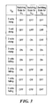
- Fig. 3 represents a chart showing the switching state of first, second and third MOSFETs Q 1 , Q 2 and Q 3 at selected points for input voltage signal V in . Referring to Figs. 1-3, with input voltage V in representing a trapezoidal wave and with the time at zero, input voltage V in is at zero. With input voltage V in at zero, first MOSFET Q 1 , second MOSFET Q 2 and third MOSFET Q 3 are all off. With third MOSFET Q 3 off, no current passes through load resistor R L . As a result, output voltage V out at output terminal 17 will be approximately V cc , discarding any leakage.
- second MOSFET Q 2 will turn on because, with virtually no current in first resistor R 1 , the voltage at gate electrode 29 of second MOSFET Q 2 is approximately the value of input voltage V in .
- second MOSFET Q 2 will have the value of MOSFET threshold voltage V FETTH at gate electrode 29 and, as a consequence, second MOSFET Q 2 will turn on, with first MOSFET Q 1 and third MOSFET Q 3 remaining off.
- current will flow through second resistor R 2 and third resistor R 3 .
- Second resistor R 2 and third resistor R 3 together act as voltage dividers. As a result, voltage at the junction of second resistor R 2 and third resistor R 3 will then pass into gate electrodes 23 and 35 of first and third MOSFETs Q 1 and Q 3 , respectively, with gate electrode 35 of third MOSFET Q 3 receiving approximately 1 ⁇ 2 of input voltage V in and gate electrode 23 of first MOSFET Q 1 also receiving approximately 1 ⁇ 2 of input voltage V in .
- first and third MOSFETs Q 1 and Q 3 will turn on once input voltage V in equals approximately 2.1 x MOSFET threshold voltage V FETTH (approximately 2.5 volts), this value of V in being identified as the rising threshold voltage V TH+ for switch 11 in Fig. 2.
- first MOSFET Q 1 turns on, first MOSFET Q 1 pulls down the voltage at gate electrode 29 of second MOSFET Q 2 until second MOSFET Q 2 turns off. With second MOSFET Q 2 off, no current flows through third resistor R 3 .
- third MOSFET Q 3 will turn off once input voltage V in equals approximately 1.1 x MOSFET threshold voltage V FETTH (approximately 1.3 volts), this value of V in being identified as the falling threshold voltage V TH- for switch 11 in Fig. 2.
- gate 35 at third MOSFET Q 3 has a voltage of approximately MOSFET threshold voltage V FETTH .
- first MOSFET Q 1 will turn off.
- second MOSFET Q 2 will turn back on.
- the voltage at gate electrode 35 of third MOSFET Q 3 will lower, thereby making first and third MOSFETs Q 1 and Q 3 turn off.
- output voltage V out at output terminal 17 will abruptly return to approximately V cc , as shown in Fig. 2, discarding any leakage.
- rising threshold voltage V TH+ (approximately 2.5 volts) is significantly higher than the falling threshold voltage V TH- (approximately 1.3 volts), as shown in Fig. 2.
- V TH- (approximately 1.3 volts)
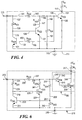
- FIG.4 there is shown a second embodiment of a three-terminal inverting hysteretic transistor switch constructed according to the teachings of the present invention, the switch being identified as reference numeral 111.
- Switch 111 is similar to switch 11 in that switch 111 is also inverting, experiences input signal actuated hysteresis and comprises only three terminals.
- switch 111 comprises a first bipolar junction transistor (BJT) Q 101 , a second bipolar junction transistor (BJT) Q 102 and a third bipolar junction transistor (BJT) Q 103 in place of first MOSFET Q 1 , second MOSFET Q 2 and third MOSFET Q 3 , respectively, of switch 11.
- switch 11 and switch 111 function in a similar manner.
- switch 11 is shown comprising three MOSFETs and switch 111 is shown comprising three bipolar junction transistors
- additional switch embodiments which comprise combinations of MOSFETs and bipolar junction transistors could readily be manufactured.
- Switch 111 comprises an input terminal 113, a ground terminal 115 and an output terminal 117.
- input terminal 113, ground terminal 115 and output terminal 117 are the only terminals for switch 111, which is an object of the present invention.
- First bipolar junction transistor (BJT) Q 101 , second bipolar junction transistor (BJT) Q 102 and third bipolar junction transistor (BJT) Q 103 are identical. Specifically, first bipolar junction transistor (BJT) Q 101 , second bipolar junction transistor (BJT) Q 102 and third bipolar junction transistor (BJT) Q 103 are all preferably NPN 2N2222-type bipolar junction transistors, each preferably having a BJT threshold voltage V BJTTH of approximately 0.7 volts. However, it is to be understood that first BJT Q 101 , second BJT Q 102 and third BJT Q 103 are not limited to having a threshold voltage of approximately 0.7 volts.
- first BJT Q 101 , second BJT Q 102 and third BJT Q 103 are not limited to having equal threshold voltages. Rather, it is to be understood that first BJT Q 101 , second BJT Q 102 and third BJT Q 103 could each have different threshold voltage values from one another without departing from the spirit of the present invention.
- First BJT Q 101 includes a collector electrode 119, an emitter electrode 121 connected to ground and a base electrode 123.
- Second BJT Q 102 includes a collector electrode 125, an emitter electrode 127 connected to ground and a base electrode 129 connected collector electrode 119 of first BJT Q 101 .
- Third BJT Q 103 includes a collector electrode 131 connected to output terminal 117, an emitter electrode 133 connected to ground terminal 115 and a base electrode 135.
- Switch 111 further comprises a first resistor R 101 , a second resistor R 102 and a third resistor R 103 .
- First resistor R 101 preferably has a value of approximately 1.0 Mohms and includes a first terminal 137 connected to input terminal 113 and a second terminal 139 connected to collector electrode 119 of first BJT Q 101 .
- Second resistor R 102 preferably has a value of approximately 22 Kohms and includes a first terminal 141 connected to input terminal 113 and a second terminal 143 connected to base electrode 135 of third BJT Q 103 .
- Third resistor R 103 preferably has a value of approximately 120 Kohms and includes a first terminal 145 connected to base electrode 135 of third BJT Q 103 and a second terminal 147 connected to collector electrode 125 of second BJT Q 102 .
- Switch 111 additionally comprises a fourth resistor R 104 .
- Fourth resistor R 104 preferably has a value of approximately 120 Kohms and includes a first terminal 149 connected to base electrode 135 of third BJT Q 103 and a second terminal 151 connected to ground. It should be noted that fourth resistor R 104 is required because first BJT Q 101 , second BJT Q 102 and third BJT Q 103 are identical. However, if first BJT Q 101 , second BJT Q 102 and third BJT Q 103 had unequal turn-on threshold voltage values which would result in second BJT Q 102 turning on before first BJT Q 101 and third BJT Q 103 during use, fourth resistor R 104 could be eliminated from switch 111.
- Output terminal 117 can be connected through a load resistor R L to a supply voltage V CC , load resistor R L preferably having a value of 1.0Kohms.
- load resistor R L and supply voltage V CC are external to switch 111 and consequently are not to be considered part of the present invention.
- Switch 111 further comprises a fifth resistor R 105 .
- Fifth resistor R 105 preferably has a value of approximately 1.0 Mohms and includes a first terminal 153 connected to base electrode 135 of third BJT Q 103 and a second terminal 155 connected to base electrode 123 of first BJT Q 101 .
- fifth resistor R 105 could alternatively have a value of zero ohms. If fifth resistor R 105 has a value of zero ohms, first terminal 153 and second terminal 155 are connected together.
- an additional device such as a diode, PNP bipolar transistor, P-channel FET, or programmable unijunction transistor (PUT), could optionally be connected to input terminal 113 and base electrode 135 in parallel with second resistor R 102 . As can be appreciated, the device would serve to assist in removing charge from base electrode 135 of third BJT Q 103 .
- switch 111 functions in a similar manner to switch 11.
- switch 111 similarly has a rising threshold voltage which is significantly higher than its falling threshold voltage, as shown in Fig. 5.
- a noisy input signal will not cause switch 111 to experience unwanted state changes, which is desirable.
- Switch 211 is similar to switch 111 in that switch 211 is also inverting, experiences input signal actuated hysteresis and comprises only three terminals.
- Switch 211 is similar to switch 111 in that switch 211 comprises an input terminal 213, a ground terminal 215 and an output terminal 217.
- input terminal 213, ground terminal 215 and output terminal 217 are the only terminals for switch 211, which is an object of the present invention.
- Switch 211 is similar to switch 111 in that switch 211 comprises a first bipolar junction transistor (BJT) Q 201 and a second bipolar junction transistor (BJT) Q 202 which are identical in construction with first BJT Q 101 and second BJT Q 102 of switch 111.
- first BJT Q 201 and second BJT Q 202 are both NPN 2N2222-type bipolar junction transistors, each preferably having a BJT threshold voltage V BJTTH of approximately 0.7 volts.
- first BJT Q 201 and second BJT Q 202 are not limited to having a threshold voltage of approximately 0.7 volts.
- first BJT Q 201 and second BJT Q 202 are not limited to having equal threshold voltages. Rather, it is to be understood that first BJT Q 201 and second BJT Q 202 could each have different threshold voltage values from one another.
- First BJT Q 201 includes a collector electrode 219, an emitter electrode 221 connected to ground and a base electrode 223.
- Second BJT Q 202 includes a collector electrode 225, an emitter electrode 227 connected to ground and a base electrode 229 connected to collector electrode 219 of first BJT Q 201 .
- Switch 211 also comprises a first resistor R 201 , a second resistor R 202 and a third resistor R 203 .
- First resistor R 201 preferably has a value of approximately 1.0 Mohms and includes a first terminal 231 connected to input terminal 213 and a second terminal 233 connected to collector electrode 219 of first BJT Q 201 .
- Second resistor R 202 preferably has a value of approximately 120 Kohms and includes a first terminal 235 connected to input terminal 213 and a second terminal 237.
- Third resistor R 203 preferably has a value of approximately 1.0 Mohms and includes a first terminal 239 connected to second terminal 237 of second resistor R 202 and a second terminal 241 connected to collector terminal 225 of second BJT Q 202 .
- switch 211 comprises a Darlington-connected compound bipolar junction transistor Q 203 in place of third BJT Q 103 of switch 111.
- Darlington-connected compound BJT Q 203 is desirable in that it has twice the turn-on threshold voltage of either first BJT Q 201 or second BJT Q 202 .
- no resistor is required in switch 211 to perform the function performed by fourth resistor R 104 in switch 111.
- Darlington-connected compound BJT Q 203 is also desirable because it can switch relatively high current and voltage with small die area.
- Darlington-connected compound BJT Q 203 comprises a fourth BJT Q 204 and a fifth BJT Q 205 .
- fourth BJT Q 204 and fifth BJT Q 205 are both NPN TIP121-type bipolar junction transistors, each preferably having a BJT threshold voltage V BJTTH of approximately 1.4 volts or approximately two times the voltage of the threshold voltage of first BJT Q 201 and second BJT Q 202 .
- Fourth BJT Q 204 includes a collector electrode 243 connected to output terminal 217, an emitter electrode 245 and a base electrode 247 connected to second terminal 237 of second resistor R 202 .
- Fifth BJT Q 205 includes a collector electrode 249 connected to output terminal 217, an emitter electrode 251 connected to ground and a base electrode 253 connected to emitter electrode 245 of fourth BJT Q 204 .
- Switch 111 additionally comprises a fourth resistor R 204 and a fifth resistor R 205 which together act as a resistor divider for increasing the effective turn-on voltage threshold of first BJT Q 201 .
- Fourth resistor R 204 preferably has a value of approximately 1.0 Mohms and includes a first terminal 257 connected to base electrode 247 of fourth BJT Q 204 and a second terminal 259 connected to base electrode 223 of first BJT Q 201 .
- Fifth resistor R 205 preferably has a value of approximately 1.0 Mohms and includes a first terminal 261 connected to second terminal 259 of fourth resistor R 204 and a second terminal 263 connected to ground.
- Output terminal 217 can be connected through a load resistor R L to a supply voltage V CC , load resistor R L preferably having a value of 1.0Kohms.
- load resistor R L and supply voltage V CC are external to switch 211 and consequently are not to be considered part of the present invention.
- an additional device such as a diode, PNP bipolar transistor, P-channel FET, or programmable unijunction transistor (PUT), could optionally be connected to input terminal 213 and base electrode 247 in parallel with second resistor R 202 without departing from the spirit of the present invention. As can be appreciated, the device would serve to assist in removing charge from base electrode 247 of fourth BJT Q 204 .
- switch 211 functions in a similar manner to switch 111.
- switch 211 similarly has a rising threshold voltage which is significantly higher than its falling threshold voltage. As a result, a noisy input signal will not cause switch 211 to experience unwanted state changes, which is desirable.
Landscapes
- Engineering & Computer Science (AREA)
- Power Engineering (AREA)
- Electronic Switches (AREA)
- Manipulation Of Pulses (AREA)
- Logic Circuits (AREA)
Claims (10)
- Invertierender hysteretischer Transistorschalter (11) mit nur drei Anschlüssen, wobei die drei Anschlüsse ein Eingangsanschluß (13), ein Ausgangsanschluß (17) und ein Masseanschluß (15) sind, wobei der invertierende hysteretische Transistorschalter folgendes umfaßt:a. einen ersten Feldeffekttransistor bzw. FET (Q1) mit einem Drainanschluß, einem Sourceanschluß und einem Gateanschluß, wobei der Sourceanschluß des ersten FET mit dem Masseanschluß verbunden ist;b. einen zweiten Feldeffekttransistor bzw. FET (Q2) mit einem Drainanschluß, einem Sourceanschluß und einem Gateanschluß, wobei der Sourceanschluß des zweiten FET mit dem Masseanschluß und der Gateanschluß des zweiten FET mit dem Drainanschluß des ersten FET verbunden ist;c. einen dritten Feldeffekttransistor bzw. FET (Q3) mit einem Drainanschluß, einem Sourceanschluß und einem Gateanschluß, wobei der Sourceanschluß des dritten FET mit dem Masseanschluß verbunden ist, der Drainanschluß des dritten FET mit dem Ausgangsanschluß verbunden ist und der Gateanschluß (35) des dritten FET mit dem Gateanschluß (22) des ersten FET verbunden ist;d. einen ersten Widerstand (R1) mit einem ersten Anschluß und einem zweiten Anschluß, wobei der erste Anschluß des ersten Widerstands mit dem Eingangsanschluß und der zweite Anschluß des ersten Widerstands mit dem Drainanschluß (19) des ersten FET verbunden ist;e. einen zweiten Widerstand (R2) mit einem ersten Anschluß und einem zweiten Anschluß, wobei der erste Anschluß des zweiten Widerstands mit dem Eingangsanschluß und der zweite Anschluß des zweiten Widerstands mit dem Gateanschluß (23) des ersten FET verbunden ist; undf. einen dritten Widerstand (R3) mit einem ersten Anschluß und einem zweiten Anschluß, wobei der erste Anschluß des dritten Widerstands mit dem Gateanschluß (23) des ersten FET verbunden ist und der zweite Anschluß des dritten Widerstands mit dem Drainanschluß (25) des zweiten FET verbunden ist.
- Invertierender hysteretischer Transistorschalter nach Anspruch 1, wobei jeder des ersten, des zweiten und des dritten Feldeffekttransistors N-Kanal-Metalloxid-Halbleiterfeldeffekttransistoren des Anreichungsmodus (MOSFET) sind.
- Invertierender hysteretischer Transistorschalter nach Anspruch 2, wobei der erste, der zweite und der dritte Feldeffekttransistor (FET) gleiche Schwellenspannungen aufweisen.
- Invertierender hysteretischer Transistorschalter nach Anspruch 3, wobei der erste, der zweite und der dritte Widerstand ungefähr 120 kOhm betragen.
- Invertierender hysteretischer Transistorschalter nach Anspruch 4, ferner mit einem vierten Widerstand (R4) mit einem ersten Anschluß und einem zweiten Anschluß, wobei der erste Anschluß des vierten Widerstands mit dem Gateanschluß (35) des dritten FET und der zweite Anschluß des vierten Widerstands mit Masse verbunden ist.
- Invertierender hysteretischer Transistorschalter (111, 211) mit nur drei Anschlüssen, wobei die drei Anschlüsse ein Eingangsanschluß (113, 213), ein Ausgangsanschluß (117, 217) und ein Masseanschluß (115, 215) sind, wobei der invertierende hysteretische Transistorschalter folgendes umfaßt:a. einen ersten Transistor (Q101, Q201) mit einer Kollektorelektrode (119, 219), einer Basiselektrode (123, 223) und einer Emitterelektrode (121, 221), die mit dem Masseanschluß verbunden ist;b. einen zweiten Transistor (Q102, Q202) mit einer Kollektorelektrode (125, 225), einer mit der Kollektorelektrode des ersten Transistors verbundenen Basiselektrode (129, 229) und einer mit dem Masseanschluß verbundenen Emitterelektrode (127, 227);c. einen dritten Transistor (Q103, Q203) mit einer mit dem Ausgangsanschluß verbundenen Kollektorelektrode (131, 243, 249), einer mit der Basiselektrode des ersten Transistors verbundenen Basiselektrode (135, 247) und einer mit dem Masseanschluß verbundenen Emitterelektrode (133, 251);d. einen ersten Widerstand (R101, R201), mit einem mit dem Eingangsanschluß verbundenen ersten Anschluß (137, 231) und einem mit der Kollektorelektrode des ersten Transistors verbundenen zweiten Anschluß;e. einen zweiten Widerstand (R102, R202) mit einem mit dem Eingangsanschluß verbundenen ersten Anschluß (141, 235) und einem mit der Basiselektrode des dritten Transistors verbundenen zweiten Anschluß (143, 237); undf. einen dritten Widerstand (R103, R203) mit einem mit der Basiselektrode des dritten Transistors verbundenen ersten Anschluß (145, 239) und einem mit der Kollektorelektrode des zweiten Transistors verbundenen zweiten Anschluß (125, 241).
- Invertierender hysteretischer Transistorschalter nach Anspruch 6, wobei der dritte Transistor ein Verbund-Bipolar-Sperrschichttransistor in Darlington-Schaltung ist.
- Invertierender hysteretischer Transistorschalter nach Anspruch 7, wobei die Basiselektrode (135,247) des dritten Transistors durch einen vierten Widerstand (R105, R204) mit einem mit der Basiselektrode des dritten Transistors verbundenen ersten Anschluß (153, 257) und einem mit der Basiselektrode des ersten Transistors verbundenen zweiten Anschluß (155, 261) mit der Basiselektrode (123, 223) des ersten Transistors verbunden ist.
- Invertierender hysteretischer Transistorschalter nach Anspruch 8, ferner mit einem fünften Widerstand (R205) mit einem mit dem zweiten Anschluß des vierten Widerstands verbundenen ersten Anschluß (261) und einem mit dem Masseanschluß verbundenen zweiten Anschluß (263).
- Invertierender hysteretischer Transistorschalter nach Anspruch 6, wobei jeder des ersten, des zweiten und des dritten Transistors ein NPN-Bipolar-Sperrschichttransistor (BJT) ist.
Applications Claiming Priority (1)
| Application Number | Priority Date | Filing Date | Title |
|---|---|---|---|
| PCT/US2000/020203 WO2002009282A1 (en) | 2000-07-25 | 2000-07-25 | Three-terminal inverting hysteretic transistor switch |
Publications (3)
| Publication Number | Publication Date |
|---|---|
| EP1329023A1 EP1329023A1 (de) | 2003-07-23 |
| EP1329023A4 EP1329023A4 (de) | 2005-12-07 |
| EP1329023B1 true EP1329023B1 (de) | 2007-05-09 |
Family
ID=21741614
Family Applications (1)
| Application Number | Title | Priority Date | Filing Date |
|---|---|---|---|
| EP00957252A Expired - Lifetime EP1329023B1 (de) | 2000-07-25 | 2000-07-25 | Invertierender hysteretischer transistorschalter mit drei anschlüssen hintergrund der erfindung |
Country Status (5)
| Country | Link |
|---|---|
| EP (1) | EP1329023B1 (de) |
| JP (1) | JP2004511121A (de) |
| CA (1) | CA2417378C (de) |
| DE (1) | DE60034822T2 (de) |
| WO (1) | WO2002009282A1 (de) |
Families Citing this family (1)
| Publication number | Priority date | Publication date | Assignee | Title |
|---|---|---|---|---|
| JP5864006B1 (ja) * | 2015-04-06 | 2016-02-17 | 国立大学法人東京工業大学 | 直流電力系の安全装置 |
Family Cites Families (3)
| Publication number | Priority date | Publication date | Assignee | Title |
|---|---|---|---|---|
| JPS62114324A (ja) * | 1985-11-13 | 1987-05-26 | Omron Tateisi Electronics Co | 出力制御回路 |
| JPS62114323A (ja) * | 1985-11-13 | 1987-05-26 | Omron Tateisi Electronics Co | 出力制御回路 |
| US5952870A (en) * | 1997-12-29 | 1999-09-14 | Motorola, Inc. | Circuit with hysteresis and method using same |
-
2000
- 2000-07-25 DE DE60034822T patent/DE60034822T2/de not_active Expired - Lifetime
- 2000-07-25 CA CA002417378A patent/CA2417378C/en not_active Expired - Lifetime
- 2000-07-25 JP JP2002514885A patent/JP2004511121A/ja active Pending
- 2000-07-25 EP EP00957252A patent/EP1329023B1/de not_active Expired - Lifetime
- 2000-07-25 WO PCT/US2000/020203 patent/WO2002009282A1/en not_active Ceased
Also Published As
| Publication number | Publication date |
|---|---|
| JP2004511121A (ja) | 2004-04-08 |
| CA2417378A1 (en) | 2002-01-31 |
| CA2417378C (en) | 2005-04-05 |
| EP1329023A4 (de) | 2005-12-07 |
| DE60034822D1 (de) | 2007-06-21 |
| DE60034822T2 (de) | 2008-01-17 |
| EP1329023A1 (de) | 2003-07-23 |
| WO2002009282A1 (en) | 2002-01-31 |
Similar Documents
| Publication | Publication Date | Title |
|---|---|---|
| JP2821714B2 (ja) | 交差導通電流を減少させる電力用mosfet駆動回路 | |
| US8466735B2 (en) | High temperature gate drivers for wide bandgap semiconductor power JFETs and integrated circuits including the same | |
| WO1995031852A1 (en) | Load driving device | |
| KR900008801B1 (ko) | 논리회로 | |
| US6259292B1 (en) | Three-terminal inverting hysteretic transistor switch | |
| JP2002208849A (ja) | 誘導性負荷駆動回路 | |
| US7705638B2 (en) | Switching control circuit with reduced dead time | |
| US6326819B1 (en) | Current buffer for gate drive | |
| EP1329023B1 (de) | Invertierender hysteretischer transistorschalter mit drei anschlüssen hintergrund der erfindung | |
| JP2002084174A (ja) | 負荷駆動回路 | |
| JP3258050B2 (ja) | 誘導性負荷用mosfetを備えた回路装置 | |
| EP0432472B1 (de) | Integrierte CMOS-Ausgangsschaltung mit bipolaren Transistoren in der Ausgangsstufe | |
| JPH0446486B2 (de) | ||
| CN113491049A (zh) | 用于保护开关的关断电路 | |
| JP3806108B2 (ja) | 半導体リレー装置 | |
| JPS6249966B2 (de) | ||
| US3428832A (en) | Electronic switching circuit employing insulated gate field effect transistors | |
| JP3036556B2 (ja) | Nチャンネル形fetの駆動制御回路 | |
| JPH01144815A (ja) | Cmosトランジスタを使用したラッチ形スイッチ | |
| JP3113062B2 (ja) | スイッチ回路 | |
| JPH0330881Y2 (de) | ||
| JPH02240478A (ja) | ラッチ弁の駆動回路 | |
| JPS6139622A (ja) | 電子タイマ | |
| JPS62118787A (ja) | 絶縁ゲ−ト電界効果トランジスタおよびコイルを備えた回路 | |
| JPH04324713A (ja) | 光結合型リレー回路 |
Legal Events
| Date | Code | Title | Description |
|---|---|---|---|
| PUAI | Public reference made under article 153(3) epc to a published international application that has entered the european phase |
Free format text: ORIGINAL CODE: 0009012 |
|
| 17P | Request for examination filed |
Effective date: 20030218 |
|
| AK | Designated contracting states |
Designated state(s): AT BE CH CY DE DK ES FI FR GB GR IE IT LI LU MC NL PT SE |
|
| AX | Request for extension of the european patent |
Extension state: AL LT LV MK RO SI |
|
| RBV | Designated contracting states (corrected) |
Designated state(s): AT BE CH CY DE FR GB IT LI |
|
| A4 | Supplementary search report drawn up and despatched |
Effective date: 20051024 |
|
| GRAP | Despatch of communication of intention to grant a patent |
Free format text: ORIGINAL CODE: EPIDOSNIGR1 |
|
| RBV | Designated contracting states (corrected) |
Designated state(s): DE FR GB IT |
|
| GRAS | Grant fee paid |
Free format text: ORIGINAL CODE: EPIDOSNIGR3 |
|
| GRAA | (expected) grant |
Free format text: ORIGINAL CODE: 0009210 |
|
| AK | Designated contracting states |
Kind code of ref document: B1 Designated state(s): DE FR GB IT |
|
| REG | Reference to a national code |
Ref country code: GB Ref legal event code: FG4D |
|
| REF | Corresponds to: |
Ref document number: 60034822 Country of ref document: DE Date of ref document: 20070621 Kind code of ref document: P |
|
| ET | Fr: translation filed | ||
| PLBE | No opposition filed within time limit |
Free format text: ORIGINAL CODE: 0009261 |
|
| STAA | Information on the status of an ep patent application or granted ep patent |
Free format text: STATUS: NO OPPOSITION FILED WITHIN TIME LIMIT |
|
| 26N | No opposition filed |
Effective date: 20080212 |
|
| REG | Reference to a national code |
Ref country code: FR Ref legal event code: PLFP Year of fee payment: 16 |
|
| REG | Reference to a national code |
Ref country code: FR Ref legal event code: PLFP Year of fee payment: 17 |
|
| PGFP | Annual fee paid to national office [announced via postgrant information from national office to epo] |
Ref country code: FR Payment date: 20160613 Year of fee payment: 17 |
|
| PGFP | Annual fee paid to national office [announced via postgrant information from national office to epo] |
Ref country code: DE Payment date: 20160720 Year of fee payment: 17 Ref country code: IT Payment date: 20160720 Year of fee payment: 17 Ref country code: GB Payment date: 20160720 Year of fee payment: 17 |
|
| REG | Reference to a national code |
Ref country code: DE Ref legal event code: R119 Ref document number: 60034822 Country of ref document: DE |
|
| GBPC | Gb: european patent ceased through non-payment of renewal fee |
Effective date: 20170725 |
|
| REG | Reference to a national code |
Ref country code: FR Ref legal event code: ST Effective date: 20180330 |
|
| PG25 | Lapsed in a contracting state [announced via postgrant information from national office to epo] |
Ref country code: GB Free format text: LAPSE BECAUSE OF NON-PAYMENT OF DUE FEES Effective date: 20170725 Ref country code: DE Free format text: LAPSE BECAUSE OF NON-PAYMENT OF DUE FEES Effective date: 20180201 |
|
| PG25 | Lapsed in a contracting state [announced via postgrant information from national office to epo] |
Ref country code: FR Free format text: LAPSE BECAUSE OF NON-PAYMENT OF DUE FEES Effective date: 20170731 |
|
| PG25 | Lapsed in a contracting state [announced via postgrant information from national office to epo] |
Ref country code: IT Free format text: LAPSE BECAUSE OF NON-PAYMENT OF DUE FEES Effective date: 20170725 |