EP1329538A2 - Procédé pour fabriquer des cristaux formés par une injection vers le haut de liquide sous pression - Google Patents
Procédé pour fabriquer des cristaux formés par une injection vers le haut de liquide sous pression Download PDFInfo
- Publication number
- EP1329538A2 EP1329538A2 EP03007764A EP03007764A EP1329538A2 EP 1329538 A2 EP1329538 A2 EP 1329538A2 EP 03007764 A EP03007764 A EP 03007764A EP 03007764 A EP03007764 A EP 03007764A EP 1329538 A2 EP1329538 A2 EP 1329538A2
- Authority
- EP
- European Patent Office
- Prior art keywords
- shaper
- crystal
- melt
- fabricating
- crystals
- Prior art date
- Legal status (The legal status is an assumption and is not a legal conclusion. Google has not performed a legal analysis and makes no representation as to the accuracy of the status listed.)
- Withdrawn
Links
Images




Classifications
-
- C—CHEMISTRY; METALLURGY
- C30—CRYSTAL GROWTH
- C30B—SINGLE-CRYSTAL GROWTH; UNIDIRECTIONAL SOLIDIFICATION OF EUTECTIC MATERIAL OR UNIDIRECTIONAL DEMIXING OF EUTECTOID MATERIAL; REFINING BY ZONE-MELTING OF MATERIAL; PRODUCTION OF A HOMOGENEOUS POLYCRYSTALLINE MATERIAL WITH DEFINED STRUCTURE; SINGLE CRYSTALS OR HOMOGENEOUS POLYCRYSTALLINE MATERIAL WITH DEFINED STRUCTURE; AFTER-TREATMENT OF SINGLE CRYSTALS OR A HOMOGENEOUS POLYCRYSTALLINE MATERIAL WITH DEFINED STRUCTURE; APPARATUS THEREFOR
- C30B29/00—Single crystals or homogeneous polycrystalline material with defined structure characterised by the material or by their shape
- C30B29/02—Elements
- C30B29/06—Silicon
-
- C—CHEMISTRY; METALLURGY
- C30—CRYSTAL GROWTH
- C30B—SINGLE-CRYSTAL GROWTH; UNIDIRECTIONAL SOLIDIFICATION OF EUTECTIC MATERIAL OR UNIDIRECTIONAL DEMIXING OF EUTECTOID MATERIAL; REFINING BY ZONE-MELTING OF MATERIAL; PRODUCTION OF A HOMOGENEOUS POLYCRYSTALLINE MATERIAL WITH DEFINED STRUCTURE; SINGLE CRYSTALS OR HOMOGENEOUS POLYCRYSTALLINE MATERIAL WITH DEFINED STRUCTURE; AFTER-TREATMENT OF SINGLE CRYSTALS OR A HOMOGENEOUS POLYCRYSTALLINE MATERIAL WITH DEFINED STRUCTURE; APPARATUS THEREFOR
- C30B11/00—Single-crystal growth by normal freezing or freezing under temperature gradient, e.g. Bridgman-Stockbarger method
-
- C—CHEMISTRY; METALLURGY
- C30—CRYSTAL GROWTH
- C30B—SINGLE-CRYSTAL GROWTH; UNIDIRECTIONAL SOLIDIFICATION OF EUTECTIC MATERIAL OR UNIDIRECTIONAL DEMIXING OF EUTECTOID MATERIAL; REFINING BY ZONE-MELTING OF MATERIAL; PRODUCTION OF A HOMOGENEOUS POLYCRYSTALLINE MATERIAL WITH DEFINED STRUCTURE; SINGLE CRYSTALS OR HOMOGENEOUS POLYCRYSTALLINE MATERIAL WITH DEFINED STRUCTURE; AFTER-TREATMENT OF SINGLE CRYSTALS OR A HOMOGENEOUS POLYCRYSTALLINE MATERIAL WITH DEFINED STRUCTURE; APPARATUS THEREFOR
- C30B11/00—Single-crystal growth by normal freezing or freezing under temperature gradient, e.g. Bridgman-Stockbarger method
- C30B11/007—Mechanisms for moving either the charge or the heater
-
- C—CHEMISTRY; METALLURGY
- C30—CRYSTAL GROWTH
- C30B—SINGLE-CRYSTAL GROWTH; UNIDIRECTIONAL SOLIDIFICATION OF EUTECTIC MATERIAL OR UNIDIRECTIONAL DEMIXING OF EUTECTOID MATERIAL; REFINING BY ZONE-MELTING OF MATERIAL; PRODUCTION OF A HOMOGENEOUS POLYCRYSTALLINE MATERIAL WITH DEFINED STRUCTURE; SINGLE CRYSTALS OR HOMOGENEOUS POLYCRYSTALLINE MATERIAL WITH DEFINED STRUCTURE; AFTER-TREATMENT OF SINGLE CRYSTALS OR A HOMOGENEOUS POLYCRYSTALLINE MATERIAL WITH DEFINED STRUCTURE; APPARATUS THEREFOR
- C30B29/00—Single crystals or homogeneous polycrystalline material with defined structure characterised by the material or by their shape
- C30B29/02—Elements
- C30B29/08—Germanium
-
- C—CHEMISTRY; METALLURGY
- C30—CRYSTAL GROWTH
- C30B—SINGLE-CRYSTAL GROWTH; UNIDIRECTIONAL SOLIDIFICATION OF EUTECTIC MATERIAL OR UNIDIRECTIONAL DEMIXING OF EUTECTOID MATERIAL; REFINING BY ZONE-MELTING OF MATERIAL; PRODUCTION OF A HOMOGENEOUS POLYCRYSTALLINE MATERIAL WITH DEFINED STRUCTURE; SINGLE CRYSTALS OR HOMOGENEOUS POLYCRYSTALLINE MATERIAL WITH DEFINED STRUCTURE; AFTER-TREATMENT OF SINGLE CRYSTALS OR A HOMOGENEOUS POLYCRYSTALLINE MATERIAL WITH DEFINED STRUCTURE; APPARATUS THEREFOR
- C30B29/00—Single crystals or homogeneous polycrystalline material with defined structure characterised by the material or by their shape
- C30B29/10—Inorganic compounds or compositions
- C30B29/46—Sulfur-, selenium- or tellurium-containing compounds
-
- C—CHEMISTRY; METALLURGY
- C30—CRYSTAL GROWTH
- C30B—SINGLE-CRYSTAL GROWTH; UNIDIRECTIONAL SOLIDIFICATION OF EUTECTIC MATERIAL OR UNIDIRECTIONAL DEMIXING OF EUTECTOID MATERIAL; REFINING BY ZONE-MELTING OF MATERIAL; PRODUCTION OF A HOMOGENEOUS POLYCRYSTALLINE MATERIAL WITH DEFINED STRUCTURE; SINGLE CRYSTALS OR HOMOGENEOUS POLYCRYSTALLINE MATERIAL WITH DEFINED STRUCTURE; AFTER-TREATMENT OF SINGLE CRYSTALS OR A HOMOGENEOUS POLYCRYSTALLINE MATERIAL WITH DEFINED STRUCTURE; APPARATUS THEREFOR
- C30B29/00—Single crystals or homogeneous polycrystalline material with defined structure characterised by the material or by their shape
- C30B29/60—Single crystals or homogeneous polycrystalline material with defined structure characterised by the material or by their shape characterised by shape
-
- H—ELECTRICITY
- H10—SEMICONDUCTOR DEVICES; ELECTRIC SOLID-STATE DEVICES NOT OTHERWISE PROVIDED FOR
- H10N—ELECTRIC SOLID-STATE DEVICES NOT OTHERWISE PROVIDED FOR
- H10N10/00—Thermoelectric devices comprising a junction of dissimilar materials, i.e. devices exhibiting Seebeck or Peltier effects
- H10N10/01—Manufacture or treatment
-
- H—ELECTRICITY
- H10—SEMICONDUCTOR DEVICES; ELECTRIC SOLID-STATE DEVICES NOT OTHERWISE PROVIDED FOR
- H10N—ELECTRIC SOLID-STATE DEVICES NOT OTHERWISE PROVIDED FOR
- H10N10/00—Thermoelectric devices comprising a junction of dissimilar materials, i.e. devices exhibiting Seebeck or Peltier effects
- H10N10/10—Thermoelectric devices comprising a junction of dissimilar materials, i.e. devices exhibiting Seebeck or Peltier effects operating with only the Peltier or Seebeck effects
- H10N10/17—Thermoelectric devices comprising a junction of dissimilar materials, i.e. devices exhibiting Seebeck or Peltier effects operating with only the Peltier or Seebeck effects characterised by the structure or configuration of the cell or thermocouple forming the device
-
- F—MECHANICAL ENGINEERING; LIGHTING; HEATING; WEAPONS; BLASTING
- F25—REFRIGERATION OR COOLING; COMBINED HEATING AND REFRIGERATION SYSTEMS; HEAT PUMP SYSTEMS; MANUFACTURE OR STORAGE OF ICE; LIQUEFACTION SOLIDIFICATION OF GASES
- F25B—REFRIGERATION MACHINES, PLANTS OR SYSTEMS; COMBINED HEATING AND REFRIGERATION SYSTEMS; HEAT PUMP SYSTEMS
- F25B21/00—Machines, plants or systems, using electric or magnetic effects
- F25B21/02—Machines, plants or systems, using electric or magnetic effects using Peltier effect; using Nernst-Ettinghausen effect
-
- F—MECHANICAL ENGINEERING; LIGHTING; HEATING; WEAPONS; BLASTING
- F25—REFRIGERATION OR COOLING; COMBINED HEATING AND REFRIGERATION SYSTEMS; HEAT PUMP SYSTEMS; MANUFACTURE OR STORAGE OF ICE; LIQUEFACTION SOLIDIFICATION OF GASES
- F25D—REFRIGERATORS; COLD ROOMS; ICE-BOXES; COOLING OR FREEZING APPARATUS NOT OTHERWISE PROVIDED FOR
- F25D11/00—Self-contained movable devices, e.g. domestic refrigerators
-
- Y—GENERAL TAGGING OF NEW TECHNOLOGICAL DEVELOPMENTS; GENERAL TAGGING OF CROSS-SECTIONAL TECHNOLOGIES SPANNING OVER SEVERAL SECTIONS OF THE IPC; TECHNICAL SUBJECTS COVERED BY FORMER USPC CROSS-REFERENCE ART COLLECTIONS [XRACs] AND DIGESTS
- Y10—TECHNICAL SUBJECTS COVERED BY FORMER USPC
- Y10T—TECHNICAL SUBJECTS COVERED BY FORMER US CLASSIFICATION
- Y10T117/00—Single-crystal, oriented-crystal, and epitaxy growth processes; non-coating apparatus therefor
- Y10T117/10—Apparatus
- Y10T117/1024—Apparatus for crystallization from liquid or supercritical state
- Y10T117/1032—Seed pulling
- Y10T117/1036—Seed pulling including solid member shaping means other than seed or product [e.g., EDFG die]
Definitions
- the present invention relates to a method of fabricating a semiconductor monocrystal or multicrystal of a material such as silicon, germanium, or bismuth telluride, and, in particular, to a method of fabricating a semiconductor crystal that is formed to have a predetermined shape.
- a method of fabricating a large number of cube-shaped monocrystal pieces with sides on the order of 1 to 3 mm is known in the prior art as a method of fabricating pieces of a semiconductor crystal, such as a monocrystal or multicrystal semiconductor of a bismuth/tellurium compound; which involves slicing an ingot of monocrystal or multicrystal grown in an a-axial direction by a downward-drawing method to form circular plates, then dicing these circular plates.
- EFG Edge-defined Film-fed Growth
- crosscut methods are also known in the prior art as methods of fabricating sheets of semiconductor crystal such as silicon ribbon crystals.
- the silicon melt solidifies at a speed of ten to several hundred mm/minute with the above EFG and crosscut methods, so the grain size of the completed crystals is small and thermal stresses still remain therein, and thus quality is poor.
- the present invention was devised in the light of the above problems and has as an objective thereof the provision of an inexpensive method of fabricating shaped crystals of a needle shape (diameter: approximately 0.5 mm to 3 mm) or sheet shape (thickness: approximately 0.5 mm) from a high-quality bismuth/tellurium compound or other semiconductor.
- This invention concerns a method of fabricating a shaped crystal by overhead-pressure liquid injection, comprising the steps of heating a raw crystal material within a shaping vessel set in a predetermined atmosphere, to form a melt; pressuring the melt from overhead, to inject the same into a shaper disposed within the shaping vessel; and a step of cooling the melt injected into the shaper, for form a crystal.
- the method according to the invention is characterized by configuring the shaper of a linked series of a plurality of plate members formed to have steps of predetermined dimensions along left and right edges thereof.
- the melt could be injected inward from above or below the shaper.
- the pressuring during this time could be performed by a mechanical force or by the use of a gas pressure that is set by means for setting the atmosphere of the shaping vessel.
- a plurality of sheet crystals can be fabricated simultaneously.
- the present invention can thus be used to fabricate a number of shaped crystals simultaneously, fabrication costs are reduced.
- the speed of growth of the crystals can also be slowed so that high-quality crystals are obtained.
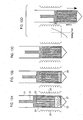
- FIG. 1 A first example of the crystal melt injection method in accordance with this invention is shown in Fig. 1.
- This figure is a section taken in the vertical direction.
- a shaper 2 is disposed within a shaping vessel 1.
- a crystal melt 5, which is present on an upper surface of the shaper 2 is pressed from above by a pressuring member 4.
- a mechanical force F1 is applied to the pressuring member 4 from above.
- the crystal melt 5 is pressed by a lower edge of the pressuring member 4, it has nowhere to escape but a gap 3 formed in the shaper 2, so it is injected into the gap 3 as shown by the arrow in Fig. 1.
- FIG. 2 A second example of the crystal melt injection method in accordance with this invention is shown in Fig. 2.
- the shaper 2 which is present on the upper surface of the crystal melt 5, is pressed from above by the pressuring member 4.
- the mechanical force F1 is applied to the pressuring member 4 from above.
- the shaper 2 is pressed by a lower edge of the pressuring member 4, it moves downward into the vessel 1.
- the crystal melt 5 has nowhere to escape but the gap 3 formed by the shaper 2, so it is injected into the gap 3 as shown by the arrow in Fig. 2.
- FIG. 3 A third example of the crystal melt injection method in accordance with this invention is shown in Fig. 3.
- the crystal melt 5 which is present on an upper surface of the shaper 2 is pressed from above by a pressuring member 6.
- a gas pressure F2 is applied to the pressuring member 6.
- the crystal melt 5 is pressed by a lower edge of the pressuring member 6, it has nowhere to escape but the gap 3 formed by the shaper 2, so it is injected into the gap 3 as shown by the arrow in Fig. 3.
- the raw material for the crystal is first placed between the shaper 2 and the pressuring member 6, and it is also placed on top of the pressuring member 6.
- the interior of a chamber 8 is evacuated by the operation of a vacuum pump 11.
- the raw material of the crystal is then melted by a heating means (not shown in the figure) provided around the shaping vessel 1.
- a valve 10 is opened to introduce argon gas, which is within a gas cylinder 9, into the chamber 8. Since the lower surface of the pressuring member 6 is in a vacuum, the gas pressure of the argon gas moves it to below the pressuring member 6.
- a part7 of the molten raw crystal material acts to block a gap between the pressuring member 6 and an inner wall of the shaping vessel 1, so that there are no problems, even with components that have a bad machining accuracy and a lower level of airtightness.
- the present embodiment is designed to inject a melt of a thermoelectric semiconductor crystal such as bismuth telluride from below into the interior of a shaper, to fabricate a large number of needle monocrystals simultaneously.
- a thermoelectric semiconductor crystal such as bismuth telluride
- a shaping vessel 22 is provided for accommodating the raw material for the crystal in the interior of a quartz tube 21.
- a shaper 23 for molding the molten raw crystal material into needle shapes is provided in the interior of the shaping vessel 22. The shaper 23 moves downward into the interior of the shaping vessel 22, pressed from above by a pressuring member 25. During this time, the melt in the base portion of the shaping vessel 22 is injected into elongated holes 24 formed in the shaper 23. In other words, this is basically equivalent to the situation shown in Fig. 2.
- Fig. 5 is a perspective view
- Fig. 6 is a vertical cross-sectional view
- Fig. 7 is a plan view
- Fig. 8 shows the dimensions of a conical hole.
- the shaping vessel 22 is made of carbon or a ceramic such as boron nitride and is formed to have a box shape, as shown in Fig. 5 or a circular cylindrical shape.
- a large number (25, in these figures) of a diameter of 5 mm and a depth of 10 mm are provided in a surface of the base of the interior of the shaping vessel 22, as shown in Figs. 6 to 8.
- curved grooves could be cut into both sides of each plate member, apart from the two edges thereof.
- the shape of the grooves could also be triangular or square.
- Figs. 11 and 12 show a configuration in which angular grooves 232 of a triangular section-shaped are cut. In essentials, the shape and dimensions of the grooves can be determined by the shape and dimensions of the needle crystals to be fabricated.
- each plate member 23 in this case, it should be obvious that five grooves could be cut therein as necessary, to correspond to Figs. 6 and 7. It is similarly obvious that five pairs of plate members (i.e. ten plates) could be inserted into the shaping vessel 22.
- the crystal axis that brings out the characteristics of a bismuth/tellurium compound thermoelectric material the best is that in the a-axial direction. It is therefore preferable to grow crystal in such a manner that the a-axis is orientated in the longitudinal direction of the needle crystals. That is why a large number of the conical holes 221 is provided in the lower surface within the shaping vessel 22 of this embodiment, as previously described. It has been verified that, if the thus-configured shaping vessel is used, the action of the conical holes 221 ensures that virtually all of the crystal forms in an orientation close to the a-axis in the direction of the grooves 231 or 232.
- a method of promoting monocrystallization by sharpening a tip portion for crystallization into a conical shape has long been known among the methods of growing crystals by using a vessel, but there are no known examples in which a large quantity of needle monocrystals are crystallized from a large number of seed crystals, as in this embodiment.
- a graphite object ET-10P/ made by Ibiden Co., Ltd. is used as the material of the shaper 23. Since the surfaces of the curved grooves 231,or angular grooves 232 of the shaper 23 are subjected to a surface treatment by coating with a solid lubricating agent, it has been confirmed that there is absolutely no adhesion between the groove portions and the needle crystals and the needle crystals can be removed in a simple manner from the shaper 23.
- the solid lubricating agent used in this case is a boron nitride paint (trade name: Whitey Paint) made by Audek.
- a raw material 27 for fabricating the thermoelectric compound semiconductor monocrystal is placed in the base portion of the shaping vessel 22, a vacuum pump (not shown in the figure) and the heater 26 are operated to remove any impurities from the surfaces of the raw material and any water vapor or oxygen from within the shaping vessel 22, then the raw material 27 is melted while an inert atmosphere that will prevent chemical bonding between the crystal and the shaper 23 is created within the shaping vessel 22.
- an external force F such as gas pressure
- the pressuring member 25 moves the resultant melt 28 in the direction of the shaper 23, as shown in Fig. 13b.
- the melt 28 is injected into the elongated holes 24 formed by the grooves of the shaper 23.
- the shaper 23 is moved as far as the base of the shaping vessel 22, as shown in Fig. 13c, and, once the melt 28 has completely filled the elongated holes 24 of the shaper 23, the quartz tube 21 is gradually moved downward, as shown in Fig. 13d, to cause the melt 28 filling the elongated holes 24 of the shaper 23 to solidify from below.
- the temperature gradient in the vertical direction within the quartz tube 21 (which is on the order of 20 to 40oC/cm for a bismuth/tellurium compound, for example) controls the crystal axis direction to grow in the a-axis direction, due to the provision of conical holes in the lower surface. Note that, instead of lowering the quartz tube 21 in this case, the temperature of the heater 26 could equally well be controlled to cool and solidify the crystals.
- the shaper 23 is removed from the shaping vessel 22 and a large number of needle monocrystals are removed from the elongated holes 24.
- needle multicrystals could also be fabricated by cooling the melt 28 quickly.
- the crystal melt of germanium is injected into the shaper from above, to fabrication a large number of sheet crystals simultaneously.
- a gas cylinder 32 filled with argon gas is connected to a quartz tube 31, as shown in Fig. 14, and this argon gas can be introduced into the quartz tube 31 by opening a valve 33.
- a vacuum pump 34 is also connected/to the quartz tube 31 and the interior of the quartz tube 31 can be evacuated by the operation thereof.
- a heater 35 is provided around the quartz tube 31 (in this figure, it is only shown below it), and the interior of the quartz tube 31 can be held at a predetermined temperature thereby.
- a stand 36 is disposed on a base portion within the quartz tube 31 and a shaping vessel 37 containing a raw crystal material is disposed on this stand 36.
- a shaper 38 for shaping the molten raw crystal material into sheets is provided within the shaping vessel 37.
- the interior of the shaping vessel 37 is shown in detail in Fig. 15, in a state in which a raw germanium crystal material is molten.
- the shaper 38 is placed in a base portion of the interior of the shaping vessel 37.
- a melt 41 of the germanium crystal is above the shaper 38.
- a pressuring plate 40 is disposed above the melt 41 of the germanium crystal, a material 47 such as lithium fluoride or potassium chloride is disposed thereabove, and a pressuring member 39 is disposed above that.
- this configuration is basically equivalent to that of Fig. 1, except that the melt is disposed about the shaper as shown in Fig. 2.
- the shaping vessel 37 is formed in a box shape of carbon or a ceramic such as boron nitride, in the same manner as in the first embodiment.
- the shaper 38 is of graphite, also in the same manner as in the first embodiment.
- the melting point of the lithium fluoride 47 is 842°C, less than the melting point of germanium which is 937°C . therefore, when the germanium crystal melts, the lithium fluoride 47 also melts and acts to seal the gap between the inner wall of the shaping vessel 37 and the pressuring plate 40. It is therefore possible to use a shaping vessel 37 and pressuring plate 40 with a poor machining accuracy and low level of airtightness.
- FIG. 16 and 17 Perspective views of the shaper 38 are shown in Figs. 16 and 17.
- the shaper 38 consists of plates having dimensions of a width W, a height H, and a depth D, each with a step of width Wd, height H, and depth d on each of the left and right edges thereof.
- a large number (e.g. 150) of the shapers shown in Fig. 16 are disposed in a linked series within the shaping vessel 37 shown in Fig. 15. Thin gaps of a width (W - 2Wd), a height H, and a depth (D-d) are thus formed between neighboring shapers.
- the state of three linked shapers is shown in Fig. 17.
- the melt 41 shown in Fig. 15 is injected into these gaps, and is cooled to form sheet crystals. Therefore the various dimensions of the shaper 38 can be determined in accordance with the dimensions and thickness of the sheet crystals to be fabricated.
- a raw material 42 for the fabrication of germanium crystals is placed in a base portion of the shaping vessel 37, as shown in Figs. 18 and 19, the vacuum pump 34 and heater 35 shown in Fig. 14 are operated to remove any water vapor or oxygen from within the shaping vessel 37, then the raw material 42 is melted while an inert atmosphere that will prevent chemical bonding between the crystal and the shaper 38 is created within the shaping vessel 37.
- Fig. 18 shows the shaper 38 as seen from the direction of the front surface thereof
- Fig. 19 shows the shaper 38 as seen from the direction of a side surface thereof.
- a force F is applied to the pressuring member 39 of Fig. 14 to move it in the direction of the shaper 38.
- the melt 43 is injected into the gaps formed within the shaper 38.
- the melt 43 is gradually solidified from below by gradually lowering the temperature of the heater 35.
- a state in which a crystal 44 is formed by solidification from the lower left-hand side is shown in Fig. 22.
- a state in which a crystal 45 is formed by solidification of the entire melt is shown in Fig. 23.
- the shaper 38 is removed from the shaping vessel 38 and plate crystals 46 are removed from the shaper 38, as shown in Fig. 25.
- a large number of sheet crystals can be obtained simultaneously because a large number (e.g. 150) of shapers are disposed within the shaping vessel 37, as previously mentioned.
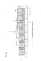
- FIG. 26 Essential components of a third embodiment of this invention are shown in Fig. 26. This embodiment expands on the second embodiment to provide a configuration that can be applied to mass production. Portions that are equivalent to those of the second embodiment are denoted by the same reference numbers.
- the configuration is such that a large number (7, in this figure) of shaping vessels 37 move along graphite rails 50 at a low speed (in this case: 300 mm/H) from right to left.
- a linear shaft is driven by a motor, not shown in the figure, so that the shaping vessel at the right-hand end is pushed at a low speed by this linear shaft.
- a mechanism is provided to load the shaping vessels 37 one at a time onto a right-hand end portion of the rails and remove these shaping vessels 37 one at a time from a left-hand end portion of the rails 50.
- the heater 35 is disposed around the path along which the shaping vessels 37 move (but is shown only thereabove in the figure).
- Raw crystal material 42 is contained in the base portion of the shaping vessel 37 at the right-hand end.
- the raw crystal material 42 is subjected to strong heating from the heater 35 as it moves along the rails 50 from right to left and, when it passes its melting point, it becomes the melt 43.
- the shaper 38 is pressed downward by the pressuring member 39 at substantially the center of the movement path thereof, so that the melt 43 is injected into the gaps formed in the shaper 38.
- the melt 43 injected into the gaps of the shaper 38 are subjected to weaker heating as it moves away from the center of the movement path, and gradually solidifies from the lower left-hand side to form the crystal 44.
- a low-temperature crystal 45 is further formed as the movement continues to the left. If it is assumed that the width of the shaping vessels 37 in Fig.
- the operation speed is 300 mm/H
- the pressuring member 39 presses the shaper 38 at a rate of twice per hour.
- the present invention can also be applied to the fabrication of semiconductor crystals such as silicon crystals and gallium/antimony crystals, fluoride crystals, oxide crystals, or metal crystals.
- semiconductor crystals such as silicon crystals and gallium/antimony crystals, fluoride crystals, oxide crystals, or metal crystals.
- the description of the above embodiment related to the fabrication of needle or sheet crystals the present invention can be applied to the fabrication of other shapes of crystal, by changing the form of the shaper.
- the method of fabricating a shaped crystal in accordance with this invention is useful for fabricating various kinds of crystals such as bismuth/tellurium compound thermoelectric semiconductor crystals, silicon crystals, or germanium crystals, and is particularly suitable for the fabrication of a large number of highly functional monocrystals in batches.
Landscapes
- Chemical & Material Sciences (AREA)
- Engineering & Computer Science (AREA)
- Crystallography & Structural Chemistry (AREA)
- Materials Engineering (AREA)
- Metallurgy (AREA)
- Organic Chemistry (AREA)
- Inorganic Chemistry (AREA)
- Manufacturing & Machinery (AREA)
- Cooling Or The Like Of Semiconductors Or Solid State Devices (AREA)
- Crystals, And After-Treatments Of Crystals (AREA)
- Liquid Deposition Of Substances Of Which Semiconductor Devices Are Composed (AREA)
- Control Of Temperature (AREA)
Applications Claiming Priority (5)
| Application Number | Priority Date | Filing Date | Title |
|---|---|---|---|
| JP27675195 | 1995-09-29 | ||
| JP27675195A JP3151759B2 (ja) | 1994-12-22 | 1995-09-29 | 熱電半導体針状結晶及び熱電半導体素子の製造方法 |
| JP7351521A JPH09181362A (ja) | 1995-12-26 | 1995-12-26 | 可撓性を有する熱電素子及びそれからなる冷却加熱装置 |
| JP35152195 | 1995-12-26 | ||
| EP96925133A EP0795630B1 (fr) | 1995-09-29 | 1996-07-30 | Procede pour fabriquer des cristaux formes par une injection de liquide avec pression verticale |
Related Parent Applications (1)
| Application Number | Title | Priority Date | Filing Date |
|---|---|---|---|
| EP96925133A Division EP0795630B1 (fr) | 1995-09-29 | 1996-07-30 | Procede pour fabriquer des cristaux formes par une injection de liquide avec pression verticale |
Publications (1)
| Publication Number | Publication Date |
|---|---|
| EP1329538A2 true EP1329538A2 (fr) | 2003-07-23 |
Family
ID=26552099
Family Applications (3)
| Application Number | Title | Priority Date | Filing Date |
|---|---|---|---|
| EP96925133A Expired - Lifetime EP0795630B1 (fr) | 1995-09-29 | 1996-07-30 | Procede pour fabriquer des cristaux formes par une injection de liquide avec pression verticale |
| EP03007764A Withdrawn EP1329538A2 (fr) | 1995-09-29 | 1996-07-30 | Procédé pour fabriquer des cristaux formés par une injection vers le haut de liquide sous pression |
| EP96925134A Expired - Lifetime EP0805501B1 (fr) | 1995-09-29 | 1996-07-30 | Dispositif thermoelectrique et refroidisseur/chauffeur thermoelectrique |
Family Applications Before (1)
| Application Number | Title | Priority Date | Filing Date |
|---|---|---|---|
| EP96925133A Expired - Lifetime EP0795630B1 (fr) | 1995-09-29 | 1996-07-30 | Procede pour fabriquer des cristaux formes par une injection de liquide avec pression verticale |
Family Applications After (1)
| Application Number | Title | Priority Date | Filing Date |
|---|---|---|---|
| EP96925134A Expired - Lifetime EP0805501B1 (fr) | 1995-09-29 | 1996-07-30 | Dispositif thermoelectrique et refroidisseur/chauffeur thermoelectrique |
Country Status (4)
| Country | Link |
|---|---|
| US (2) | US5885345A (fr) |
| EP (3) | EP0795630B1 (fr) |
| DE (2) | DE69627299T2 (fr) |
| WO (2) | WO1997013284A1 (fr) |
Cited By (1)
| Publication number | Priority date | Publication date | Assignee | Title |
|---|---|---|---|---|
| FR2918080A1 (fr) * | 2007-06-29 | 2009-01-02 | Commissariat Energie Atomique | Dispositif et procede d'elaboration de plaquettes en materiau semi-conducteur par moulage et cristallisation dirigee |
Families Citing this family (59)
| Publication number | Priority date | Publication date | Assignee | Title |
|---|---|---|---|---|
| JPH10178216A (ja) * | 1996-12-18 | 1998-06-30 | Seru Appl Kk | 熱電素子及び熱電冷却装置 |
| US6458319B1 (en) * | 1997-03-18 | 2002-10-01 | California Institute Of Technology | High performance P-type thermoelectric materials and methods of preparation |
| JP3255629B2 (ja) | 1999-11-26 | 2002-02-12 | モリックス株式会社 | 熱電素子 |
| US6440212B1 (en) * | 2000-02-28 | 2002-08-27 | Microfab Technologies, Inc. | Low cost method for making thermoelectric coolers |
| DE10045419B4 (de) * | 2000-09-14 | 2007-12-20 | Fraunhofer-Gesellschaft zur Förderung der angewandten Forschung e.V. | Verfahren zur Herstellung eines thermoelektrischen Bauelements, thermoelektrisches Bauelement sowie Vorrichtung zur Durchführung des Verfahrens |
| JP2004534386A (ja) | 2001-04-09 | 2004-11-11 | リサーチ・トライアングル・インスティチュート | Dnaゲノムチップ、プロテオームチップ、熱光スイッチング回路および赤外線タグ用薄膜熱電加熱冷却装置 |
| US6410971B1 (en) | 2001-07-12 | 2002-06-25 | Ferrotec (Usa) Corporation | Thermoelectric module with thin film substrates |
| CN1326205C (zh) * | 2001-07-25 | 2007-07-11 | 精工爱普生株式会社 | 半导体薄膜及半导体装置的制造方法、半导体装置、集成电路、电光学装置及电子机器 |
| US7342169B2 (en) | 2001-10-05 | 2008-03-11 | Nextreme Thermal Solutions | Phonon-blocking, electron-transmitting low-dimensional structures |
| US6700052B2 (en) * | 2001-11-05 | 2004-03-02 | Amerigon Incorporated | Flexible thermoelectric circuit |
| US20040178517A9 (en) * | 2001-12-21 | 2004-09-16 | Siu Wing Ming | Split body peltier device for cooling and power generation applications |
| AU2003230920A1 (en) | 2002-04-15 | 2003-11-03 | Nextreme Thermal Solutions, Inc. | Thermoelectric device utilizing double-sided peltier junctions and method of making the device |
| DE10230080B4 (de) * | 2002-06-27 | 2008-12-24 | Fraunhofer-Gesellschaft zur Förderung der angewandten Forschung e.V. | Verfahren zur Herstellung einer thermoelektrischen Schichtenstruktur und Bauelemente mit einer thermoelektrischen Schichtenstruktur |
| CN100427850C (zh) * | 2002-08-07 | 2008-10-22 | 菲尼克斯咨询有限公司 | 调温穿戴物 |
| WO2004105146A1 (fr) * | 2003-05-23 | 2004-12-02 | Koninklijke Philips Electronics N.V. | Procede de fabrication d'un dispositif thermoelectrique et dispositif thermoelectrique obtenu selon ce procede |
| US7638705B2 (en) | 2003-12-11 | 2009-12-29 | Nextreme Thermal Solutions, Inc. | Thermoelectric generators for solar conversion and related systems and methods |
| JP4521236B2 (ja) * | 2004-08-31 | 2010-08-11 | 株式会社東芝 | 熱電変換装置及び熱電変換装置の製造方法 |
| US7523617B2 (en) | 2004-10-22 | 2009-04-28 | Nextreme Thermal Solutions, Inc. | Thin film thermoelectric devices for hot-spot thermal management in microprocessors and other electronics |
| US7587901B2 (en) | 2004-12-20 | 2009-09-15 | Amerigon Incorporated | Control system for thermal module in vehicle |
| JP2006287066A (ja) * | 2005-04-01 | 2006-10-19 | Denso Corp | 熱電変換装置およびその装置の製造方法 |
| US8623687B2 (en) | 2005-06-22 | 2014-01-07 | Nextreme Thermal Solutions, Inc. | Methods of forming thermoelectric devices including conductive posts and/or different solder materials and related methods and structures |
| WO2007002342A2 (fr) | 2005-06-22 | 2007-01-04 | Nextreme Thermal Solutions | Procédés de fabrication de dispositifs thermoélectriques comprenant des matrices électriquement isolantes entre les traces conductrices et structures associées |
| CN1943918B (zh) * | 2005-08-25 | 2012-07-25 | 雅马哈株式会社 | 制备热电材料、形成热电器件和制造热电模块的方法 |
| US20070101737A1 (en) | 2005-11-09 | 2007-05-10 | Masao Akei | Refrigeration system including thermoelectric heat recovery and actuation |
| US7310953B2 (en) | 2005-11-09 | 2007-12-25 | Emerson Climate Technologies, Inc. | Refrigeration system including thermoelectric module |
| WO2007103249A2 (fr) | 2006-03-03 | 2007-09-13 | Nextreme Thermal Solutions | Procédés de formation de dispositifs thermoélectriques faisant appel à des îlots de matériau thermoélectrique, et structures associées |
| US8222511B2 (en) | 2006-08-03 | 2012-07-17 | Gentherm | Thermoelectric device |
| US7338027B1 (en) * | 2006-08-22 | 2008-03-04 | Cameron International Corporation | Fluid saving blowout preventer operator system |
| US20080087316A1 (en) | 2006-10-12 | 2008-04-17 | Masa Inaba | Thermoelectric device with internal sensor |
| TWI338390B (en) * | 2007-07-12 | 2011-03-01 | Ind Tech Res Inst | Flexible thermoelectric device and manufacturing method thereof |
| US9105809B2 (en) | 2007-07-23 | 2015-08-11 | Gentherm Incorporated | Segmented thermoelectric device |
| US7877827B2 (en) | 2007-09-10 | 2011-02-01 | Amerigon Incorporated | Operational control schemes for ventilated seat or bed assemblies |
| KR101779870B1 (ko) | 2008-02-01 | 2017-10-10 | 젠썸 인코포레이티드 | 열전 소자용 응결 센서 및 습도 센서 |
| JP5997899B2 (ja) | 2008-07-18 | 2016-09-28 | ジェンサーム インコーポレイテッドGentherm Incorporated | 空調されるベッドアセンブリ |
| US8487177B2 (en) * | 2010-02-27 | 2013-07-16 | The Boeing Company | Integrated thermoelectric honeycomb core and method |
| US9601677B2 (en) | 2010-03-15 | 2017-03-21 | Laird Durham, Inc. | Thermoelectric (TE) devices/structures including thermoelectric elements with exposed major surfaces |
| JP5656295B2 (ja) | 2011-04-22 | 2015-01-21 | パナソニックIpマネジメント株式会社 | 熱電変換モジュールとその製造方法 |
| RU2482403C1 (ru) * | 2011-09-02 | 2013-05-20 | Общество с ограниченной ответственностью "Системы связи и технического контроля" (ООО "Системы СТК") | Теплообменник термоэлектрических устройств нагрева-охлаждения |
| WO2013052823A1 (fr) | 2011-10-07 | 2013-04-11 | Gentherm Incorporated | Commandes de dispositif thermoélectrique et procédés associés |
| JP5956155B2 (ja) * | 2012-01-05 | 2016-07-27 | フタバ産業株式会社 | 熱電発電装置 |
| US9989267B2 (en) | 2012-02-10 | 2018-06-05 | Gentherm Incorporated | Moisture abatement in heating operation of climate controlled systems |
| US8397518B1 (en) | 2012-02-20 | 2013-03-19 | Dhama Innovations PVT. Ltd. | Apparel with integral heating and cooling device |
| WO2013129057A1 (fr) * | 2012-02-27 | 2013-09-06 | 株式会社Kelk | Module thermoélectrique, appareil de génération d'énergie thermoélectrique, et générateur d'énergie thermoélectrique |
| JP5670989B2 (ja) * | 2012-11-20 | 2015-02-18 | アイシン高丘株式会社 | 熱電モジュールの製造方法 |
| US9352997B2 (en) * | 2013-06-27 | 2016-05-31 | Nachi-Fujikoshi Corp. | Melt molding method of germanium |
| US9662962B2 (en) | 2013-11-05 | 2017-05-30 | Gentherm Incorporated | Vehicle headliner assembly for zonal comfort |
| KR102252584B1 (ko) | 2014-02-14 | 2021-05-14 | 젠썸 인코포레이티드 | 전도식 대류식 기온 제어 조립체 |
| US11857004B2 (en) | 2014-11-14 | 2024-01-02 | Gentherm Incorporated | Heating and cooling technologies |
| US11033058B2 (en) | 2014-11-14 | 2021-06-15 | Gentherm Incorporated | Heating and cooling technologies |
| US11639816B2 (en) | 2014-11-14 | 2023-05-02 | Gentherm Incorporated | Heating and cooling technologies including temperature regulating pad wrap and technologies with liquid system |
| US11152556B2 (en) | 2017-07-29 | 2021-10-19 | Nanohmics, Inc. | Flexible and conformable thermoelectric compositions |
| US11223004B2 (en) | 2018-07-30 | 2022-01-11 | Gentherm Incorporated | Thermoelectric device having a polymeric coating |
| US12178130B2 (en) * | 2018-11-20 | 2024-12-24 | The Regents Of The University Of California | Flexible thermoelectric devices |
| CN121230238A (zh) | 2018-11-30 | 2025-12-30 | 金瑟姆股份公司 | 热电调节系统和方法 |
| US11152557B2 (en) | 2019-02-20 | 2021-10-19 | Gentherm Incorporated | Thermoelectric module with integrated printed circuit board |
| US20210059854A1 (en) * | 2019-09-03 | 2021-03-04 | Purdue Research Foundation | Portable Thermal Therapy System |
| US12611909B2 (en) | 2021-03-18 | 2026-04-28 | Gentherm Incorporated | Preconditioning surfaces using intelligent thermal effectors |
| US12552223B2 (en) | 2021-03-18 | 2026-02-17 | Gentherm Incorporated | Optimal control of convective thermal devices |
| US20250216126A1 (en) * | 2023-12-27 | 2025-07-03 | Faizan Ahmed | Thermoelectric system consisting of alternating trapezoid elements with increased figure of merit |
Family Cites Families (28)
| Publication number | Priority date | Publication date | Assignee | Title |
|---|---|---|---|---|
| US2815303A (en) * | 1953-07-24 | 1957-12-03 | Raythcon Mfg Company | Method of making junction single crystals |
| JPS34595B1 (fr) * | 1956-12-28 | 1959-02-10 | ||
| JPS3724548Y1 (fr) * | 1960-03-07 | 1962-09-17 | ||
| FR1323569A (fr) * | 1962-02-13 | 1963-04-12 | Thomson Houston Comp Francaise | Perfectionnements aux dispositifs de refroidissement thermoélectriques |
| US3240628A (en) * | 1962-06-14 | 1966-03-15 | Carrier Corp | Thermoelectric panel |
| JPS3827922Y1 (fr) * | 1962-11-30 | 1963-12-20 | ||
| JPS4023300Y1 (fr) * | 1964-02-03 | 1965-08-10 | ||
| JPS5117972B2 (fr) * | 1971-09-01 | 1976-06-07 | ||
| JPS4832942B1 (fr) * | 1971-12-16 | 1973-10-09 | ||
| JPS5120097A (ja) * | 1974-08-09 | 1976-02-17 | Takumi Sogabe | Maguneshiatanketsushono seizohoho |
| FR2330976A1 (fr) * | 1975-11-05 | 1977-06-03 | Air Ind | Perfectionnements apportes aux installations thermoelectriques |
| FR2509637A1 (fr) * | 1981-07-17 | 1983-01-21 | Commissariat Energie Atomique | Procede de sustentation, de positionnement et de moulage sans contact de masses liquides permettant la solidification en forme de materiaux et application de ce procede a la mise en forme de materiaux en microgravite |
| JPS5858348A (ja) * | 1981-10-05 | 1983-04-06 | 株式会社東洋パイルヒユ−ム管製作所 | 断熱複合板に於ける目地の施工法 |
| JPS5858348U (ja) * | 1981-10-14 | 1983-04-20 | 三菱電機株式会社 | 電子冷却装置 |
| US4459428A (en) * | 1982-04-28 | 1984-07-10 | Energy Conversion Devices, Inc. | Thermoelectric device and method of making same |
| US4540550A (en) * | 1982-10-29 | 1985-09-10 | Westinghouse Electric Corp. | Apparatus for growing crystals |
| US4610754A (en) * | 1982-10-29 | 1986-09-09 | Westinghouse Electric Corp. | Method for growing crystals |
| EP0115711B1 (fr) * | 1983-02-09 | 1986-10-08 | Commissariat à l'Energie Atomique | Procédé de préparation de plaques d'un matériau métallique ou semi-métallique par moulage sans contact direct avec les parois du moule |
| US4497973A (en) * | 1983-02-28 | 1985-02-05 | Ecd-Anr Energy Conversion Company | Thermoelectric device exhibiting decreased stress |
| JPS6070720A (ja) * | 1983-09-27 | 1985-04-22 | Toshiba Corp | シリコン薄体製造装置 |
| JPS6215842A (ja) * | 1985-07-12 | 1987-01-24 | Fujitsu Ltd | 電子装置の冷却構造 |
| US4907060A (en) * | 1987-06-02 | 1990-03-06 | Nelson John L | Encapsulated thermoelectric heat pump and method of manufacture |
| JPH01115812A (ja) * | 1987-10-28 | 1989-05-09 | Nippon Sheet Glass Co Ltd | シリコン薄板の製造装置 |
| CN1051242A (zh) * | 1989-10-27 | 1991-05-08 | 吴鸿平 | 复合半导体温差致冷器 |
| JPH0711178Y2 (ja) * | 1990-06-25 | 1995-03-15 | 大同ほくさん株式会社 | 多結晶シリコンシート製造装置におけるシリコン注入圧制御機構 |
| US5031689A (en) * | 1990-07-31 | 1991-07-16 | The United States Of America As Represented By The Administrator Of The National Aeronautics And Space Administration | Flexible thermal apparatus for mounting of thermoelectric cooler |
| JPH07202275A (ja) * | 1993-06-28 | 1995-08-04 | Kiyoshi Yanagimachi | 電子冷却素子の集合体 |
| DE4326662A1 (de) * | 1993-08-09 | 1995-02-23 | Rost Manfred Dr Rer Nat Habil | Flexible Peltierbatterie |
-
1996
- 1996-07-30 EP EP96925133A patent/EP0795630B1/fr not_active Expired - Lifetime
- 1996-07-30 DE DE69627299T patent/DE69627299T2/de not_active Expired - Fee Related
- 1996-07-30 WO PCT/JP1996/002145 patent/WO1997013284A1/fr not_active Ceased
- 1996-07-30 US US08/817,873 patent/US5885345A/en not_active Expired - Fee Related
- 1996-07-30 DE DE69630014T patent/DE69630014T2/de not_active Expired - Fee Related
- 1996-07-30 WO PCT/JP1996/002144 patent/WO1997013010A1/fr not_active Ceased
- 1996-07-30 EP EP03007764A patent/EP1329538A2/fr not_active Withdrawn
- 1996-07-30 US US08/836,746 patent/US6097088A/en not_active Expired - Fee Related
- 1996-07-30 EP EP96925134A patent/EP0805501B1/fr not_active Expired - Lifetime
Cited By (3)
| Publication number | Priority date | Publication date | Assignee | Title |
|---|---|---|---|---|
| FR2918080A1 (fr) * | 2007-06-29 | 2009-01-02 | Commissariat Energie Atomique | Dispositif et procede d'elaboration de plaquettes en materiau semi-conducteur par moulage et cristallisation dirigee |
| EP2014802A1 (fr) * | 2007-06-29 | 2009-01-14 | Commissariat A L'energie Atomique | Procédé d'élaboration de plaquettes en matériau semi-conducteur par moulage et cristillisation dirigée |
| US7601618B2 (en) | 2007-06-29 | 2009-10-13 | Commissariat A L'energie Atomique | Method for producing semi-conditioning material wafers by moulding and directional crystallization |
Also Published As
| Publication number | Publication date |
|---|---|
| DE69627299T2 (de) | 2004-01-29 |
| DE69630014T2 (de) | 2004-06-09 |
| WO1997013010A1 (fr) | 1997-04-10 |
| EP0795630B1 (fr) | 2003-04-09 |
| WO1997013284A1 (fr) | 1997-04-10 |
| EP0795630A1 (fr) | 1997-09-17 |
| EP0805501B1 (fr) | 2003-09-17 |
| EP0795630A4 (fr) | 2000-05-10 |
| US5885345A (en) | 1999-03-23 |
| US6097088A (en) | 2000-08-01 |
| EP0805501A1 (fr) | 1997-11-05 |
| EP0805501A4 (fr) | 1998-09-23 |
| DE69627299D1 (de) | 2003-05-15 |
| DE69630014D1 (de) | 2003-10-23 |
Similar Documents
| Publication | Publication Date | Title |
|---|---|---|
| US5885345A (en) | Method of fabricating shaped crystals by overhead-pressure liquid injection | |
| US4382838A (en) | Novel silicon crystals and process for their preparation | |
| JP5633732B2 (ja) | サファイア単結晶の製造方法およびサファイア単結晶の製造装置 | |
| CA1208525A (fr) | Fabrication de feuilles en materiau semiconducteur de structure cristalline brute a mono-cristalline | |
| CA1155735A (fr) | Methode de fabrication de tiges de silicone | |
| CA1193521A (fr) | Methode et appareil de croissance de semiconducteurs cristallins en feuilles par tirage | |
| US2992903A (en) | Apparatus for growing thin crystals | |
| JP5425421B2 (ja) | モールディングおよび方向性結晶化によって半導体物質のウェハを製造する方法 | |
| JP2009149452A (ja) | 半導体結晶成長方法 | |
| JP2947529B2 (ja) | 整形結晶の製造方法及び製造装置 | |
| JP4693932B1 (ja) | 筒状シリコン結晶体製造方法及びその製造方法で製造される筒状シリコン結晶体 | |
| JP7563058B2 (ja) | 鉄ガリウム合金の単結晶インゴットの加工方法 | |
| US4765863A (en) | Method of preparing a crystalline ingot of Hg1-x.sbsb.o Cdx.sbsb.o Te | |
| JP3513046B2 (ja) | 単結晶の製造装置 | |
| US6497762B1 (en) | Method of fabricating crystal thin plate under micro-gravity environment | |
| JP4292300B2 (ja) | 半導体バルク結晶の作製方法 | |
| JP4549111B2 (ja) | GaAs多結晶の製造炉 | |
| JP7798972B2 (ja) | サファイア棒状体の製造方法 | |
| JP2734820B2 (ja) | 化合物半導体単結晶の製造方法 | |
| JPS63185885A (ja) | 横型結晶成長装置 | |
| JP3647964B2 (ja) | 単結晶基板の製造方法および装置 | |
| JP6400946B2 (ja) | Si‐Ge系固溶体単結晶の製造方法 | |
| CH721280A2 (fr) | Procédé de fabrication de saphir en barre | |
| JPH01126289A (ja) | 化合物半導体単結晶体の製造方法 | |
| JPH04167421A (ja) | 半導体単結晶の製造装置 |
Legal Events
| Date | Code | Title | Description |
|---|---|---|---|
| PUAI | Public reference made under article 153(3) epc to a published international application that has entered the european phase |
Free format text: ORIGINAL CODE: 0009012 |
|
| 17P | Request for examination filed |
Effective date: 20030404 |
|
| AC | Divisional application: reference to earlier application |
Ref document number: 0795630 Country of ref document: EP Kind code of ref document: P |
|
| AK | Designated contracting states |
Designated state(s): DE FR GB |
|
| STAA | Information on the status of an ep patent application or granted ep patent |
Free format text: STATUS: THE APPLICATION HAS BEEN WITHDRAWN |
|
| RAP1 | Party data changed (applicant data changed or rights of an application transferred) |
Owner name: MORIX CO., LTD. Owner name: UNION MATERIAL INC. Owner name: FRIGISTOR TRADING CO., LTD. Owner name: SILICON ENGINEERING LABORATORY LTD. |
|
| 18W | Application withdrawn |
Effective date: 20040624 |