EP1329951A2 - Elektrisch isolierende, thermisch leitende, doppelseitige, vorgehäuste Komponente - Google Patents
Elektrisch isolierende, thermisch leitende, doppelseitige, vorgehäuste Komponente Download PDFInfo
- Publication number
- EP1329951A2 EP1329951A2 EP02080604A EP02080604A EP1329951A2 EP 1329951 A2 EP1329951 A2 EP 1329951A2 EP 02080604 A EP02080604 A EP 02080604A EP 02080604 A EP02080604 A EP 02080604A EP 1329951 A2 EP1329951 A2 EP 1329951A2
- Authority
- EP
- European Patent Office
- Prior art keywords
- component device
- recited
- conductive substrate
- component
- members
- Prior art date
- Legal status (The legal status is an assumption and is not a legal conclusion. Google has not performed a legal analysis and makes no representation as to the accuracy of the status listed.)
- Withdrawn
Links
Images


Classifications
-
- H—ELECTRICITY
- H10—SEMICONDUCTOR DEVICES; ELECTRIC SOLID-STATE DEVICES NOT OTHERWISE PROVIDED FOR
- H10W—GENERIC PACKAGES, INTERCONNECTIONS, CONNECTORS OR OTHER CONSTRUCTIONAL DETAILS OF DEVICES COVERED BY CLASS H10
- H10W90/00—Package configurations
- H10W90/401—Package configurations characterised by multiple insulating or insulated package substrates, interposers or RDLs
-
- H—ELECTRICITY
- H10—SEMICONDUCTOR DEVICES; ELECTRIC SOLID-STATE DEVICES NOT OTHERWISE PROVIDED FOR
- H10W—GENERIC PACKAGES, INTERCONNECTIONS, CONNECTORS OR OTHER CONSTRUCTIONAL DETAILS OF DEVICES COVERED BY CLASS H10
- H10W70/00—Package substrates; Interposers; Redistribution layers [RDL]
- H10W70/20—Conductive package substrates serving as an interconnection, e.g. metal plates
-
- H—ELECTRICITY
- H10—SEMICONDUCTOR DEVICES; ELECTRIC SOLID-STATE DEVICES NOT OTHERWISE PROVIDED FOR
- H10W—GENERIC PACKAGES, INTERCONNECTIONS, CONNECTORS OR OTHER CONSTRUCTIONAL DETAILS OF DEVICES COVERED BY CLASS H10
- H10W70/00—Package substrates; Interposers; Redistribution layers [RDL]
- H10W70/40—Leadframes
- H10W70/479—Leadframes on or in insulating or insulated package substrates, interposers, or redistribution layers
Definitions
- the present invention relates to circuit board components and more particularly to electrically isolated and thermally conductive pre-packaged components.
- a current component used in these applications is a TO247 package.
- These devices utilize metalized ceramic substrates, stamped copper leads or lead frames, wire bonds, or solderable topside integrated circuits (IC).
- IC solderable topside integrated circuits
- solderable topside packages for use with discreet power devices and integrated circuits.
- One of these devices utilizes a plastic material to overmold the TO247 package except for the bottom surface.
- the plastic overmold protects the internal die and wire bonds or bond straps.
- the bottom surfaces in most instances are electrically attached and thermally conductive. It is typically left open to provide a thermal and electrical path out of the package. This path also allows the end user to connect the package to a heat sinking mass or an electrical bus.
- a heat sink pad must be added in order to achieve electrical isolation.
- the pad adds thermal resistance to the assembly, typically on the order of 0.1 to 0.5 degrees per C/watt.
- the TO220-type package is one half the size of a TO247 package.
- the present invention provides an electrically isolated and thermally conductive double-sided TO220-type component.
- the invention provides a pre-packaged component which has particular use in high current and high power applications.
- the component has a pair of ceramic substrates on the top and bottom sides with stamped copper leads or lead frames.
- Integrated circuit (IC) devices such as discrete transistors, diodes, resistors, etc. are positioned between the ceramic substrates.
- Solderable bonded copper layers are provided on the top and bottom ceramic substrates. Power from the device is dissipated in two directions and the temperature rise is reduced approximately in half.
- the electrically isolated top and bottom surfaces eliminate the use of heat sink pads.
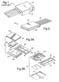
- a known TO220 package component device is shown in Figure 1 and referred to generally by the reference numeral 10.
- the connector 10 has a plastic overmold covering 12, which covers the entire device except for the bottom surface (not shown but referred to by the reference numeral 14).
- the uncovered lower surface can provide a thermal and electrical path out of the package 10. This path also allows the use of a heat sinking mass or an electrical bus. If a heat sink pad is added to achieve electrical isolation, the pad adds thermal resistance to the assembly, typically on the order of 0.1 to 0.5° C/watt.
- TO220 devices are pre-packaged integrated circuit (IC) components for use with printed circuit boards.
- the pre-packaged devices include transistors, diodes, resistors, and other internal components depending on the particular circuit and use desired.
- the leads or lead frame are attached to the circuit boards preferably by soldering.
- Many current TO220-type devices utilize wire leads and wire bonds. Wire bonds crowd or concentrate the current and generate heat. Wire bonds also limit the current density of the device.
- Figure 2 An embodiment of the present invention is shown in Figure 2 and indicated in general by the reference numeral 20.
- Figures 3A and 3B are exploded views of the device 20 showing the components in opposite directions.
- the device 20 has a pair of ceramic substrate members 22 and 24.
- the ceramic material can be any of the ceramic materials commonly used today, but preferably is either alumina (Al 2 O 3 ), aluminum nitride (AIN), silicon nitride (SiN) or beryllium oxide (BeO). These ceramic substrates vary in thermal performance so the selection of the particular ceramic material to be utilized typically depends on the thermal requirements of the specific application.
- the device 20 also includes a lead frame 26, which typically is comprised of a stamped copper material.
- the lead frame typically has a plurality of connector members, including a source member 28, a drain member 30, and a gate member 32.
- the source member, drain member, and gate member are used to connect the device to an electrical bus or other device utilized in the particular application.
- the lead frames are particularly used in high current applications (e.g. 200 ampheres). For lower current applications, individual lead pins can be utilized, as shown in Figures 4A-4B and 5A-5B.
- the device 20 also includes a transistor, such as a MOSFET (metal oxide semiconductor field effect transistor) or an IGBT (isolated gate bipolar transistor) 32 which is positioned between the two substrates 22 and 24 and electrically connected to the members in the lead frame 26.
- a transistor such as a MOSFET (metal oxide semiconductor field effect transistor) or an IGBT (isolated gate bipolar transistor) 32 which is positioned between the two substrates 22 and 24 and electrically connected to the members in the lead frame 26.
- the drain member 30 is soldered and thus mechanically connected to the top and bottom members 22 and 24.
- the drain member 30 is electrically connected to the drain pad 36 only.
- the source member 28 is similarly soldered and mechanically connected to the top and bottom members 22 and 24.
- the source member 28 is electrically connected to the source pad 38 only.
- the gate pin or member 32 is soldered to gate runner 35 which is electrically connected to the gate 34 in the MOSFET.
- Each of the ceramic substrates 22 and 24 can include a layer of solderable material 23 and 25 on the outer surfaces thereof. Pressure attached applications may not require solderable material 23 and 25 on the outer surface. Elimination of 23 and 25 reduces the thermal resistance and device temperature.
- the component device 50 includes upper and lower ceramic substrate members 52 and 54 which have direct bonded copper (DBC) solderable layers 53 and 55, respectively, positioned thereon.
- a pair of source pins 58, a pair of drain pins 60, and a gate pin 62 are positioned between the two substrate members 52 and 54 and protrude therefrom for electrical connection to the IC or bus bar.
- the gate pin 62 electrically connects with gate 64 in the MOSFET 66 by the gate runner 68.
- a pair of ceramic substrate members 82 and 84 is provided in the TO220-type component device shown in Figures 5A and 5B and indicated by the reference numeral 80.
- Each of the substrates has a solderable surface or substrate secured thereon, the substrates being identified by the reference numerals 83 and 85.
- the lead member includes a pair of source pins 86, a pair of drain pins 88, and a gate pin 90. One end of the pins 86, 88, and 90 is positioned between the two substrate members 82 and 84 when the device 80 is assembled and soldered together.
- the device 80 also includes a drain pad 92, which is positioned on ceramic substrate member 84, a MOSFET 94 and a source pad 96 positioned on the ceramic substrate member 82.
- a gate runner 98 connects the gate pin 90 to the gate on the MOSFET 94.
- the MOSFET can have a number of gates, even though only one is used (the others are redundant). The extra gates allow design flexibility, provide the ability to use another gate if the one being utilized were to fail, and allows the device to be self-aligning during assembly.
- the configuration of the lead frame pins, MOSFET, gate runner and the like will change to match the geometry of the integrated circuits utilized with the device.
- power can be dissipated in two directions from the IC component device, either up through the substrate on the upper surface of the device, or down through the base substrate.
- Utilization of a double-sided package reduces the temperature rise of the device approximately in one-half.
- the solderable top and bottom substrates on the device also are isolated from the integrated circuits and pins by the ceramic substrate members. By providing electrically isolated top and bottom surfaces, the use of heat sink pads are eliminated. Heat sink pads are expensive to acquire and utilize in a device and also add thermal resistance to the device on the order of 0.1 to 0.5° C/watt.
- the present invention is not limited to TO220-type devices. It can be used, for example, with devices having larger substrates and "footprints," such as super TO220 devices, TO247 devices and SO devices.
- the invention also has use in both single inline package devices (SIPS) and dual inline package devices (DIPS).
- the present inventive devices have the ability to carry higher currents with less temperature rise than conventional wire bonded and strap bonded devices.
- the inventive devices conduct current and uniformly extract current across the entire face, not just at certain wire bond connection sites.
- the present invention also has better durability and fatigue strength.
- the lower coefficient of expansion results in less movement during temperature cycling leading to longer durability and greater strength.
- lead pins and lead frames also provides for improved processing and manufacturing of the devices.
- the copper lead member can be stamped and plated.
- the assembly can be inline with other high volume hybrid components.
Landscapes
- Cooling Or The Like Of Semiconductors Or Solid State Devices (AREA)
Applications Claiming Priority (2)
| Application Number | Priority Date | Filing Date | Title |
|---|---|---|---|
| US50344 | 2002-01-16 | ||
| US10/050,344 US6812553B2 (en) | 2002-01-16 | 2002-01-16 | Electrically isolated and thermally conductive double-sided pre-packaged component |
Publications (2)
| Publication Number | Publication Date |
|---|---|
| EP1329951A2 true EP1329951A2 (de) | 2003-07-23 |
| EP1329951A3 EP1329951A3 (de) | 2006-03-29 |
Family
ID=21964721
Family Applications (1)
| Application Number | Title | Priority Date | Filing Date |
|---|---|---|---|
| EP02080604A Withdrawn EP1329951A3 (de) | 2002-01-16 | 2002-12-30 | Elektrisch isolierende, thermisch leitende, doppelseitige, vorgehäuste Komponente |
Country Status (2)
| Country | Link |
|---|---|
| US (2) | US6812553B2 (de) |
| EP (1) | EP1329951A3 (de) |
Cited By (2)
| Publication number | Priority date | Publication date | Assignee | Title |
|---|---|---|---|---|
| US10373895B2 (en) | 2016-12-12 | 2019-08-06 | Infineon Technologies Austria Ag | Semiconductor device having die pads with exposed surfaces |
| WO2023030788A1 (de) * | 2021-08-30 | 2023-03-09 | Robert Bosch Gmbh | Elektronikanordnung mit einem leistungshalbleiterbauelement zwischen zwei schaltungsträgern und verfahren zu deren herstellung |
Families Citing this family (35)
| Publication number | Priority date | Publication date | Assignee | Title |
|---|---|---|---|---|
| US7573159B1 (en) | 2001-10-22 | 2009-08-11 | Apple Inc. | Power adapters for powering and/or charging peripheral devices |
| US6812553B2 (en) * | 2002-01-16 | 2004-11-02 | Delphi Technologies, Inc. | Electrically isolated and thermally conductive double-sided pre-packaged component |
| US7148564B2 (en) * | 2004-02-17 | 2006-12-12 | Delphi Technologies, Inc. | Dual-sided substrate integrated circuit package including a leadframe having leads with increased thickness |
| US7538425B2 (en) * | 2004-07-28 | 2009-05-26 | Delphi Technologies, Inc. | Power semiconductor package having integral fluid cooling |
| US7620248B2 (en) * | 2004-11-19 | 2009-11-17 | Microsoft Corporation | System and method for validating graphical components of images |
| US7229855B2 (en) * | 2005-02-23 | 2007-06-12 | Delphi Technologies, Inc. | Process for assembling a double-sided circuit component |
| US7324341B2 (en) * | 2005-09-22 | 2008-01-29 | Delphi Technologies, Inc. | Electronics assembly and heat pipe device |
| US7324342B2 (en) * | 2005-10-19 | 2008-01-29 | Delphi Technologies, Inc. | Electronics assembly and electronics package carrier therefor |
| US7295433B2 (en) * | 2005-10-28 | 2007-11-13 | Delphi Technologies, Inc. | Electronics assembly having multiple side cooling and method |
| US7446401B2 (en) * | 2005-11-02 | 2008-11-04 | Wen-Ping Huang | Structure of power semiconductor with twin metal and ceramic plates |
| DE102005062783A1 (de) * | 2005-12-28 | 2007-07-05 | Robert Bosch Gmbh | Elektronikmodul sowie Verfahren zur Herstellung eines solchen |
| US20070236883A1 (en) * | 2006-04-05 | 2007-10-11 | Javier Ruiz | Electronics assembly having heat sink substrate disposed in cooling vessel |
| US7557434B2 (en) * | 2006-08-29 | 2009-07-07 | Denso Corporation | Power electronic package having two substrates with multiple electronic components |
| US7999369B2 (en) | 2006-08-29 | 2011-08-16 | Denso Corporation | Power electronic package having two substrates with multiple semiconductor chips and electronic components |
| US20090001546A1 (en) | 2007-06-28 | 2009-01-01 | Flederbach Lynda G | Ultra-thick thick film on ceramic substrate |
| US7705436B2 (en) * | 2007-08-06 | 2010-04-27 | Infineon Technologies Ag | Semiconductor device with semiconductor chip and method for producing it |
| DE102007045179A1 (de) * | 2007-09-21 | 2009-04-02 | Robert Bosch Gmbh | Kontaktierungsmodul für Sensor mit begrenztem Bauraum |
| US7875962B2 (en) * | 2007-10-15 | 2011-01-25 | Power Integrations, Inc. | Package for a power semiconductor device |
| US20090309199A1 (en) * | 2008-06-12 | 2009-12-17 | Keith Richard Barkley | Chip package for semiconductor devices |
| US8207455B2 (en) | 2009-07-31 | 2012-06-26 | Power Integrations, Inc. | Power semiconductor package with bottom surface protrusions |
| US20130081845A1 (en) * | 2011-09-30 | 2013-04-04 | Edward Siahaan | Housing for electronic components |
| US8699225B2 (en) | 2012-03-28 | 2014-04-15 | Delphi Technologies, Inc. | Liquid cooled electronics assembly suitable to use electrically conductive coolant |
| US9131630B2 (en) | 2012-03-28 | 2015-09-08 | Delphi Technologies, Inc. | Edge seal for electronics assembly suitable for exposure to electrically conductive coolant |
| EP2814310B1 (de) | 2013-06-14 | 2019-04-17 | Delphi Technologies IP Limited | Kantenabdichtung für Elektronikbaugruppe, die für die Exposition gegenüber elektrisch leitfähigem Kühlmittel geeignet ist |
| US9252512B2 (en) | 2013-08-14 | 2016-02-02 | Hamilton Sundstrand Corporation | Power connector having enhanced thermal conduction characteristics |
| CA2978795A1 (en) | 2015-03-16 | 2016-09-22 | Dana Canada Corporation | Heat exchangers with plates having surface patterns for enhancing flatness and methods for manufacturing same |
| CN108351173B (zh) | 2015-08-27 | 2020-06-30 | 达纳加拿大公司 | 用于双面冷却的热交换器 |
| CN105355614B (zh) * | 2015-11-26 | 2020-09-04 | 国网智能电网研究院 | 一种预封装单芯片及其制备工艺 |
| DE102018204764A1 (de) | 2018-03-28 | 2019-10-02 | Infineon Technologies Ag | Halbleiter- packagesystem |
| JP7306294B2 (ja) | 2020-02-19 | 2023-07-11 | 株式会社デンソー | 半導体モジュール |
| US11967899B2 (en) | 2020-05-22 | 2024-04-23 | Marel Power Solutions | Fluid cooled inverter |
| US12122251B2 (en) | 2022-09-28 | 2024-10-22 | BorgWarner US Technologies LLC | Systems and methods for bidirectional message architecture for inverter for electric vehicle |
| US12526961B2 (en) | 2023-06-07 | 2026-01-13 | BorgWarner US Technologies LLC | Systems for cooling module assembly for inverter for electric vehicle |
| US12528329B2 (en) | 2023-06-07 | 2026-01-20 | BorgWarner US Technologies LLC | Systems for cooling module assembly for inverter for electric vehicle |
| US12461129B2 (en) | 2023-08-28 | 2025-11-04 | BorgWarner US Technologies LLC | Systems and methods for galvanic interface bond detection for inverter for electric vehicle |
Family Cites Families (10)
| Publication number | Priority date | Publication date | Assignee | Title |
|---|---|---|---|---|
| US4538170A (en) * | 1983-01-03 | 1985-08-27 | General Electric Company | Power chip package |
| US4902854A (en) * | 1988-04-12 | 1990-02-20 | Kaufman Lance R | Hermetic direct bond circuit assembly |
| US5340771A (en) * | 1993-03-18 | 1994-08-23 | Lsi Logic Corporation | Techniques for providing high I/O count connections to semiconductor dies |
| US6020636A (en) * | 1997-10-24 | 2000-02-01 | Eni Technologies, Inc. | Kilowatt power transistor |
| US6462413B1 (en) * | 1999-07-22 | 2002-10-08 | Polese Company, Inc. | LDMOS transistor heatsink package assembly and manufacturing method |
| EP2234154B1 (de) * | 2000-04-19 | 2016-03-30 | Denso Corporation | Kühlmittelgekühlte Halbleiteranordnung |
| US6731002B2 (en) * | 2001-05-04 | 2004-05-04 | Ixys Corporation | High frequency power device with a plastic molded package and direct bonded substrate |
| US6670216B2 (en) * | 2001-10-31 | 2003-12-30 | Ixys Corporation | Method for manufacturing a power semiconductor device and direct bonded substrate thereof |
| US6614659B2 (en) * | 2001-12-07 | 2003-09-02 | Delphi Technologies, Inc. | De-mountable, solderless in-line lead module package with interface |
| US6812553B2 (en) * | 2002-01-16 | 2004-11-02 | Delphi Technologies, Inc. | Electrically isolated and thermally conductive double-sided pre-packaged component |
-
2002
- 2002-01-16 US US10/050,344 patent/US6812553B2/en not_active Expired - Lifetime
- 2002-12-30 EP EP02080604A patent/EP1329951A3/de not_active Withdrawn
-
2004
- 2004-09-21 US US10/946,184 patent/US7095098B2/en not_active Expired - Lifetime
Cited By (2)
| Publication number | Priority date | Publication date | Assignee | Title |
|---|---|---|---|---|
| US10373895B2 (en) | 2016-12-12 | 2019-08-06 | Infineon Technologies Austria Ag | Semiconductor device having die pads with exposed surfaces |
| WO2023030788A1 (de) * | 2021-08-30 | 2023-03-09 | Robert Bosch Gmbh | Elektronikanordnung mit einem leistungshalbleiterbauelement zwischen zwei schaltungsträgern und verfahren zu deren herstellung |
Also Published As
| Publication number | Publication date |
|---|---|
| US20030132511A1 (en) | 2003-07-17 |
| US7095098B2 (en) | 2006-08-22 |
| EP1329951A3 (de) | 2006-03-29 |
| US6812553B2 (en) | 2004-11-02 |
| US20050035442A1 (en) | 2005-02-17 |
Similar Documents
| Publication | Publication Date | Title |
|---|---|---|
| US6812553B2 (en) | Electrically isolated and thermally conductive double-sided pre-packaged component | |
| US6946740B2 (en) | High power MCM package | |
| US6723582B2 (en) | Method of making a semiconductor package having exposed metal strap | |
| US7755179B2 (en) | Semiconductor package structure having enhanced thermal dissipation characteristics | |
| US6330158B1 (en) | Semiconductor package having heat sinks and method of fabrication | |
| US7944044B2 (en) | Semiconductor package structure having enhanced thermal dissipation characteristics | |
| US20180233424A1 (en) | Semiconductor package device | |
| EP0700086A2 (de) | Integrierte Schaltungspackung mit verbesserter Wärmesenke | |
| US5796159A (en) | Thermally efficient integrated circuit package | |
| US20080029875A1 (en) | Hermetically sealed semiconductor device module | |
| CN1711639B (zh) | 折叠的柔性无接合引线的多芯片功率封装 | |
| US7229855B2 (en) | Process for assembling a double-sided circuit component | |
| US20040094828A1 (en) | Double-sided multi-chip circuit component | |
| CN101819955B (zh) | 具有增强散热性的半导体封装结构 | |
| EP2017889A2 (de) | Ultradicke Dickfolie auf Keramiksubstrat | |
| US7808088B2 (en) | Semiconductor device with improved high current performance | |
| US20060145312A1 (en) | Dual flat non-leaded semiconductor package | |
| JP7385414B2 (ja) | 半導体装置 | |
| US20240282676A1 (en) | Semiconductor device | |
| US20260068694A1 (en) | Semiconductor Devices and Methods for Manufacturing Thereof | |
| JPS6348850A (ja) | 半導体装置の製造方法 | |
| JPH058944U (ja) | 半導体装置用パツケージ | |
| JPH06334056A (ja) | 半導体装置 | |
| HK1113228B (en) | Semiconductor package structure having enhanced thermal dissipation characteristics | |
| JPH0650353U (ja) | マルチチップモジュールの放熱構造 |
Legal Events
| Date | Code | Title | Description |
|---|---|---|---|
| PUAI | Public reference made under article 153(3) epc to a published international application that has entered the european phase |
Free format text: ORIGINAL CODE: 0009012 |
|
| AK | Designated contracting states |
Designated state(s): AT BE BG CH CY CZ DE DK EE ES FI FR GB GR IE IT LI LU MC NL PT SE SI SK TR |
|
| AX | Request for extension of the european patent |
Extension state: AL LT LV MK RO |
|
| PUAL | Search report despatched |
Free format text: ORIGINAL CODE: 0009013 |
|
| AK | Designated contracting states |
Kind code of ref document: A3 Designated state(s): AT BE BG CH CY CZ DE DK EE ES FI FR GB GR IE IT LI LU MC NL PT SE SI SK TR |
|
| AX | Request for extension of the european patent |
Extension state: AL LT LV MK RO |
|
| RIC1 | Information provided on ipc code assigned before grant |
Ipc: H01L 23/498 20060101ALI20060206BHEP Ipc: H01L 23/492 20060101ALI20060206BHEP Ipc: H01L 23/057 20060101AFI20030409BHEP |
|
| 17P | Request for examination filed |
Effective date: 20060929 |
|
| AKX | Designation fees paid |
Designated state(s): DE FR GB |
|
| 17Q | First examination report despatched |
Effective date: 20090416 |
|
| STAA | Information on the status of an ep patent application or granted ep patent |
Free format text: STATUS: THE APPLICATION IS DEEMED TO BE WITHDRAWN |
|
| 18D | Application deemed to be withdrawn |
Effective date: 20091027 |