EP1333663A2 - Caméra et procédé de prise de vues - Google Patents
Caméra et procédé de prise de vues Download PDFInfo
- Publication number
- EP1333663A2 EP1333663A2 EP03002112A EP03002112A EP1333663A2 EP 1333663 A2 EP1333663 A2 EP 1333663A2 EP 03002112 A EP03002112 A EP 03002112A EP 03002112 A EP03002112 A EP 03002112A EP 1333663 A2 EP1333663 A2 EP 1333663A2
- Authority
- EP
- European Patent Office
- Prior art keywords
- image
- photographing
- data
- pixel
- field
- Prior art date
- Legal status (The legal status is an assumption and is not a legal conclusion. Google has not performed a legal analysis and makes no representation as to the accuracy of the status listed.)
- Granted
Links
- 238000000034 method Methods 0.000 title claims description 49
- 238000012546 transfer Methods 0.000 claims abstract description 292
- 238000012545 processing Methods 0.000 claims abstract description 225
- 238000012937 correction Methods 0.000 claims abstract description 41
- 238000000605 extraction Methods 0.000 claims abstract description 5
- 230000007547 defect Effects 0.000 claims description 129
- 230000015654 memory Effects 0.000 claims description 79
- 238000006243 chemical reaction Methods 0.000 claims description 41
- 230000002950 deficient Effects 0.000 claims description 23
- 230000000295 complement effect Effects 0.000 claims description 16
- 238000003384 imaging method Methods 0.000 claims description 14
- 238000009826 distribution Methods 0.000 claims description 12
- 239000003086 colorant Substances 0.000 claims description 10
- 239000007787 solid Substances 0.000 claims description 10
- 230000000694 effects Effects 0.000 claims description 9
- 230000008569 process Effects 0.000 claims description 9
- 230000010365 information processing Effects 0.000 claims description 5
- 230000008030 elimination Effects 0.000 claims description 2
- 238000003379 elimination reaction Methods 0.000 claims description 2
- 230000002708 enhancing effect Effects 0.000 claims description 2
- 230000000875 corresponding effect Effects 0.000 description 36
- 230000005540 biological transmission Effects 0.000 description 29
- 230000006835 compression Effects 0.000 description 17
- 238000007906 compression Methods 0.000 description 17
- 238000012790 confirmation Methods 0.000 description 16
- 238000001514 detection method Methods 0.000 description 16
- 230000003287 optical effect Effects 0.000 description 12
- 230000004044 response Effects 0.000 description 12
- 238000005070 sampling Methods 0.000 description 10
- 238000003860 storage Methods 0.000 description 10
- 238000010276 construction Methods 0.000 description 9
- 238000010586 diagram Methods 0.000 description 9
- 208000032369 Primary transmission Diseases 0.000 description 7
- 238000000354 decomposition reaction Methods 0.000 description 7
- 239000004973 liquid crystal related substance Substances 0.000 description 7
- 230000001276 controlling effect Effects 0.000 description 5
- 238000001454 recorded image Methods 0.000 description 5
- 208000032370 Secondary transmission Diseases 0.000 description 4
- 230000008859 change Effects 0.000 description 4
- 230000002596 correlated effect Effects 0.000 description 4
- 238000002360 preparation method Methods 0.000 description 4
- 238000010348 incorporation Methods 0.000 description 3
- 238000004519 manufacturing process Methods 0.000 description 3
- 230000000750 progressive effect Effects 0.000 description 3
- 210000003813 thumb Anatomy 0.000 description 3
- 230000015572 biosynthetic process Effects 0.000 description 2
- 239000000470 constituent Substances 0.000 description 2
- 230000006870 function Effects 0.000 description 2
- 230000003068 static effect Effects 0.000 description 2
- WNEODWDFDXWOLU-QHCPKHFHSA-N 3-[3-(hydroxymethyl)-4-[1-methyl-5-[[5-[(2s)-2-methyl-4-(oxetan-3-yl)piperazin-1-yl]pyridin-2-yl]amino]-6-oxopyridin-3-yl]pyridin-2-yl]-7,7-dimethyl-1,2,6,8-tetrahydrocyclopenta[3,4]pyrrolo[3,5-b]pyrazin-4-one Chemical compound C([C@@H](N(CC1)C=2C=NC(NC=3C(N(C)C=C(C=3)C=3C(=C(N4C(C5=CC=6CC(C)(C)CC=6N5CC4)=O)N=CC=3)CO)=O)=CC=2)C)N1C1COC1 WNEODWDFDXWOLU-QHCPKHFHSA-N 0.000 description 1
- 238000009825 accumulation Methods 0.000 description 1
- 230000004888 barrier function Effects 0.000 description 1
- 238000001444 catalytic combustion detection Methods 0.000 description 1
- 230000001413 cellular effect Effects 0.000 description 1
- 239000002131 composite material Substances 0.000 description 1
- 239000000428 dust Substances 0.000 description 1
- 230000004907 flux Effects 0.000 description 1
- 238000005286 illumination Methods 0.000 description 1
- 238000003702 image correction Methods 0.000 description 1
- 230000006872 improvement Effects 0.000 description 1
- 238000011835 investigation Methods 0.000 description 1
- 239000011159 matrix material Substances 0.000 description 1
- 238000005259 measurement Methods 0.000 description 1
- 108091008695 photoreceptors Proteins 0.000 description 1
- 238000003908 quality control method Methods 0.000 description 1
- 230000009467 reduction Effects 0.000 description 1
- 239000004065 semiconductor Substances 0.000 description 1
- 238000004904 shortening Methods 0.000 description 1
Images










Classifications
-
- H—ELECTRICITY
- H04—ELECTRIC COMMUNICATION TECHNIQUE
- H04N—PICTORIAL COMMUNICATION, e.g. TELEVISION
- H04N23/00—Cameras or camera modules comprising electronic image sensors; Control thereof
- H04N23/80—Camera processing pipelines; Components thereof
- H04N23/84—Camera processing pipelines; Components thereof for processing colour signals
-
- H—ELECTRICITY
- H04—ELECTRIC COMMUNICATION TECHNIQUE
- H04N—PICTORIAL COMMUNICATION, e.g. TELEVISION
- H04N25/00—Circuitry of solid-state image sensors [SSIS]; Control thereof
- H04N25/10—Circuitry of solid-state image sensors [SSIS]; Control thereof for transforming different wavelengths into image signals
- H04N25/11—Arrangement of colour filter arrays [CFA]; Filter mosaics
- H04N25/13—Arrangement of colour filter arrays [CFA]; Filter mosaics characterised by the spectral characteristics of the filter elements
- H04N25/134—Arrangement of colour filter arrays [CFA]; Filter mosaics characterised by the spectral characteristics of the filter elements based on three different wavelength filter elements
-
- H—ELECTRICITY
- H04—ELECTRIC COMMUNICATION TECHNIQUE
- H04N—PICTORIAL COMMUNICATION, e.g. TELEVISION
- H04N25/00—Circuitry of solid-state image sensors [SSIS]; Control thereof
- H04N25/10—Circuitry of solid-state image sensors [SSIS]; Control thereof for transforming different wavelengths into image signals
- H04N25/11—Arrangement of colour filter arrays [CFA]; Filter mosaics
- H04N25/13—Arrangement of colour filter arrays [CFA]; Filter mosaics characterised by the spectral characteristics of the filter elements
- H04N25/135—Arrangement of colour filter arrays [CFA]; Filter mosaics characterised by the spectral characteristics of the filter elements based on four or more different wavelength filter elements
- H04N25/136—Arrangement of colour filter arrays [CFA]; Filter mosaics characterised by the spectral characteristics of the filter elements based on four or more different wavelength filter elements using complementary colours
-
- H—ELECTRICITY
- H04—ELECTRIC COMMUNICATION TECHNIQUE
- H04N—PICTORIAL COMMUNICATION, e.g. TELEVISION
- H04N25/00—Circuitry of solid-state image sensors [SSIS]; Control thereof
- H04N25/40—Extracting pixel data from image sensors by controlling scanning circuits, e.g. by modifying the number of pixels sampled or to be sampled
- H04N25/44—Extracting pixel data from image sensors by controlling scanning circuits, e.g. by modifying the number of pixels sampled or to be sampled by partially reading an SSIS array
- H04N25/447—Extracting pixel data from image sensors by controlling scanning circuits, e.g. by modifying the number of pixels sampled or to be sampled by partially reading an SSIS array by preserving the colour pattern with or without loss of information
-
- H—ELECTRICITY
- H04—ELECTRIC COMMUNICATION TECHNIQUE
- H04N—PICTORIAL COMMUNICATION, e.g. TELEVISION
- H04N25/00—Circuitry of solid-state image sensors [SSIS]; Control thereof
- H04N25/60—Noise processing, e.g. detecting, correcting, reducing or removing noise
- H04N25/68—Noise processing, e.g. detecting, correcting, reducing or removing noise applied to defects
Definitions
- the present invention relates to a photographing apparatus such as a digital still camera and a photographing method using a photographing device in an interlacing transfer system where upon transferring electric charges stored in a photographing device the total pixels are divided into a plurality of fields, and a color signal comprising at least RGB or YeCyMgG is involved in transfer data in each field.
- the present invention further relates to a dynamical defect involved in a digital still camera constructed with a solid pick-up device such as a CCD and furthermore relates to an image information processing apparatus.
- a cell constituting each pixel of the CCD generates electric charges in response to the rate of received light.
- the amount of electric charges in each cell are read out as the value of pixels, which value of pixels is outputted subsequently from the CCD as image data for a photograph per 1 frame.
- a digital camera disclosed in Japanese Laid-Open Patent Publication No. 2001-285688 operates in both systems of interlace transfer and progressive transfer.
- the interlacing transfer system in the above disclosure provides a high quality image by making use of a single shot mode with a shatter although long processing time is required, while the progressive transfer system ensures high speed by making use of a continuous photographing mode where a signal of a one pixel train is transferred to a plurality of pixel trains without the use of a shutter, although smear might happen.
- preliminary photographing is performed to adjust the rate of exposure to light by making use of the divided one field in an interlace transfer system, and then to adjust a focused position.
- a CCD for use in a photographing apparatus includes as illustrated in FIG. 38 a pixel S arranged in a matrix, a vertical transfer register VR provided for each vertical line along a horizontal one side of each pixel S, and a horizontal transfer register HR provided on the side of a final end of each vertical transfer register VR.
- any one among three primary filters of R (red), G (green), and B (blue) is disposed on each pixel S.
- the pixel S on which the R filter is disposed converts the light of R and outputs an R signal
- a pixel S on which a G filter is disposed converts the light of B and outputs a G signal
- a pixel S on which a B filter is disposed converts the light of B and outputs a B signal.
- regions from which the respective signals are outputted are arranged horizontally in the order of R,G,R,G...or G,B,G,B, and a horizontal line (hereinafter referred to as an RG line)of the arrangement of the color filters of R,G,R,G...and a horizontal line (hereinafter referred to as a GB line) of the arrangement of the color filters of G,B,G,B... are alternately provided.
- an RG line of the arrangement of the color filters of R,G,R,G...and a horizontal line (hereinafter referred to as a GB line) of the arrangement of the color filters of G,B,G,B...
- the field constructed from the GB line contains only the Gb signal and the B signal, while the field constructed from the RG line contains only the R signal and the Gr signal. More specifically, since all kinds of RGB signals are transferred only after the transfer of the two fields is finished, data required for the image processing of RGB cannot be obtained until the transfer of all fields is finished.
- a cell of the CCD constructing each pixel generates electric charges in response to the quantity of received light.
- the quantity of the electric charges in each cell is read as the value of pixels, which value is in turn outputted in succession from the CCD as image data for a photographic image of 1 frame.
- the digital still camera is improved in its miniaturization and in high resolution. This however causes a severe problem of a pixel defect occurring on part of each cell constructing a pixel as the number of such pixels is increased.
- the pixel defect of this kind includes defects called a white defect, a white defect, an in-bright white defect, and a temperature white defect.
- the black defect originates from dust and the like deposited on a light incident surface of a pixel, and the in-bright white defect originates a defect on a color filter or a micro-lens disposed on the light incident surface.
- any of these black defect and in-bright white defect is a static defect happening irrespective of an operation temperature environment of a CCD, which is being improved as a technique of the manufacture of a semiconductor for use in the manufacturing process of a CCD.
- the temperature white defect is also called a dark current defect, which is a dynamical one influenced by a change in a dark current and accumulation of electric charges, i.e., a change in the temperature of a CCD and a change in exposure time to light.
- Japanese Laid-Open Patent Publication No. 2000-10192 or No. 2000-224487 proposes a technique wherein an address of a pixel where the temperature white defect of a CCD occurs is previously stored in a memory, and the value of a defective pixel is corrected on the basis of an address stored in the memory upon photographing with a digital still camera.
- the temperature white defect changes owing to temperature and exposure time to light, so that for obtaining the address of a pixel on which the temperature white defect occurs it is necessary to take temperature and exposure time to light as parameters, and investigate on which pixel a temperature white defect of a level causing a problem under the conditions of those parameters, and prepare an address table thereof.
- a photographing apparatus is known as an electronic still camera in which electric charges of all pixels accumulated in response to an image focused with imaging means are transferred to a photographing device equipped with color filters for color decomposition, and predetermined image processing is executed to form an image, and which is being assembled as part of functions of a portable information terminal such as a cellular phone and a computer apparatus.
- a photographing device in an interlacing transfer system in which upon electric charges of all stored pixels being transferred data transfer of the electric charges is executed, divided into a plurality of fields" to deal with an increase of the number of pixels and a requirement of making the device compact.
- color filters for color decomposition are of a primary color system of red (R), green (G), and blue (B)
- information involved in one field is red (R) ⁇ green (G) information or blue (B)
- the image processing time requires a predetermined time irrespective of set resolution and a compression rate, which causes a problem of "inconvenience” where even when an object originally requiring less image information such as “images for low resolution and for high compression rate", much time is required until the next photographing is enabled.
- an object of the present invention to provide a photographing device and a photographing method capable of solving the aforementioned problems.
- a photographing apparatus of interlace transferring type comprises:
- a photographing apparatus of interlace transferring type comprises:
- the color filter provided in the photographing device is composed of original color of RGB.
- the color filter provided in the photographing device is composed of complementary color of YeCyMgG.
- the apparatus has an interlace (or interlacing) transfer in which transfers of 3 times carried out by dividing the plurality of fields are achieved and each field is thinned perpendicularly into 1/3.
- the characteristic data of image is color distribution for control of white balance and control value for white balance is generated based on said characteristic.
- the characteristic data of image is also data in which edge component within a screen is extracted and a control value for enhancing the edge is generated based on the characteristic data.
- the characteristic data of image is data in which a color information within a screen is extracted and a control value of color converting coefficient is generated based on said characteristic data.
- the characteristic data of image is data in which distribution of brightness within a screen is extracted and a control value of contrast correction is generated based on said characteristic data.
- the photographing apparatus generates processes image of digitalization and said characteristic data of image is data in which distribution of brightness within a screen is extracted and threshold of digitalized processing based on said characteristic data is generated as a control value.
- an photographing method of interlace transferring type comprises the steps of:
- the present invention provides an photographing method of interlace transferring type comprising the steps of:
- Transfers of 3 times of electrification are carried out by dividing into the plurality of fields and thinning perpendicularly each field into 1/3.
- the photographing apparatus includes a solid photographing device which has a plurality of pixels compartmentalized in every predetermined regions and in which a pixel for detecting a pixel value of each color of three original colors through a color filter of said plurality of pixels is arranged in said regions.
- the photographing device is determined so that a defecting pixel for generating a white scratch of temperature which changes according to temperature is one or less in each region, each pixel value of all the pixels in the solid photographing device being read out with division of fields of three or more to form an image of one frame based on the read out pixel value.
- the apparatus comprises:
- the pixel value of said one pixel is rewritten by the pixel value of the other pixel.
- the apparatus further comprises means for obtaining a difference between a predicated value predicated by a pixel value of each pixel of a third field from each pixel of the first and second fields and a pixel value obtained from each pixel of the third field, and means for judging that when the difference obtained by the said means for obtaining the difference exceeds said predetermined threshold, the pixel of the third field is said defective pixel and for rewriting the pixel value of the defective pixel by said predicated value.
- the photographing mode is a continuous taking-out mode.
- a correcting device for defect of ordinary temperature is provided at prior to said correcting device for white defect of temperature.
- the correcting device for defect of ordinary temperature amending a defect of ordinary temperature which does not depend on temperature of said pixel previously to effect amendment of the pixel value of the defective pixel by said correcting device for white defect.
- a photographing method comprises the steps of:
- a photographing method comprises the steps of:
- An image for confirming photographing is made by image processing including YUV conversion.
- a thumbnail image is made by image processing including YUV conversion.
- Condition of an image to be formed is set and image processing is carried out by use of transfer data of n (m ⁇ n ⁇ M) field to make said image to be formed.
- Condition of an image to be formed is resolution of image and n is number of field in which number of pixel necessary to make an image of the set resolution is get.
- Condition of an image to be formed is compressibility of image, and n is number of field in which number of pixel necessary to make the image of the set compressibility is get.
- an photographing apparatus comprising:
- the color filter of the photographing device is composed of original colors of red (R), green (G) and blue (B).
- the color filter of the photographing device is composed of complementary color of yellow (Y), cyan (C), magenta (M) and green (G).
- M is 3 in the photographing device of interlace transferring type, and said apparatus embodies said photographing method as recited in claim 29 or 34.
- M is 4 or 6 in the photographing device of interlace transferring type, and said apparatus embodies said photographing method as recited in claim 30, 31 or 34.
- the apparatus can embodies the photographing method and has a displaying part for displaying an image for confirming pick up and/or an image of thumbnail.
- the apparatus has also a removable exterior memory for storing the formed image.
- the apparatus has an image holding section for storing the formed image.
- An information processing apparatus of image comprising said photographing apparatus is also provided.
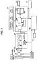
- FIG. 1 a block diagram illustrating the construction of a digital camera including a photographing apparatus in a preferred embodiment of the first invention is provided.
- the preferred embodiment exhibits as an example a photographing apparatus employing a photographing device in a 3: 1 interlacing transfer system containing all RGB signals in each field by dividing electric charges stored in the photographing device to 3 fields upon transferring the electric charges.
- a photographing device (referred hereinafter to as a CCD.) which includes a primary color system RGB color filter and transfers electric charges by dividing them to 3 fields
- 102 is a photographing/processing section (including CSD: Correlated Double Sampling Circuit, AGC (Automatic Gain Control Circuit), A/D (Analog/Digital Converter Circuit), TG (Timing Generation Circuit, etc.), which takes out an image focused on a CCD surface after entering the same surface through a group of photographing lenses and a shutter as an analog image signal and converts it to a digital image signal
- 103 is a signal processing section for executing a processing such as storing a digital image signal in a memory section (SDRAM) 104 through the CCD- I/F 3a , and a memory controller 3b
- 105 is a control section (CPU) for controlling each section
- 106 is a display section for displaying an image for confirming photographing and a thumb-nail image
- 107 is an operation section
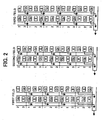
- FIG. 2 a schematic is provided illustrating the transfer of data in CCD, on which there are provided color filters of a primary color system in a 3: 1 interlacing transfer system containing all RGB signals in each field obtained by dividing electric charges stored in the CCD in the present embodiment into 3 fields upon the transfer of those electric charges.
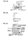
- FIG. 3(a) a front view is provided illustrating an external appearance of the digital camera including the photographing apparatus in the present embodiment, with FIG. 3(b) a side view of the same and FIG. 3(c) an upper surface view of the same.
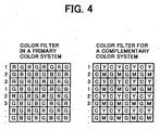
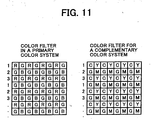
- R, Gr signals and B, Gb signals in the primary system illustrated in FIG. 2 may be replaced by Ye, Cy signals and Mg, G signals in the complementary color system (Refer to FIG. 4.).
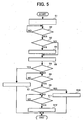
- step S1 data corresponding to the first field among the 3 fields as data of electric charges stored in the CCD lin response to an image being a photographing object is transferred, and the transferred data are stored in the memory section 104 after mediating the photographing processing section 102 and then the CCD-I/F 103a in the signal processing section 3 and the memory controller 103b in step S1. It is confirmed that the transfer of the data in the first field has been completed in step S2, and at the time the data transfer has been completed (Yes in S2) it is confirmed whether or not setting for displaying an image for confirming the photographing is existent in step S3. Since all the data of the RGB signals of a pixel are contained in the data transferred from the first field, the image processing can be executed at the time the transfer has been completed.
- step S5 when the operation is not setting for displaying of the image for confirming the photographing in the processing S3 (No in step S3), or after the finishing of the processing S4, an image processing for preparing a thumb -nail image is executed in step S5. Further, it is confirmed whether or not a resolution of an image to be prepared is set to be "low” in step S6, and when the setting is the "low” resolution (Yes in S6), the image processing is executed using the transfer data in the first field in step S7.
- step S6 When the setting is not the "low” resolution (No in step S6), it is confirmed in step S6 whether or not the transfer of data in the second field has been completed, and further it is confirmed whether or not the resolution of an image to be prepared is set to "middle" in step S9.
- the setting of the resolution is "middle” (Yes in step S9), the image processing is executed using the transfer data in the first and second fields in step S10.
- step S11 when the setting is not the "middle" resolution in S9 (No in S9), it is confirmed in step S11 that data transfer for the third field has been completed, and an image processing providing a high resolution is executed using the transfer data in the first, second, and third fields in step S12.
- the transfer data from the CCD 101 are stored in the memory section 104 (RAW- RGB region) mediating the photographing processing section 102 and the CCDI/F 103a in the signal processing section 103 and the memory controller 103b.
- the data of the RGB signal stored in the memory section 104 (RAWRGB region) through the memory controller 103b owing to the detection of the completion of the transfer of each field in response to the setting of the photographing confirmation image, and "low", “middle”, and “high” of the resolution by a user are converted to the data of the YUV signal by the YUV (brightness color difference signal) conversion section 3c and is again stored in the memory section 104 (YUV region).
- the photographing confirmation image and the thumb -nail image prepared on the basis of the transfer data in the first field are displayed on the display section 106 through the display section I/F 103e.
- the data of the YUV signal is read from the memory section 104, and is subjected to a compression processing into a JPEG format, and is stored in the memory section 104 (JPEG region).
- header data and the like are added to the data subjected to the JPEG compression, and are stored in the external memory section 104' by the control section 105 as the JP'EG image data.
- the image processing is achieved using the transfer data in the first and second fields based upon the detection of the completion of the data transfer in the second field
- the image processing is achieved using the transfer data in the first, second, and third fields based upon the detection of the completion of the data transfer in the third field.
- data with horizontal 2048 pixels and vertical 512 pixels is transferred by the one time transfer.
- VGA horizontal 640 pixels and vertical 480 pixels
- an image can be formed on the basis of the number of transfer pixels in the first field.
- data with horizontal 2048 pixels and vertical 1024 pixels is provided using the number of transfer pixels in the first and second fields (corresponding to 2 times) to form an image with the size of horizontal 1024 pixels and vertical 768 pixels (XGA) and with the size of horizontal 1280 pixels and perpendicular 1024 pixels.
- the aspect ratio can be adjusted by executing a processing such as reading with thinning from the memory section upon the conversion processing in the YUV conversion section.
- a photographed image can be satisfactorily processed with the transfer data in the first field, so that the processing of the data transfer in the first and second fields can be interrupted, and the processing jumps to the next photographing to speed up the processing. More specifically, use is made of transfer data in a field required for an image processing in response to the setting of a resolution, and the next photographing is started without executing data transfer in an unnecessary field.
- transfer data in the first, second, and third fields transferred from the CCD for image processing in response to the setting of a compression ratio. For example, when an image is desired to be recorded and transmitted quickly, a choice is frequently made of a high compression ratio. So, when a high compression ratio is set, image processing is executed using transfer data in the first field, and in a middle compression ratio transfer data in the first and second fields are used and in a low compression ratio transfer data in the first, second, and third fields are used.
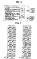
- FIG. 6 there is provided a view exemplarily illustrating a select screen for setting a resolution on a liquid crystal monitor that is a display section of a digital camera.
- a display "off” or display time “1 sec”, “3 sec” are set, and at the item of a recorded image resolution "high”, “middle”, and “low” are inputted and set from an operation section.
- the image compression ratio identical display is achieved and set with the choice of a user.
- the data transfer divided into the three fields was taken as an example, provided that the number of pixels on the photographing device is increased with the transfer time of the number of all pixels being increased from now on, and further the VGA size is obtained from the number of transfer pixels in the divided 1 field, it is also considered that the number of divided fields is increased as in the case where pixels are divided into 5 fields for data transfer.
- a high speed image processing is achieved by selecting an optimum processing in response to the setting of an image output previously set by a user.
- FIG. 8 there is provided a block diagram substantially illustrating the construction of a digital camera including a photographing apparatus in the preferred embodiment of the second invention.
- a photographing apparatus using a photographing device in a 3: 1 interlacing transfer system containing all RGB signals in each field by dividing the electric charges into three fields upon the electric charges stored in the photographing device being transferred.
- a photographing device (hereinafter, simply referred to as a CCD.) in which RGB color filters in a primary color system are provided for transferring electric charges while dividing the transfer 3 times;
- 202 is a photographing/processing apparatus for taking out as an analog image signal an image incident and focused on a CCD surface through a group of photographing lenses and a shutter, and converting it to a digital image signal (including a CSD ( Correlated Double Sampling Circuit), an AGC (Automatic Gain Control Circuit), an A/D ( Analog/Digital Conversion Circuit), and a TG (Timing Generation Circuit), etc.);
- 203 is a signal processing section for storing a digital image signal in a memory section (SDRAM) 204 through a CCD -I/F 203a and executing processing such as extracting characteristic data in an image;
- 205 is a control section (CPU) for generating a control value for use in image correction based upon the extracted characteristic data, and controlling the respective sections.
- SDRAM
- FIG. 9 there is provided a schematic view illustrating the data transfer in the CCD on which there are provided color filters in a primary color system in a 3: 1 interlacing transfer system where upon transferring electric charges stored in the CCD the transfer is divided into 3 fields and all RGB signals are contained in each field, with FIG. 10(a) being a front view illustrating an external appearance of the digital camera including the photographing apparatus in the present embodiment, with FIG. 10(b) a side view, and with FIG. 10(c) an upper view of the same.
- a first field contains all components of the RGB signals.
- the characteristic data of an image formed by transfer data containing all the RGB signals can be obtained after the first field has been transferred.
- the second and third fields are transferred, respectively. Further, it is possible to replace R, Gr signals and B, Gb signals in a primary color system illustrated in FIG. 9 by Ye, Cy signals and Mg, G signals in a complementary color system (see FIG. 11.).
- step S1 As data of electric charges in the CCD 201 stored in response to a photographing object image data transfer corresponding to the first field among the divided three fields is executed in step S1.
- the characteristic data of an image is extracted with the CCD- I/F 203a of the signal processing section 203 through the photographing/processing section 202 and is stored in the memory section 204 in step S2.
- step S4 the data in the third field is transferred in step S4, and after the transfer of all the data in the first to third fields has been finally completed in step S5, the data of the RGB signals stored in the memory section 204 (RAW- RGB region) through the memory controller 203b is converted to the data of the YUV signal through the YUV (brightness color difference signal) conversion section 203c, and is again stored in the memory section 204 (YUV region).
- the time of the conversion use is made of a control value generated in the control section 205 on the basis of the previously extracted characteristic data in step S6.
- the data of the YUV signal is again read from the memory section 204, and is subjected to a compression processing into a JPEG format for example with the compression processing section 203d and is stored ion the memory section 204. Further, upon the data being stored in the memory section 204 (JPEG region) header data, etc., are tagged to the JPEG compressed data into JPEG image data, and is stored in the external memory section 204' with the control section 205 in step S7.
- JPEG region JPEG region
- color distribution data for control which calculates the gain of white balancing, brightness data of a plurality of areas obtained by dividing a screen for use in setting of a contrast where a brightness distribution is made uniform, output data of the image data from a high pass filter for calculating an image edge emphasizing coefficient corresponding to the size of an output signal emphasizing the edge of an image, and further color information of the respective is obtained by dividing a screen into a plurality of the areas.
- a color conversion coefficient where the tone of a skin color is reproduced to a more preferable one is calculated, and an image processing is executed where the YUV conversion using the present color conversion is executed.
- FIG. 13 a block diagram illustrating the substantial construction of a digital camera including the photographing apparatus in the above described embodiment of the present invention is provided. Identical symbols shall be applied to those having identical functions corresponding to constituent members in the embodiment illustrated in FIG. 8.
- a photographing apparatus which employs a photographing device in a 3: 1 interlacing transfer system in which upon transferring electric charges stored in the photographing device the transfer is divided into three fields, each of which fields contains all the RGB signals.
- a CCD 1 is that following a 3: 1 interlacing transfer system in which RGB signals in a primary color system are contained and the transfer is divided into three times.
- the CCD -I/F 203a the foregoing white balance gain adjustment for an image, a contrast set value, an edge emphasizing coefficient, and a color conversion coefficient. More specifically, in the construction where the control value is set in the initial stage of the image processing section 203 the use of the control value prepared from the obtained characteristic data resolves a problem that such a processing as reflecting the prepared control value for the image obtaining the characteristic data is impossible, and assures the processing.
- a photographing apparatus for extracting the characteristic data of an image with the data transfer in the first field, and calculating and setting control values based upon the characteristic data in the course of the data transfer in the second field when image formation is executed on the basis of the data transfer in one field without the use of all pixels corresponding to one frame, for example the image formation is executed using only the third field.
- Electric charges of an image focused on the surface of the CCD 201 are taken out with the CCD 201 as an analog image signal.
- the analog image signal is converted to a digital signal with the photographing/processing section 202 (CDS, AGC, A/D), and is stored in the memory section 204b through the CCD - I/F 203a of the signal processing section 203, and at the time the data transfer through the first field is completed, the YUV conversion is executed for the transfer data through the first field, and further image characteristic data generated upon the conversion is read out by the control section 205.
- the processing is processed in the course of the data transfer through the second field, and a control value is calculated from image characteristic data read in the control section 2905 and is set in the CCD - I/F 203a.
- the control value becomes effective for all the pixels of the transfer data, whereby the control value using image characteristic data of a photographed data can be reflected on a screen for photography.
- the data of the RGB signal through the third field are read out from the memory section (SDRAM) 204, and are YUV-converted in the YUV conversion section 203c, and are JPEG -compressed by the compression processing section 203d, and are stored in the external memory section (memory card) 204' as a JPEG image file.
- SDRAM memory section
- JPEG JPEG -compressed by the compression processing section 203d
- aspect ratios of horizontal and vertical sizes are not coincident with each other, but the aspect ratio can be adjusted by executing reading with thinning from the memory section (SDRAM) 204 upon the transfer to the YUV conversion section 203 for the YUV conversion for example.
- SDRAM memory section
- the characteristic data is extracted in the YUV conversion section 203c
- the characteristic data may be extracted in the CCD-I/F 203a in the same fashion as in the first embodiment, and it is also possible to obtain the characteristic data in the first field, prepare a control value upon the data transfer through the second field and set it to the CCD - I/F 203a, and reflect the control value on the data transfer through the third field.
- a threshold for discriminating a bright portion and a dark portion is previously determined to judge them with the image characteristic data from the transfer data corresponding to the 1 fields.
- a screen is divided into small areas, brightness distribution on which area is detected, and a threshold in each area must be determined.
- the threshold of each area can be calculated before the data transfers in the second and third frames are finished on the basis of the data of the RGB signals written in the memory section (SDRAM) 204 in the data transfer through the first field, and when the data transfer has been finished, the binary processing can be started using the calculated threshold. It is also possible to calculate the threshold using the brightness distribution being the image characteristic data in the first field.
- the characteristic data of an image is obtained on the basis of the transfer data in the first field, and before incorporation of the transfer data in the remaining fields is finished, the calculation of the control value for use in the image processing is started to speed up the image processing.
- the transfer of stored electric charges is divided into three fields, and all color signal components can be obtained with the data transfer in the first field by making used of the photographing device in the 3: 1 interlacing transfer system including all color signals in each field, so that characteristic data of an image over the entire surface of a screen is obtained on the basis of the transfer data, and by starting the calculation of the control value for use in the image processing thereafter, with respect to a range where incorporation of the transfer data in each field is completed the processing can be started before incorporation of the transfer data in the remaining field is completed, to speed up the image processing.
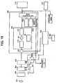
- the digital camera associated with the present invention comprises as illustrated in FIG. 15, a CCD 402 for converting an optical image of an object to be photographed obtained through a photographing lens 401 to an analog electric signal, a CD (&RUUHODWHG' RXEOH 6DPSOLQJ-correlation double sampling) ⁇ A/D circuit 403 including an analog/digital converter for subjecting an analog image signal outputted from the CCD 402 to sample holding and analog/digital conversion successively, a digital signal processing circuit (DSP) 405 including a temperature white defect correction apparatus 404 for correcting any temperature white defect that is one of image defects in the CCD for a digital image signal converted by the CDS ⁇ A/D circuit 403 and a signal processing circuit 405a for applying a predetermined image processing to the corrected digital image signal corrected by the temperature white defect correction apparatus 404, and the like , and an SDRAM 419 for temporarily storing image data.
- DSP digital signal processing circuit
- the CCD 402 being a solid photographing device includes therein color filters as described later. Between the photographing lens 401 and the CCD 402 a mechanical shutter 406 is inserted, which shutter ensures the photographing for a still image in the interlacing type CCS 402. Operations of these constituent sections 402 - 406 are controlled with a control section 409 composed of a microcomputer (MPU). A timing generator TG alters the operation modes with the operation of a release 408 provided on the operation section of the digital still camera.
- MPU microcomputer
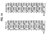
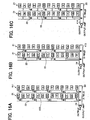
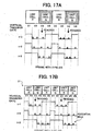
- all the optical detection cells of the CCD i.e., all pixels (Part of there of is illustrated in the figure.) are classified into two fields, as illustrated in FIG. 17 (a).
- the one field is constituted with a group of pixels of any one for each set composed of two pixels adjoining vertically and alternately arranged, while the other field is constituted with the other group of pixels for each set.
- the stored electric charges from the optical detection cells are read to the vertical transfer register for each field with the aid of 4 phase vertical transfer gate signals V1 to V4, and are transferred to the horizontal register following the movement of a potential well constituted with the vertical transfer register.
- all pixels i.e., all the optical detection cell 411(partly illustrated in the figure.) are divided into three fields composed of the group of the pixels of the 3 sets disposed periodically vertically, and fundamentally an image of one frame is constructed with these three fields.
- a filter in an RGB primary color system having such a color arrangement of a zig-zag pattern as illustrated in FIG. 18 for example, which is conventionally well known.
- the color arrangement of the filters in the RGB primary color system illustrated in FIG. 18 (a) includes a color filter corresponding to pixels 411 of 9 x 9 for example obtained when all the pixels 21 of the CCD 402 are defined in a predetermined region.
- a region of the color filter designated at R is a red filter region which arrests transmission of light other than red light
- a region designated at B is a blue filter region which arrests the transmission of light other than blue light
- Gr and Gb indicate a green filter region which arrests the transmission of light other than green light, where the former is a green filter region disposed on a row on which the red filter region is arranged, and the latter is a green filter region disposed on a row on which the blue filter region is arranged.
- the CCD 402 including therein such color filters is manufactured while being subjected to quality control so as to satisfy a prescription that a defective pixel which provides any temperature white defect which might being caused by a dark current of a specified value or more less than 1 in a predetermined region, for example in each region for every 9 x 9 pixels for example, and ones satisfying the specification are available as general commodities. Accordingly, in such a CCD 402 only the existence of only one temperature white defect may be allowed in each the foregoing predetermined region.
- FIG s. 18 (b) to 18 (d) the color arrangement of pixels in each field is extracted, and color arrangements in the A field in FIG. 18(b) and the B field in FIG. 18 (c) are coincident with each other.
- the mechanical shutter 406 In the present process of exposure to light with the operation of the release 408 the mechanical shutter 406 is kept in an open state, and henceforth stored electric charges in response to an optical image of an object to be photographed obtained through the photographing lens 401 are stored in each pixel comprising the optical detection cell 411 of the CCD 402 owing to the present exposure to light.
- the mechanical shutter 406 When the stored electric charges reach a predetermined quantity, the mechanical shutter 406 is closed.
- the stored electric charges are read on the vertical transfer passage 412 (see FIG. 16) in response to a combination of outputs of V1, V3A, B, V5A, B followed by a read pulse as illustrated in FIG. 29 among V1 to V6 being an output of the V driver 410 in a frame read process where the mechanical shutter 406 is in a closed state of the mechanical shutter 406, and a pixel signal corresponding to FIG s. 18 (b) to 18 (d) for each field.
- the outputted image signal undergoes sampling hold ⁇ A/D conversion in the CDS ⁇ A/D circuit 403, and is sent to the temperature white defect correction apparatus 404 as a digital image value.
- the temperature white defect correction apparatus 404 associated with the present invention comprises first and second frame memories 416, 416 each having a memory capacity required for storing a digital pixel value in each field constructed with the pixels 411 of 1/3 of all the pixels 411 of the CCD 402, a subtraction circuit 417, a color interpolation circuit 418, and a control section 419.
- the frame memories 415, 416, the subtraction circuit 417, and the interpolation circuit 418 are controlled by the control section 419. Once a digital value of each pixel in the B field from the sampling hold circuit 403 is outputted with reading of the value of each pixel in the B field on 419. Once the value of each pixel in the A field outputted from the CCD 402 by reading of the value of each pixel in the A field is outputted as a digital value from the CCD 402, the control section 409 stores without correcting an RGB Image value in an external SDRAM 419 and stores in a first frame memory 415, as illustrated in FIG. 19 (b).
- the subtraction circuit 417 subtracts the value (B) of each pixel in the B field from each pixel value in the (A) field stored in the first frame memory 415 with the control of the control section 419 successively.
- the reduction result (A - B) is written in the second frame memory 416 with the control section 409.
- an R value (B field) at third row first column is subtracted from an R value (A field) at first row first column illustrated in FIG. 18 (a), and the result is written in the second frame memory 416, and thereafter respective differences of a Gr value (B field) at 3 rd row 2 nd column from a Gr value (A field) at 1 st row 2 nd column...an R value (B field) at 9 th row 9 th column from an R value (A field) at 7 th row 9 th column are written in the second frame memory 416.
- the control section 409 when the respective subtraction results are compared with a predetermined threshold region, and fall w3ithin the threshold region, judges that no temperature white defect occurs on pixels of one set providing the subtraction result. In contrast, when the subtraction result exceeds the predetermined threshold range, it judges that any temperature white defect occurs on any one among a set of pixels providing the subtraction result. Such judgement is executed for every the foregoing region.
- the judgment on the temperature white defect is ensured for every the foregoing region by properly setting the foregoing threshold range.
- the reason is that the subtraction is executed between pixels located in the vicinity to each other and having the same color, and even if a relatively large difference happens between the values of both pixels with the same color adjoining to each other, the difference is not so large that the temperature white defect occurs, and the existence of only one temperature white defect is allowed in the foregoing region as described previously on the basis of a general manufacturing rule of the CCD 402.
- control section 409 judges whether the temperature white defect happens on any one among a set of pixels providing the subtraction result, the control section 409 further judges whether the subtraction result is positive or negative.
- a positive symbol means that any temperature white defect happens on the pixels in the A field that is the number to be subtracted.
- a negative symbol means that any temperature white defect happens on the pixel in the B field that is the number of subtracting.
- the value of a pixel provided by the temperature white defect indicates a value sharply exceeding the value of a normal pixel.
- the control section 409 once judging, by subtraction between a set of pixels where both fields are existent, that the temperature white defect is existent on a pixel in the one field for example, rewrites the value of a defective pixel in the one field to a value equal to the value of pixels with the same color most adjoining to each other existent in the other field. For example, when a result when the value of R at 3 rd row 1 st column in the B field illustrated in FIG. 18 (b) is subtracted from the value of R at 1 st row 1 st column in the A field illustrated in FIG.
- the value of the defective pixel is corrected as the value of a pixel, and in the external SDRAM 419 there are stored the values of pixels in the A field and B field not containing the temperature white defect.
- the control section 419 erases data in both frame memories 415, 416, whereby the correction process for the temperature white defect about the A field and t5he B field is finished.
- the color interpolation circuit 418 calculates a predicted value D of the value of each pixel in the C field being the third field using the values of pixels in the A field and in the B field not involving the temperature white defect in the external SDRAM 29, and writes in succession the predicted value (D) of each pixel in the first frame memory 415.
- the weighted mean of the values of pixels with the same color as that of pixels located around a pixel to be interpolated or predicted can be adopted.
- the control section 409 stores as illustrated in FIG. 23(d) the read value (C) of each pixel in the C field outputted from the sampling hold circuit 403 in the external SDRAM 419 in succession. Simultaneously, the control section 409 supplies subsequently the read value (D) of each pixel in the C field to the subtraction circuit 417.
- the subtraction circuit 417 once receiving the supply of the read value ( C ) of each pixel in the C field , subtracts the read value ( C ) of each pixel from a predicted value in the frame memory 415.
- the subtraction processing is executed in succession between each pixel of the predicted value D in the read value of each pixel corresponding to the foregoing pixel in the same fashion in the subtraction processing between the A field and the B field.
- the subtraction result (D - C) is written into the second frame memory 416 in succession.
- the predicted value D is considered a value not involving the temperature white defect because it is a value after the correction. Accordingly, provided the temperature white defect is involved in the subtraction result (D - C), it is the case where it is involved in the C field, and in that situation the subtraction result indicates a negative value, and its absolute value exceeds a predetermined threshold. In contrast, provided the temperature white defect is not involved in the C field, the absolute value of the subtraction result (D - C) is not so increased than the case where the temperature white defect is involved in the C field.
- control section 409 once 5he absolute value of the calculation result (D - C) exceeds the threshold for every read value ( C ) of a pixel , judges that the temperature white defect is involved in the value ( C ) of that pixel as a defective pixel.
- the value of the defective pixel corresponding to the C field stored in the external SDRAM 419 is rewritten by a predicted value (D) of a corresponding pixel.
- the data of the value of any pixel undergoes at need by the signal processing circuit 405 a color interpolation processing for improving the resolution of any image, an aperture emphasizing processing for emphasizing the contour of an image, and an RGB - YUV processing for conversion of a color space. Thereafter, the data of the value of any pixel is transferred again to the external SDRAM 419, and properly undergoes the JPEG compression processing with the JPEG compression circuit 405b, and is then stored in a desired recording medium 419'.
- the data of the value of a pixel stored in the external SDRAM 419 forms images of 1 frame using the date of the values of pixels corresponding to all the 3 fields (A, B, C).
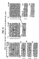
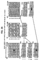
- FIG s. 20 to 28 a view is provided, which exemplarily illustrates a correction processing in the conditions where one temperature white defect is existent for each color of R, G, B for every field (A, B, C) of first to third.
- FIG.20 illustrates a case where temperature white defect ids existent on blue in the A field being the first field.
- FIG.20 there is illustrated an example of the data 420 of the value of a pixel in a color disposition in one region illustrated in FIG.18(a).
- the example 420 of the data of the value of a pixel there is found the value "30" of a pixel located at fourth row 6 th column.
- the value of the pixel is understood to be one concerning blue from the arranged of pixels in FIG.18(a).
- FIG.20 corresponding to FIGs.. 24(b) to FIG.20(d), there are illustrated arranged tables 30a, 30b, and 30-c for the values of pixels extracted from the data 420 of the values of pixels for every field.
- the data table 421 in FIG.20 pixels becoming objects of a subtraction processing by the subtraction circuit 417 concerning then first field (A) and the second field (B) are extracted and listed.
- the calculatioresult (A - B) for each pixel calculated by the subtraction circuit 417 is listed.
- Each value in the data table 421a is a difference between the values of pixels at positions in the arranged corresponding to those on the arranged table 420a and 420b. In the data table 421a they are indicated with "0" excepting one subtractioresult indicating the value of "20".
- the operation result of value [20] means that as explained referring to FIG. 19 (b), there is a defect of a temperature white defect in a pixel for imparting a number to be subtracted, that is, pixel value data 420, a B (blue) pixel of A field positioned on line 4 row 6 of a data table 421.
- a pixel value [30] of the defective pixel is rewritten by a pixel corresponding to the defective pixel, that is, a pixel value [10] of a B pixel positioned on line 6 row 6 to which is imparted a subtraction number of the operation processing, as shown in Data Table 422.
- predication data 422a which is a prediction value D with respect to C field is obtained from each pixel value of A field and B field of Data Table 422 by a color interpolation in a color interpolation circuit 418.
- the subtraction circuit 417 carries out a subtraction with each value of Arrangement Table 420c which is a measured value of C field as a subtraction number, and with each value of the predication data 422a as a number to be subtracted to obtain the subtraction result shown in Data Table 422b.
- Arrangement Table 420c which is a measured value of C field as a subtraction number
- predication data 422a as a number to be subtracted to obtain the subtraction result shown in Data Table 422b.
- all values in Data Table 422b are [0], which therefore means that a temperature white defect is not present in C field. This does not violate the condition, since the present of a temperature white defect has been already found in one B pixel of A field, that the temperature white defect of CCD 402 is not more than one every predetermined area.
- Pixel values of Arrangement Table 420a have been written, when reading C field, in an area of C field of Data Table 422 in FIG. 20, but since the temperature white defect is not contained in each value of C field, the pixel values in C field are not subjected to correction.
- FIG. 21 shows the case where there is a temperature white defect in green of A field.
- a pixel value data example 130 a pixel value [35] is seen in a Gb pixel on line 4 row 5. Therefore, in Data Table 131a showing the operation result (A-B) of Arrangement Tables 130a, 130b is shown a pixel value [20] showing the presence of one temperature while defect.
- this pixel value [20] is positive, it is judged that a temperature while defect is present in a Gb pixel of A field on line 4 row 5 to be a number to be subtracted, and it is rewritten by a pixel value [15] of a Gb pixel in B field position on line 6 row 5 to which is imparted a subtraction number of the operation processing, and Data Table 132 after correction similar to that previously mentioned is obtain within an external SDRRAM 419.
- FIG. 22 shows the case where a temperature white defect is present in red of A field.
- pixel value data 230 a pixel value [25] is obtained in a R pixel on line 7 row 5.
- the pixel value of the R pixel on line 7 row 5 is corrected to [5] by the process similar to that mentioned previously, and Data Table 232 after corrected is obtained in an external SDRAM 419.
- FIGS. 23 to 25 show a treating example where a temperature while defect is present in blue, green and red of B field.
- pixel value data 330 of FIG. 23 a pixel value [30] is seen in a B pixel on line 6 row 4.
- Data Table 331a showing the subtraction result (A-B) of Arrangement Tables 330a, 330b is shown a pixel value [-20] showing the presence of one temperature white defect.
- the pixel value [-20] is negative, it is determined that a temperature white defect is present in a B pixel on line 6 row 4 of B field to be a subtraction number, and it is rewritten by a pixel value [10] of a B pixel of A field positioned on line 4 row 4 to which imparted a number to be subtracted in the operation processing, and a Data Table 332 after correction similar to that described above within an external SDRAM 419 is obtained.
- pixel value data 430 of FIG. 24 a pixel value [30] is seen in a Gb pixel on line 6 row 3.
- Data Table 431a showing the subtraction result (A-B) of Arrangement Tables 430a, 430b is shown a pixel value [-20] showing the presence of one temperature white defect.
- the pixel value of the defect pixel is rewritten by a pixel value [15] of a Gb pixel of A field on line 4 row 3 to which a number to be subtracted is imparted in the subtraction process to obtain a Data Table 432 after correction.
- the pixel value data example of FIG. 25 is an example in which a pixel value [25] is seen in a R pixel on line 3 row 5, the pixel value of the defective pixel is rewritten by a pixel value [5] of a R pixel of A field on line 1 row 5 to which is imparted a number to be subtracted in the operation processing by the processing similar to that explained with reference to FIGS. 23 and 24 to obtain a Data Table 532 after correction.
- FIGS. 26 to 28 show an example in which a temperature white defect is present in a pixel of C field which is a third field.
- pixel value data 630 of FIG. 26 a pixel value [30] is seen in a B pixel on line 8 row 4.
- values of Data Table 631a showing the subtraction result (A-B) of Arrangement Tables 630a, 630b are [0] which represents that a temperature white defect is not present in A field and B field.
- Data Table 631 formed by extracting A field and B field are written in Data Table 632.
- prediction data 632a which is a prediction value D of C field is obtained from values of these A field and B field by a color interpolation circuit 418.
- a subtraction circuit 417 carries out an operation processing (D-C) for subtracting corresponding each value of Arrangement Tale 630c relative to C field from each value of the prediction data 632a.
- D-C operation processing
- Data Table 632b is obtained.
- Data Table 632b is obtained [0] except one operation result showing a value of [-20].
- the operation result means that a temperature white defect is not created as described previously.
- the pixel value [-20] of the defective pixel is rewritten by a prediction value D to which is imparted a number to be subtracted of the above-mentioned operation, that is, a value [10] at an arrangement position of prediction data 632a corresponding to the arranging position of [-20] of Data Table 632b.
- a prediction value D to which is imparted a number to be subtracted of the above-mentioned operation, that is, a value [10] at an arrangement position of prediction data 632a corresponding to the arranging position of [-20] of Data Table 632b.
- pixel value data 730 of FIG. 27 a pixel value [35] is seen in a Cr pixel on line 6 row 4.
- a pixel value shown by a value [-20] of Data Table 732b showing the result of the operation processing (D-C) is rewritten by a value [15] at a corresponding position of Data Table 732a to obtain Data Table 732 in which a temperature white defect is corrected.
- pixel value data 830 of FIG. 28 a pixel value [25] is seen in a R pixel on line 5 row 5 is seen.
- a pixel value shown by a value [-20] of Data Table 832b showing the result of operation processing (D-C) is rewritten by a value [5] at a corresponding position of Data Table 732a to obtain Data Table 832 in which a temperature white defect is corrected.
- FIGS. 20 to 28 showed a pattern in which a differential when a temperature white defect is not created is [0].
- the probability in which a pattern where such a differential is [0] is present is low, and an unevenness occurs also in a pixel value between pixels of the same color free from a temperature white defect.
- that differential is an extremely small value as compared with the case of a temperature white defect as described above, and the aforementioned threshold value range is adequately set to thereby enable determination similar to that explained with reference to FUS, 20 to 28.
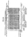
- FIG. 29 shows a timing chart of a digital still camera according to the present invention.
- pixel values of A field, B field and C field obtained after the exposure are subjected to operation processing by a temperature white defect correction device 14, whereby the temperature white defect can be corrected adequately and quickly without necessitating a temperature sensor for detecting a temperature white defect of CCD 402 or address data for a temperature white defect. Accordingly, a good image of one frame without being affected by a temperature white defect can be formed from the corrected pixel values of the three fields within the external SDRAM 419
- a normal temperature defect correction device 407 shown by imaginary lines for correcting a black defect or an in-bright white defect not depending upon the temperature of CCD 402 can be inserted between a sampling signal processing circuit 403 and a temperature white defect correction device 404.
- the normal temperature defect correction device 407 can be also inserted into the rear stage of the temperature white defect correction device 404, but since the influence of the normal temperature defect can be eliminated by correction by means of the temperature white defect correction device 404, it is desirable that the normal temperature defect correction device 407 is inserted into the front stage of the temperature white defect correction device 404.
- FIG. 30 shows a timing chart where an image is formed using a part of pixel values of all pixels of CCD 402.
- FIG. 30 shows an example in which a digital sill came is operated in a serial mode, showing a record mode in pixel number one ninth of all pixels of CCD 402.
- pixel values of A field and B field are subjected to subtraction processing (AB) as explained with reference to FIG, 19 (b) and FIG, 19 (a) and the pixel values of both the field are subjected to correction of a temperature white defect.
- An image in the serial mode is formed using the pixel value of either one of both the fields in which a temperature white defect is corrected.
- the above-described operation processing (A-B) between both the fields is carried out every area, and a pixel representative of a temperature white defect of both the fields can be corrected in any field.
- a pixel value of one field (A or B) which is small in number of temperature white defects is used as a result of the subtraction processing in the whole area for the purpose of enabling quicker image processing, it is desirable that a temperature white defect in the above one field is corrected, and correction is not carried out in the other field but the pixel value of the one field in which correction is made is used to record an image.
- the aforementioned photographing apparatus comprises a photographing device, an imaging means, a photographing processing portion, and an image processing means.
- the photographing device has a color filter for color decomposition.
- the photographing device is means for forming an image to be photographed.
- the imaging means generally has an imaging optical system (a lens system, an imaging mirror system or, a composite system of a lens system and a mirror system or the like), a shutter for passing imaging luminous fluxes through the photographing device or interrupting the same, and a drive portion for driving opening and closing of the shutter,.
- the photographing processing portion carries out the photographing processing for forming a charge accumulated and transferred to the photographing device into a digital signal.
- the image processing means carries out the image processing including at least YUV conversion using transfer data transferred through the photographing processing portion.
- the photographing device is an interlacing transfer system, and in transferring charges of all pixels accumulated, the data transfer of charges is carried out dividing it into M ( ⁇ 3) fields.
- a color filter of the photographing device of the photographing apparatus may be of a primary color system of red (R), green (G) and blue (B), or may be of a complementary color system of yellow (Y), cyan (C), magenta (M) and green (G).
- a pixel value [30] is seen in a B pixel on line 8 row 4.
- values of Data Table 631a showing the subtraction results (A-B) of Arrangement Tables 630a, 630b are [0], indicating that a temperature white defect is not present in A field and B field.
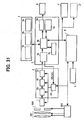
- Fig.31 is a schematic block diagram showing an "electronic still camera (which is normally called a digital camera)" system as another example of the photographing apparatus according to the present invention.
- a “photographing device” indicated at reference character 1 includes a color filter for color decomposition.
- the photographing device is a CCD and the like that utilizes the color filter for the color decomposition
- a series of photographing lenses indicated at reference character 501, a shutter 502, and a driving section 503 constitute "imaging means” for forming an "image to be photographed” on the photographing device 1.
- the driving section 503 is controlled by the controller 5 not only to drivingly open and close the shutter 502, but also to drivingly displace attitude of lenses in the series of photographing lenses in response to an auto-focus (AF) control and a hand-shake correction control.
- AF auto-focus
- a "photographing processor” indicated at reference character 2 performs photographing processing for converting electrical charges which are stored in the photographing device 1 to be transferred, into digital signals.
- the photographing processor 2 includes a CDS (correlated double sampling circuit) 2a, an AGC (automatic gain control circuit) 2b, an A/D (analog/digital conversion circuit) 2c, a TG (timing generation circuit), and the like.
- An "image processor” indicated at reference character 3 includes a CCD-IF (CCD interface) 3a, a memory controller 3b, a YUV converter 3c, a compression processor 3d, and a display I/F (display interface) 3e.
- CCD-IF CCD interface
- memory controller 3b a memory controller
- YUV converter 3c a YUV converter
- compression processor 3d a compression processor
- display I/F display interface
- a “storage section” indicated at reference character 4 is used to store raw data needed for image processing and data subjected to the image processing, and includes a RAW-RGB 4a area for storing the raw data, a YUV area 4b, and a JPEG area 4c.
- the memory of the storage device 4 is volatile.
- an external storage section 4' (for example, a memory card) is attachable and detachable to and from a photographing device body from the outside.
- the external storage section 4' is stored various images generated through the image processing.
- an image holding area 4" may be provided inside the image photographing apparatus in which the above-mentioned various images are stored.
- the memory in the external storage section and the image holding area is also volatile.
- a “controller (CPU)” indicated at reference character 5 controls transmission and reception of data between each section of the image processor 3 and the storage section 4 through the memory controller 3b of the image processor 3. Also, the controller 3 controls the entire photographing apparatus.
- a "display section” indicated at reference character 6 is used to display a thumb-nail image, a photographing confirmation image, and the like.
- An “operating section” indicated at reference character 7 is used to set a photographing condition, a generated image condition, or the like.
- Image processing means for performing the image processing including at least "YUV conversion” using transmission data (comprising digital signals) that are transmitted via the photographing processor 2.
- This image processing means is composed of the image processor 3, the storage section 4, and the controller 5.
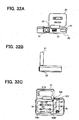
- Fig.32 (a) is a front view; Fig.32 (b) is a side view; and Fig.32 (c) is a top view.
- Reference character 20 denotes a "camera body”, and reference character 21 an "upper lid” attached to freely open and close by a hinge 22 with respect to the camera body 20.
- Fig.32 shows a state with the upper lid 21 opened.
- reference character 501 corresponds to "a series of photographing lenses" as explained with reference to Fig.31, reference character 23 to a "strobe”, and reference character 24 to a "finder".
- reference character 21A denotes a "liquid crystal monitor”
- reference character Sw an "upper-lid opening and closing detection switch”. That is, the upper-lid opening and closing detection switch Sw is a switch for detecting whether the upper lid 21 is open or closed.
- reference character BO denotes a "barrier opening knob”.
- a “date switch” indicated at reference character SD is to perform settings of date and time to the electronic still camera.
- a “frame feeding switch” indicated at reference character SF is a switch for performing frame feeding of the thumb-nail image displayed on the liquid crystal monitor 21A, for example.
- a “storage mode transfer switch” indicated at reference character SM1 is a switch for switching among "recording modes” including a color photographing mode, a monochrome photographing mode, a single-shot mode, a consecutive shot mode, and the like.
- An "image mode switch” indicated at reference character SM2 is a switch for performing settings of a photographed image size and the like.
- Reference character SP denotes a "display switch” for determining whether the display of the image should be performed on the liquid crystal monitor 21A or not, and reference character SE denotes an execution switch (enter switch).
- Reference character SM denotes a "menu switch”.
- reference character RL denotes a "release switch" for performing a shutter operation upon photographing.
- the photographing device 1 is a photographing device that employs an interlacing transfer system in which data transmission of electric charges is carried out by division thereof into M ( ⁇ 3) fields when transferring the electric charges of all pixels stored.
- the photographing device 1 includes the "color filter for color decomposition".
- the color filter may belong to the above-mentioned primary color system, or a complementary color system.
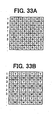
- Fig.33 (a) shows part of a color filter of the primary color system
- Fig.33 (b) shows part of a color filter of the complementary color system.
- R designates a "red filter”, G a "green filter”, and B a "blue filter”.
- These three filters R, G, and B are two-dimensionally arranged as shown in the figure. Looking at the arrangement of these filters in the lateral direction, the R filters and the G filters are alternatively arranged in one line, while the B filters and the G filters are alternatively arranged in the other line. Accordingly, in the entire color filter, the G filter occupies one half of the entire filter, while each of the R and B filters one fourth thereof.
- Y designates a "yellow filter”, G a "cyan filter”, M a “magenta filter”, and G a "green filter”.
- These four filters Y, C, M, and G are two-dimensionally arranged as shown in the figure. Looking at the arrangement of these filters in the lateral direction, the M filters and the G filters are alternatively arranged in one line, while the Y filters and the C filters are alternatively arranged in the other line. Accordingly, in the entire color filter, each filter occupies one fourth of the entire filter.
- the color filter may be employed not only the primary color system but also the complementary color system.
- the primary color system In order to explain the embodiment more concretely, the case of using the primary color system will be described hereinafter with reference to Fig.33 (a).
- R, Gr, Gb, and B designate filters corresponding to the respective pixels.
- pixels of the R filters and pixels of the Gr filters are alternatively arranged in one line
- pixels of the B filters and pixels of the Gb filters are alternatively arranged in the other line.
- the Gr filter is a green filter disposed on an arrangement line of the filter R
- the Gb filter is a green filter disposed on an arrangement line of the filter B.
- the pixels are arranged to be divided into three groups in the longitudinal direction of the figure (namely, in the vertical direction). That is, on the left side of the each pixel, numbers 1, 2, and 3 are repeatedly recorded in the vertical direction. Each number corresponds to one line of the pixel arrangement in the horizontal direction. Such a line of the pixel arrangement in the horizontal direction is a "field". Theses fields are classified by the numbers disposed on the respective left sides of the pixels, whereby "first field”, "second field", and "third field" are assigned to the respective fields.
- the pixel arrangement of the photographing device in the vertical direction has the first, second and third fields alternatively arranged repeatedly. Then, the first, second and third fields that constitute one repeating cycle of the fields are combined into and hereinafter referred to as a "field group".
- Fig.34 transmission of the electric charges stored in all the pixels of the photographing device will be carried out as follows. That is, when starting transmission, first an electric charge of the pixel belonging to the first field of each field group is transferred.
- Fig.34 (a) shows an explanatory diagram of this state. This transmission will be hereinafter referred to as "primary transmission (in which the electric charge of the pixel in the first field of the each field group is transferred)" for convenience.
- the photographing device 1 is a photographing device that employs the interlacing transfer system in which the data transmission of the electric charges is carried out by division thereof into 3 fields (the first to third fields) when transferring the electric charges of all pixels stored, the image processing and image generation will be explained below with reference to a flowchart of Fig.36.
- resolution of photographed images can be divided into three steps "low, medium, and high” as photographing conditions. Further, a thumb-nail image is generated without fail, and whether the photographing confirmation image should be generated or not is selectively set.
- setting of the photographing condition is carried out by the operation of the operating section 7 of Fig.1. Little more concretely, the upper lid 21A is opened with respect to the electronic still camera body 21 as shown in Fig.32, and then the display switch SP is operated to set the liquid crystal monitor 21A to a displayable state.
- the operation of the menu switch SM causes the liquid crystal monitor 21A to display a setting screen as shown in Fig.35, so that the record setting is performed.
- the AF auto-focus
- the focus control for example "1 sec.” is selected from among “Off” and display times “1 sec.” and "3 sec.” for display of the photographed confirmation image on the liquid crystal monitor 21A.
- "medium” is selected from among the resolution of recorded images "high”, “medium”, and "low”.
- image compression rate may be set by user's selection using the same display system.
- the controller 5 confirms completion of the data transmission of the first field (S2), then ("Yes" in the S2) it further confirms whether the display of the photographing confirmation image should be set or not (S3). If the setting of the photographing condition is that as shown in Fig.5, the photographing confirmation image will have been displayed for one second.
- each first field of the continued field groups includes R information (information on a red component), G information (information on a green component), and B information (information on a blue component), as color information. So, after completion of the primary transmission, the transmission data of the same dimension in the primary transmission include all information needed for generation of a color image and pixels needed for generation of the color image of low resolution.
- the resolution set is not “low” (that is, "No” in the S6), the completion of the data transmission of the second field (namely, the secondary transmission) is confirmed (S8). Further, it is determined or checked whether the resolution of the image to be generated is set "medium” (S9).
- the image processing of generating the medium resolution image is performed utilizing the transmission data of the first and second fields (namely, the data in the primary and secondary transmission) (S10).
- the resolution set is not "medium” in the processing S9 (that is, "No” in the S9), the completion of the data transmission of the third field (namely, the tertiary transmission) is confirmed (S11). Thereafter, the image processing of generating the high resolution image is performed utilizing the transmission data of the first, second, and third fields (namely, all pixels data) (S12).
- the data from the photographing device 1 are stored through the photographing processing section or image processing part 2, CCD-I/F 3a of the signal processing part 3 and memory controller 3b in the RAW-RGB section (part) 4a of the memory section 4 as an actual data.
- Data of information, R ⁇ G ⁇ B stored in the RAW-RGB section 4a of the memory 4 is sent through the memory controller 3b to the YUV converting part 3c corresponding to the setting of user such as presence or absence of display of the image for confirming photographing, resolution, "low”, “middle” and “high” and so on after detecting completion of transfer of each field, and is then converted into data of YUV signal by means of the YUV conversion and is finally stored in the YUV section 4b of the memory 4.
- the image for confirming photographing and the image of thumbnail made by the transfer data (at the same time as that of the first transfer) of the first field are displayed through the displaying part I/F3e on the displaying part 6.
- the data of YUV signal is again read out through the memory controller 3b from the YUV section 4b of the memory 4 and is sent to the compress processing part 3d.
- a compress processing is carried out to format of JPEG by the compress processing part 3d.
- the compressed data is then stored in the JPEG section 4c of the memory 4.
- header data and so on is added to the compressed data of the JPEG as JPEG image data which is stored in the exterior memory 4' by the controlling part 5.
- the aforementioned data may be stored in the section 4".
- an photographing device having pixels of 300 ten thousand, horizon: 2048 pixels, perpendicular: 1636 pixels, in interlace transferring type of effecting separating transfer of three times (first through third transfers), data (transfer data at the same time) of horizon: 2048 pixels and perpendicular: 512 pixels can be transferred at one time.
- a size of horizon: 640 pixels, perpendicular: 480 pixels (VGA) is recorded, it is sufficient to make an image with number of pixels for transfer in the first field. Further, the number of pixels for transfer (sum of first and second transfers at the same time) the first and second fields become horizon: 2048 pixels and perpendicular: 1024 pixels and therefore it is possible to generate an image having sizes of horizon: 1024 pixels, perpendicular: 768 pixels and horizon: 1280 pixels, perpendicular: 1024 pixels.
- adjustment of the aspect ratio may be accomplished with processing such as reading out thinned horizontally from the RAW-RGB section 4a of the memory 4.
- the transfer data of the number of field necessary to effect image processing corresponding to the set resolution (low, middle and high) is used and the next photographing is started without effecting data transfer of unnecessary field to accomplish image processing of high speed.
- image processing is carried out by use of transfer data of the first field. It is selected that transfer data of the first and second fields in the middle compressibility and of the first to third fields in the low compressibility are used respectively.
- the same reference numerals as in Fig.4 are attached to what about which it is considered that there is no fear of confusion. Accordingly, the members in which the same reference numerals as in Fig. 34 attached are the same as that in Fig.34.
- pixels of filters R and Gr are alternately arranged, in the other row, pixels of the filters B and Gb are alternately arranged, horizontally (right and left direction) as viewed in Fig.37.
- Fig. 37(a) arrangement of pixels in up and down directions (perpendicular direction) is separated in 4 (for) groups respectively. Namely, numerals of 1, 2, 3 and 4 are repeatedly attached in the left side of arrangement of perpendicular pixels, each of these numerals shows field.
- the first, second, third and fourth fields constitute one group of field.
- the data of electrification accumulated in the photographing device 1 corresponding element to an image of an object to be photographed are divided into four (4) fields to effect the first to fourth transfers in turn.
- the data to be transferred is adapted to make correlating double sampling by the CDS2a in the image processing part 2 shown in Fig.35 and then is automatically controlled by the AGC2b and is converted into digital signal by the A/D 2c and the then is stored through the CCD-I/F 3a and memory controller 3b of the signal processing part 3 in the memory 4(S21).
- the controlling part 5 confirms the completion of data transfer of the first and second fields (S21). At that time (Yes in S22), presence and absence of setting for display of the image for confirming photographing are confirmed (S23). If the setting of condition for photographing is as shown in Fig.5, the image for confirming photographing is displayed for one second.
- the first field includes only information R (red component) and G (green component) and does not include information B (blue component) as color information.
- the data homogeneously transferred in the first transfer and the data homogeneously transferred in the second transfer include all the information R (red component), G (green component) and B (blue component) as color information. Accordingly, when the second transfer is completed, the transferred date include all the information necessary to make the color image and also include pixels necessary to make the color image having lour resolution.
- the image processing of making the image of confirming photographing is carried out based on the transfer data of the first and second fields (S24).
- the formed image of confirming photographing is displayed through the display I/F3e on the displaying part 6.
- the image processing of making the thumbnail image is carried out (S25).
- the image processing of making the thumbnail image is carried out with omitting preparation of image for confirming photographing.
- confirmation about whether or not resolution of image formed is set in low is effected (S26), if the low resolution is set (No in S26), the image processing is carried out (S27) the transfer data of the first and second fields (sum of homogenous transfer data by the first and second transfers) to prepare an image having the low resolution is not low (Yes in S26), the completion of data transfer (third and fourth transfers) of the third and fourth fields is confirmed (S28), when the completion is confirmed (Yes in S28), image processing is carried out by use of the transfer data (data of third and fourth transfers) of the third and fourth fields.
- image processing is carried out by use of transfer data after the fourth transfer.
- image processing is carried out by use of all the data of pixels after the fourth transfer, if an image of middle resolution is prepared, third of data from all the data is effected to obtain data of necessary number of pixels, thus effecting image processing based on the obtained data (S29).
- the transfer data from the photographing device 1 are sent in the order of first, second, third image processing part 2, CCD-I/F3a of the signal processing part 3 and memory controller 3b to the RAW-RGB section 4a of the memory 4 as actual data and stored therein.
- the data of information R-G-B stored in the RAW-RGB section 4a of the memory 4 are sent through the memory controller 3b to the YUV converting part 3c in accordance with the setting of a user which is referred to as presence and absence of display of the image for confirming photographing, resolution, low, middle and high after detection for completion of transfer of each field and are converted into data of YUV signal by means of the YUV conversion and there are stored in the YUV section 4b of the memory 4.
- the image of confirming photographing and thumbnail image prepared by the transfer data (each homogeneous transfer data in the first and second transfers) of the first and second fields are displayed through the displaying part I/F 3e on the displaying part 6.
- the data of YUV signal are again read out though the memory controller 3b from the YUV section 4b of the memory 4 and it is sent to the compress processing part 3d.
- Compress processing to the JPEG format is carried by means of the compress processing part 3d and then the compressed data are stored in the JPEG section 4c of the memory 4.
- the data are stored in the JPEG section 4c of the memory 4, header data and so on are attached to the compressed data of JPEG and as JPEG image data, the data are stored in the exterior memory 4' by means of control of the controlling part 5. If there is provided the section 4" for storing image, the data may be stored in the section 4".
- the transfer data of the number of field necessary to effect image processing corresponding to the set resolution (low, middle and high) is used and the next photographing is started without effecting data transfer of unnecessary field to accomplish image processing of high speed.
- the separated number M number of fields consisting one field group of the fields in the photographing device are 4, but hereafter it is considered that transfer time of all the number of pixels is increased with increase of number of pixel of the photographing device.
- a recorded image of middle resolution and middle compressibility it is possible to make the image by use of the transfer data obtained by transfer of the first to fourth fields. If a recorded image of high resolution and high compressibility is also prepared, it is possible to make the image by use of the transfer data obtained by transfer of the first to sixth field.
- electrification of all the pixels accumulated corresponding to an image focused on the photographing device 1 having a color filter for dissolving colors by imaging means is transferred.
- the data transfer of electrification is carried out by dividing into M ( ⁇ 3) fields.
- An photographing method for carrying out image processing including at least YUV conversion by use of the transfer data of m ( ⁇ M) field in which all the color signals and necessary pixels are get is embodied.
- image processing including at least YUV conversion is immediately carried out.
- An image for confirming photographing and a thumbnail image are made by image processing including YUV conversion.
- condition of an image to be formed is set and image processing is carried out by use of transfer data of n (m ⁇ n ⁇ M) field to make said image to be formed.
- Condition of an image to be formed is resolution of image and n is number of field in which number of pixel necessary to make an image of the set resolution is get.
- An photographing apparatus as shown in Fig. 31 comprises: an photographing device 1 having a color filter for resolving color: imaging means 501, 502 and 503 for focusing an image to be photographed on said photographing device;
- the color filter of the photographing device is composed of original colors of red (R), green (G) and blue (B).
- the color filter of the photographing device is composed of complementary color of yellow (Y), cyan (C), magenta (M) and green (G).
- M is 3 in the photographing device of interlace transferring type and M is 4 or 6 in the photographing device of interlace transferring type.
- the photographing apparatus has a displaying part 6 for displaying an image for confirming pick up and/or an image of thumbnail and a removable exterior memory 4' for storing the formed image.
- the apparatus has an image holding section 4" for storing the formed image.
- the aforementioned electronic still camera is one example of the image information processing apparatus having at least one portion of the photographing apparatus.
Landscapes
- Engineering & Computer Science (AREA)
- Multimedia (AREA)
- Signal Processing (AREA)
- Physics & Mathematics (AREA)
- Spectroscopy & Molecular Physics (AREA)
- Color Television Image Signal Generators (AREA)
Applications Claiming Priority (12)
| Application Number | Priority Date | Filing Date | Title |
|---|---|---|---|
| JP2002021416A JP3846860B2 (ja) | 2002-01-30 | 2002-01-30 | 撮像装置および撮像方法 |
| JP2002021419 | 2002-01-30 | ||
| JP2002021416 | 2002-01-30 | ||
| JP2002021419A JP4001268B2 (ja) | 2002-01-30 | 2002-01-30 | 撮像装置および撮像方法 |
| JP2002079081 | 2002-03-20 | ||
| JP2002079081 | 2002-03-20 | ||
| JP2002080313 | 2002-03-22 | ||
| JP2002080313A JP4001762B2 (ja) | 2002-03-22 | 2002-03-22 | 撮像装置及び撮像方法 |
| JP2002130271 | 2002-05-02 | ||
| JP2002130271A JP2003348456A (ja) | 2002-03-20 | 2002-05-02 | デジタルスチルカメラ |
| JP2002163011A JP4077247B2 (ja) | 2002-06-04 | 2002-06-04 | 撮像方法および撮像装置および画像情報処理装置 |
| JP2002163011 | 2002-06-04 |
Publications (4)
| Publication Number | Publication Date |
|---|---|
| EP1333663A2 true EP1333663A2 (fr) | 2003-08-06 |
| EP1333663A3 EP1333663A3 (fr) | 2004-01-02 |
| EP1333663B1 EP1333663B1 (fr) | 2015-07-08 |
| EP1333663B8 EP1333663B8 (fr) | 2015-10-28 |
Family
ID=27555032
Family Applications (1)
| Application Number | Title | Priority Date | Filing Date |
|---|---|---|---|
| EP03002112.5A Expired - Lifetime EP1333663B8 (fr) | 2002-01-30 | 2003-01-30 | Caméra et procédé de prise de vues |
Country Status (1)
| Country | Link |
|---|---|
| EP (1) | EP1333663B8 (fr) |
Families Citing this family (1)
| Publication number | Priority date | Publication date | Assignee | Title |
|---|---|---|---|---|
| CN108345247A (zh) * | 2018-02-26 | 2018-07-31 | 杭州智仁建筑工程有限公司 | 一种自动控制方法 |
Citations (1)
| Publication number | Priority date | Publication date | Assignee | Title |
|---|---|---|---|---|
| JP2000236473A (ja) | 1999-02-12 | 2000-08-29 | Mega Chips Corp | 画像入力装置の画像処理回路 |
Family Cites Families (2)
| Publication number | Priority date | Publication date | Assignee | Title |
|---|---|---|---|---|
| US4821088A (en) * | 1986-11-27 | 1989-04-11 | Fuji Photo Film Co., Ltd. | Solid-state color image pickup unit with mosaic color filter and two horizontal output registers |
| JPH10136244A (ja) * | 1996-11-01 | 1998-05-22 | Olympus Optical Co Ltd | 電子的撮像装置 |
-
2003
- 2003-01-30 EP EP03002112.5A patent/EP1333663B8/fr not_active Expired - Lifetime
Patent Citations (1)
| Publication number | Priority date | Publication date | Assignee | Title |
|---|---|---|---|---|
| JP2000236473A (ja) | 1999-02-12 | 2000-08-29 | Mega Chips Corp | 画像入力装置の画像処理回路 |
Also Published As
| Publication number | Publication date |
|---|---|
| EP1333663B8 (fr) | 2015-10-28 |
| EP1333663A3 (fr) | 2004-01-02 |
| EP1333663B1 (fr) | 2015-07-08 |
Similar Documents
| Publication | Publication Date | Title |
|---|---|---|
| US8786727B2 (en) | Photographing apparatus and photographing method | |
| US7301571B2 (en) | Method and imaging apparatus for correcting defective pixel of solid-state image sensor, and method for creating pixel information | |
| JP3980782B2 (ja) | 撮像制御装置および撮像制御方法 | |
| US7509042B2 (en) | Digital camera, image capture method, and image capture control program | |
| JP4210021B2 (ja) | 画像信号処理装置および画像信号処理方法 | |
| US7262793B2 (en) | Imager and image quality correcting method performing correction based on the output of different readout modes | |
| US20020141002A1 (en) | Image pickup apparatus | |
| JP2005130045A (ja) | 撮像装置及びこれに用いる撮像素子 | |
| JP3980781B2 (ja) | 撮像装置および撮像方法 | |
| JP2005184391A (ja) | 撮像装置およびその異常検出方法 | |
| JP2004048445A (ja) | 画像合成方法及び装置 | |
| JPH07288824A (ja) | 輝度信号生成装置 | |
| US20070269133A1 (en) | Image-data noise reduction apparatus and method of controlling same | |
| JP4414901B2 (ja) | カラー画像生成方法 | |
| EP1333663B1 (fr) | Caméra et procédé de prise de vues | |
| JP2004222177A (ja) | 固体撮像素子の欠陥画素補正方法及び撮影装置 | |
| US7034875B2 (en) | CCD camera forming a still image by adding offset values to the odd and even fields and method for controlling the same | |
| JP3563508B2 (ja) | 自動焦点調節装置 | |
| JP2004222134A (ja) | 撮像装置 | |
| JP2013219452A (ja) | 色信号処理回路、色信号処理方法、色再現評価方法、撮像装置、電子機器、及び、試験装置 | |
| JP3990059B2 (ja) | 撮像デバイスの欠陥画素補正装置および方法 | |
| JP4146186B2 (ja) | 固体撮像装置およびその欠陥補正方法 | |
| US7394493B2 (en) | CCD camera utilizing an IRIS and method for controlling the same | |
| JP2003348456A (ja) | デジタルスチルカメラ | |
| JPH06207851A (ja) | 測光装置 |
Legal Events
| Date | Code | Title | Description |
|---|---|---|---|
| PUAI | Public reference made under article 153(3) epc to a published international application that has entered the european phase |
Free format text: ORIGINAL CODE: 0009012 |
|
| AK | Designated contracting states |
Designated state(s): AT BE BG CH CY CZ DE DK EE ES FI FR GB GR HU IE IT LI LU MC NL PT SE SI SK TR |
|
| AX | Request for extension of the european patent |
Extension state: AL LT LV MK RO |
|
| PUAL | Search report despatched |
Free format text: ORIGINAL CODE: 0009013 |
|
| AK | Designated contracting states |
Kind code of ref document: A3 Designated state(s): AT BE BG CH CY CZ DE DK EE ES FI FR GB GR HU IE IT LI LU MC NL PT SE SI SK TR |
|
| AX | Request for extension of the european patent |
Extension state: AL LT LV MK RO |
|
| 17P | Request for examination filed |
Effective date: 20040603 |
|
| AKX | Designation fees paid |
Designated state(s): DE ES FR GB IT NL |
|
| 17Q | First examination report despatched |
Effective date: 20070227 |
|
| REG | Reference to a national code |
Ref country code: DE Ref legal event code: R079 Ref document number: 60347777 Country of ref document: DE Free format text: PREVIOUS MAIN CLASS: H04N0003150000 Ipc: H04N0009730000 |
|
| GRAP | Despatch of communication of intention to grant a patent |
Free format text: ORIGINAL CODE: EPIDOSNIGR1 |
|
| RIC1 | Information provided on ipc code assigned before grant |
Ipc: H04N 9/73 20060101AFI20150212BHEP Ipc: H04N 9/04 20060101ALI20150212BHEP Ipc: H04N 5/345 20110101ALI20150212BHEP |
|
| INTG | Intention to grant announced |
Effective date: 20150302 |
|
| GRAS | Grant fee paid |
Free format text: ORIGINAL CODE: EPIDOSNIGR3 |
|
| GRAA | (expected) grant |
Free format text: ORIGINAL CODE: 0009210 |
|
| AK | Designated contracting states |
Kind code of ref document: B1 Designated state(s): DE ES FR GB IT NL |
|
| REG | Reference to a national code |
Ref country code: GB Ref legal event code: FG4D |
|
| REG | Reference to a national code |
Ref country code: DE Ref legal event code: R096 Ref document number: 60347777 Country of ref document: DE |
|
| GRAT | Correction requested after decision to grant or after decision to maintain patent in amended form |
Free format text: ORIGINAL CODE: EPIDOSNCDEC |
|
| REG | Reference to a national code |
Ref country code: NL Ref legal event code: MP Effective date: 20150708 |
|
| REG | Reference to a national code |
Ref country code: FR Ref legal event code: PLFP Year of fee payment: 14 |
|
| PG25 | Lapsed in a contracting state [announced via postgrant information from national office to epo] |
Ref country code: ES Free format text: LAPSE BECAUSE OF FAILURE TO SUBMIT A TRANSLATION OF THE DESCRIPTION OR TO PAY THE FEE WITHIN THE PRESCRIBED TIME-LIMIT Effective date: 20150708 |
|
| REG | Reference to a national code |
Ref country code: DE Ref legal event code: R097 Ref document number: 60347777 Country of ref document: DE |
|
| PG25 | Lapsed in a contracting state [announced via postgrant information from national office to epo] |
Ref country code: IT Free format text: LAPSE BECAUSE OF FAILURE TO SUBMIT A TRANSLATION OF THE DESCRIPTION OR TO PAY THE FEE WITHIN THE PRESCRIBED TIME-LIMIT Effective date: 20150708 |
|
| PLBE | No opposition filed within time limit |
Free format text: ORIGINAL CODE: 0009261 |
|
| STAA | Information on the status of an ep patent application or granted ep patent |
Free format text: STATUS: NO OPPOSITION FILED WITHIN TIME LIMIT |
|
| 26N | No opposition filed |
Effective date: 20160411 |
|
| REG | Reference to a national code |
Ref country code: FR Ref legal event code: PLFP Year of fee payment: 15 |
|
| PGFP | Annual fee paid to national office [announced via postgrant information from national office to epo] |
Ref country code: FR Payment date: 20170120 Year of fee payment: 15 Ref country code: DE Payment date: 20170120 Year of fee payment: 15 |
|
| PGFP | Annual fee paid to national office [announced via postgrant information from national office to epo] |
Ref country code: GB Payment date: 20170119 Year of fee payment: 15 |
|
| PG25 | Lapsed in a contracting state [announced via postgrant information from national office to epo] |
Ref country code: NL Free format text: LAPSE BECAUSE OF FAILURE TO SUBMIT A TRANSLATION OF THE DESCRIPTION OR TO PAY THE FEE WITHIN THE PRESCRIBED TIME-LIMIT Effective date: 20150708 |
|
| REG | Reference to a national code |
Ref country code: DE Ref legal event code: R119 Ref document number: 60347777 Country of ref document: DE |
|
| GBPC | Gb: european patent ceased through non-payment of renewal fee |
Effective date: 20180130 |
|
| PG25 | Lapsed in a contracting state [announced via postgrant information from national office to epo] |
Ref country code: DE Free format text: LAPSE BECAUSE OF NON-PAYMENT OF DUE FEES Effective date: 20180801 Ref country code: FR Free format text: LAPSE BECAUSE OF NON-PAYMENT OF DUE FEES Effective date: 20180131 |
|
| REG | Reference to a national code |
Ref country code: FR Ref legal event code: ST Effective date: 20180928 |
|
| PG25 | Lapsed in a contracting state [announced via postgrant information from national office to epo] |
Ref country code: GB Free format text: LAPSE BECAUSE OF NON-PAYMENT OF DUE FEES Effective date: 20180130 |