EP1335232A1 - Commutateurs optiques et leur méthode de fabrication - Google Patents
Commutateurs optiques et leur méthode de fabrication Download PDFInfo
- Publication number
- EP1335232A1 EP1335232A1 EP02290291A EP02290291A EP1335232A1 EP 1335232 A1 EP1335232 A1 EP 1335232A1 EP 02290291 A EP02290291 A EP 02290291A EP 02290291 A EP02290291 A EP 02290291A EP 1335232 A1 EP1335232 A1 EP 1335232A1
- Authority
- EP
- European Patent Office
- Prior art keywords
- tendons
- optical switch
- optical
- platform
- mirror
- Prior art date
- Legal status (The legal status is an assumption and is not a legal conclusion. Google has not performed a legal analysis and makes no representation as to the accuracy of the status listed.)
- Withdrawn
Links
- 230000003287 optical effect Effects 0.000 title claims abstract description 50
- 238000000034 method Methods 0.000 title claims description 23
- 210000002435 tendon Anatomy 0.000 claims abstract description 75
- 235000012431 wafers Nutrition 0.000 claims description 24
- 238000005530 etching Methods 0.000 claims description 16
- 238000004519 manufacturing process Methods 0.000 claims description 11
- XUIMIQQOPSSXEZ-UHFFFAOYSA-N Silicon Chemical compound [Si] XUIMIQQOPSSXEZ-UHFFFAOYSA-N 0.000 claims description 10
- 229910052710 silicon Inorganic materials 0.000 claims description 10
- 239000010703 silicon Substances 0.000 claims description 10
- 239000013078 crystal Substances 0.000 claims description 9
- 238000003491 array Methods 0.000 claims description 8
- KWYUFKZDYYNOTN-UHFFFAOYSA-M Potassium hydroxide Chemical compound [OH-].[K+] KWYUFKZDYYNOTN-UHFFFAOYSA-M 0.000 description 18
- 229910052581 Si3N4 Inorganic materials 0.000 description 11
- HQVNEWCFYHHQES-UHFFFAOYSA-N silicon nitride Chemical compound N12[Si]34N5[Si]62N3[Si]51N64 HQVNEWCFYHHQES-UHFFFAOYSA-N 0.000 description 11
- 229920002120 photoresistant polymer Polymers 0.000 description 10
- 239000013307 optical fiber Substances 0.000 description 8
- 239000000835 fiber Substances 0.000 description 6
- PCHJSUWPFVWCPO-UHFFFAOYSA-N gold Chemical compound [Au] PCHJSUWPFVWCPO-UHFFFAOYSA-N 0.000 description 6
- 239000010931 gold Substances 0.000 description 6
- 229910052737 gold Inorganic materials 0.000 description 6
- 239000000463 material Substances 0.000 description 6
- 239000011248 coating agent Substances 0.000 description 5
- 238000000576 coating method Methods 0.000 description 5
- 239000000758 substrate Substances 0.000 description 4
- 238000013461 design Methods 0.000 description 3
- 238000001020 plasma etching Methods 0.000 description 3
- 238000001039 wet etching Methods 0.000 description 3
- ZOXJGFHDIHLPTG-UHFFFAOYSA-N Boron Chemical compound [B] ZOXJGFHDIHLPTG-UHFFFAOYSA-N 0.000 description 2
- 229910052796 boron Inorganic materials 0.000 description 2
- 238000009792 diffusion process Methods 0.000 description 2
- 238000001312 dry etching Methods 0.000 description 2
- 230000004927 fusion Effects 0.000 description 2
- 229910052732 germanium Inorganic materials 0.000 description 2
- GNPVGFCGXDBREM-UHFFFAOYSA-N germanium atom Chemical compound [Ge] GNPVGFCGXDBREM-UHFFFAOYSA-N 0.000 description 2
- 239000007788 liquid Substances 0.000 description 2
- 229910052751 metal Inorganic materials 0.000 description 2
- 239000002184 metal Substances 0.000 description 2
- VYZAMTAEIAYCRO-UHFFFAOYSA-N Chromium Chemical compound [Cr] VYZAMTAEIAYCRO-UHFFFAOYSA-N 0.000 description 1
- 239000000853 adhesive Substances 0.000 description 1
- 230000001070 adhesive effect Effects 0.000 description 1
- 239000004411 aluminium Substances 0.000 description 1
- 229910052782 aluminium Inorganic materials 0.000 description 1
- XAGFODPZIPBFFR-UHFFFAOYSA-N aluminium Chemical compound [Al] XAGFODPZIPBFFR-UHFFFAOYSA-N 0.000 description 1
- 238000013459 approach Methods 0.000 description 1
- 238000005452 bending Methods 0.000 description 1
- 230000015572 biosynthetic process Effects 0.000 description 1
- 229910052804 chromium Inorganic materials 0.000 description 1
- 239000011651 chromium Substances 0.000 description 1
- 238000005094 computer simulation Methods 0.000 description 1
- 230000002939 deleterious effect Effects 0.000 description 1
- 238000009826 distribution Methods 0.000 description 1
- 238000009713 electroplating Methods 0.000 description 1
- 238000010438 heat treatment Methods 0.000 description 1
- 230000001939 inductive effect Effects 0.000 description 1
- 238000005468 ion implantation Methods 0.000 description 1
- 238000003754 machining Methods 0.000 description 1
- 150000002739 metals Chemical class 0.000 description 1
- 238000012986 modification Methods 0.000 description 1
- 230000004048 modification Effects 0.000 description 1
- 238000000465 moulding Methods 0.000 description 1
- 238000002360 preparation method Methods 0.000 description 1
- 238000007639 printing Methods 0.000 description 1
- 238000012545 processing Methods 0.000 description 1
- 239000011253 protective coating Substances 0.000 description 1
- 239000004065 semiconductor Substances 0.000 description 1
- 238000000926 separation method Methods 0.000 description 1
- 238000007493 shaping process Methods 0.000 description 1
- 238000013519 translation Methods 0.000 description 1
- XLYOFNOQVPJJNP-UHFFFAOYSA-N water Substances O XLYOFNOQVPJJNP-UHFFFAOYSA-N 0.000 description 1
Images


Classifications
-
- G—PHYSICS
- G02—OPTICS
- G02B—OPTICAL ELEMENTS, SYSTEMS OR APPARATUS
- G02B26/00—Optical devices or arrangements for the control of light using movable or deformable optical elements
- G02B26/08—Optical devices or arrangements for the control of light using movable or deformable optical elements for controlling the direction of light
- G02B26/0816—Optical devices or arrangements for the control of light using movable or deformable optical elements for controlling the direction of light by means of one or more reflecting elements
- G02B26/0833—Optical devices or arrangements for the control of light using movable or deformable optical elements for controlling the direction of light by means of one or more reflecting elements the reflecting element being a micromechanical device, e.g. a MEMS mirror, DMD
- G02B26/085—Optical devices or arrangements for the control of light using movable or deformable optical elements for controlling the direction of light by means of one or more reflecting elements the reflecting element being a micromechanical device, e.g. a MEMS mirror, DMD the reflecting means being moved or deformed by electromagnetic means
Definitions
- This invention relates to optical switching devices for changing the route of at least one beam of light and more especially to devices for switching a beam emerging from an optical fibre to couple it to a selected one of two or more other optical fibres. It is mainly concerned with micro-mechanical devices that may be suitable for use in telecommunications, data networks and optical data processing devices. It is primarily but not exclusively concerned with "cross-bar" switches in which any one fibre of a first set of optical fibres can be coupled to any one of a second set of optical fibres. It will be described mainly in relation to free-space switches but is also applicable to guided switches; guided switches will be rather easier to implement, because the dimensions required will normally be smaller.
- Micromechanical optical switches especially crossbar switches, have been proposed (for example in US-A-5960132) comprising at least first and second optical fibres, typically but not of necessity with collimator lenses, so arranged that the path of light associated with the first optical fibre intersects the path of light associated with the second optical fibre and in which a mirror is movable between an operative position in which it is interposed at the intersection point to deflect light coming from the first optical fibre to the second optical fibre and an inoperative position in which it does not change the path of the light.
- a mirror is movable between an operative position in which it is interposed at the intersection point to deflect light coming from the first optical fibre to the second optical fibre and an inoperative position in which it does not change the path of the light.
- a third optical fibre positioned to receive the light beam from the first optical fibre when it is not deflected by the mirror.
- the mirror or each of the mirrors, is hinged and in the inoperative position lies with its reflecting face parallel to and spaced from the plane of the two light beams. It has proved very difficult to implement such a design of switch, because the precision needed to ensure that the mirror is optically flat and precisely aligned in two planes is not readily achieved in any micro-mechanical hinge.
- WO 00/75710 describes alternatives to hinged mounting for the mirror(s), and in particular ( Figure 8 thereof) a switch in which at least one mirror is mounted on a platform that is connected to a substantially rigid frame by flexible tendons that allow it to move in a straight path between its operative and inoperative positions.
- this arrangement permits the mirror to move along the desired line and is intended to constrain it to do so, it does not sufficiently ensure that it does so, because the tendons can bend and/or elongate unequally, allowing tilting of the platform and oblique movement, so that the mirror may not move to its operative position with sufficient accuracy.
- an optical switch comprising at least one mirror mounted on a platform that is connected to a substantially rigid frame by flexible tendons that allow and constrain it to move in a straight path is characterised in that the said tendons are connected to the said platform at positions spaced apart in the direction of the said path whereby they will generate a correcting moment if the platform tends to tilt.
- a “tendon” is meant a member that allows repeated movement of the platform under sufficient external forces but is stiff enough to resist unintended movement.
- the tendons will bend during movement of the platform and may also elongate or shorten, according to the direction of movement.
- the platform will support only one mirror and that it will be moveable between an inoperative (retracted) position in which no light beam falls on it and a single operative position in which it deflects a light beam, but the invention includes other possibilities. For example:
- the main application of the invention is to cross-bar switches in which there will be an array of n first optical fibres, an array of m second optical fibres and nm mirrors associated with unique intersections each corresponding to a different combination of collimators in the arrays: often n and m will be equal.
- Crossbar switches are conceptually simplest and generally also easiest to implement if the two arrays are coplanar and perpendicular to each other, so that the mirrors are required, when operative, to produce a 90° deflections in the plane of the arrays and the invention will be described in relation to that conventional geometry, but it is to be noted that neither is a necessary limitation.
- the platform would be supported by two equal straight tendons in diametrically opposite positions with respect to the centre of the mirror at each of the upper and lower levels; the lower tendons would either be aligned in the same direction as the upper ones (so lying directly beneath them) or preferably at 90° to them.
- the upper and lower tendons are also equal, and in that case if the four tendons all extend in the same direction they can be considered as approximating a parallelogram linkage (in this context, "equal" means equal in length and preferably also in elastic properties).
- tendons more especially either three or four
- Sinuous or generally non-linear tendons or tendons in the form of a mesh may be used, and a number of tendons functionally and optionally geometrically in parallel may be used at the upper and/or the lower level. It is also possible to have tendons at more than two levels.
- the switches in accordance with the invention are preferably operated by conventional electromagnetic actuators, whose reliability is proven; but other operating means, such as the electrostatic actuation technique described in WO00/75710, piezoelectric, or even hydraulic, pneumatic or thermal operation are not excluded.
- the invention includes methods of making the optical switches described by etching from at least one silicon wafer, and more especially from two such wafers which are bonded together after partial fabrication.
- the method includes forming the or each mirror by etching to a selected crystal plane and metalising the etched surface with a metal appropriate to the optical wavelength at which the switch is to be used.
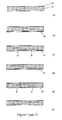
- the switch shown in Figures 1 and 2 comprises a rigid rectangular frame 1 supporting a first array of two optical fibres 2, 2' on one of its shorter edges and a second array of two optical fibres 3, 3' on one of its longer edges.
- collimators which may be of any known kind(s): thus they may be formed by one or more lenses aligned with the end of the fibre they serve; preformed lenses spliced by fusion or an adhesive to the end of the fibre (with or without additional aligned lenses); or lenses formed by fusing the end of the fibre, or a transparent extension to the fibre end, and shaping it by surface tension or by moulding (again with or without additional aligned lenses). It is particularly preferred to use one linear-bar collimator for each array to which all the fibres of the array are fusion pigtailed, so that alignment of the collimator to the switch is simplified.
- Each optical fibre defines an optical axis, represented in heavy dashed lines, and at each of the four places where a pair of these axes intersect, a platform 4, attached to but moveable with respect to the base-plate 1 in a manner to be described, supports a mirror 5, 5', 5a, 5a', inclined at 45° to both the axes and intersecting them when in the operative position in which they are drawn. They may, however, in accordance with the invention, be selectively moved by rectilinear translation, downwards as drawn, to inoperative positions in which they are below the top surface of the base-plate.
- FIG. 2 is a diagrammatic vertical section containing the optical axis of collimator 2, showing mirror 5 in its inoperative position and mirror 5' in its operative position.
- Each of the platforms 4 is connected to the frame 1 by tendons 6 at about the level of the top of the frame and tendons 7 at about the level of the bottom of the frame; as drawn in Figure 2 these are plain linear tendons monolithically connected to both the frame and the platform, but if (as is often likely to be the case) this does not permit sufficient movement, a more complex geometry may be used: by way of example, Figure 1 shows angular sinuous tendons 6.
- the tendons at the upper and lower levels are substantially identical in all respects (in particular, shape, dimensions and material, and therefore in elastic properties) and those in each layer are symmetrically arranged about the axis of their platform.
- the platforms are raised when required by actuators 8 which may be operated in any conventional manner: they are also lowered by them, unless the resilience of the tendons is sufficient to make it unnecessary.
- an abutment member 9 may be added to engage the mirror 5 when in its operative position, as an additional aid to ensuring that the platform 4 is not tilted when it is fully raised and that the mirror is correctly oriented.
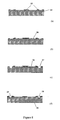
- Figure 3 shows an alternative approach to the design of the tendons (as seen, 6: tendons 7 are concealed below them and of identical structure). They take the form of a net of many intersecting members of relatively small cross-section. This is expected to reduce the risk that manufacturing variations will result in deleterious assymetry.
- Figure 4 illustrates one way in which the need for either stretching or substantial edgewise bending of any tendons is avoided: the platform 4 comprises a central block 10 (to support the mirror) mounted in a two-part rigid subframe 11, and the subframe is connected in accordance with the invention by tendons 6 and 7 (not visible) to the frame 1 and by auxiliary tendons 12 to the central block.
- the actuator 8 is shaped to act only on the subframe 11 and so the auxiliary tendons 12 are subjected to no substantial forces except the tension arising from the slight separation of the halves of the subframe as it rises: they may (among other possibilities) be in upper and lower layers like the tendons 6 and 7 or may extend the whole depth of the frame.
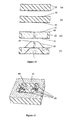
- Figure 5 outlines a first technique for the manufacture of one module of a freespace optical switch in accordance with the invention.
- the figure shows diagrammatic sections on the (111) plane of two ⁇ 110> oriented silicon wafers 13 and 14.
- the upper face of the first wafer 13 is appropriately prepared (one way of doing so will be described later) for the formation of a mirror at 15 and grooves for optical fibres (and preferably for collimator lenses) at 16; the lower faces of both wafers 13 and 14 are formed with respective tendons 6 and 7 (stage (a)).
- stage (b) the two wafers are bonded together.
- the wafers are wet etched along one of the (111) planes to fully form the mirror 5 and selectively etched away so that the platform 4 is connected to the surrounding frame 1 only by the tendons 6 and 7.
- Figure 6 shows a variant of this process which differs only in that the tendons 6 are formed in the upper face of the lower wafer 14 instead of the lower face of the upper wafer 13.
- the tendons (6 and 7) may be formed by any appropriate selective coating (printing) process, or by overall coating followed by pattern etching, according to techniques known in the semiconductor and micromechanical machining arts.
- Figure 7 illustrates successive steps in one practical implementation of the fabrication technique that was outlined in figure 5.
- One side of wafer 13 (1mm thick) is first masked by coating all over with silicon nitride (step (a)) and on the other side patterned with a diffusion mask 16 corresponding to the desired tendon structure (step (b)).
- Boron, and optionally germanium is diffused into the exposed silicon area (the area of the tendons 6) in a furnace, respectively to obtain etch resistance and stress control (step (c)).
- step (d) The patterned diffusion mask 16 is now removed and the surface coated all over with a silicon nitride etching mask 17 (step (d)) which is patterned to expose areas of silicon adjacent to the boron-diffused areas - by aligning the pattern with the underlying crystal structure of the silicon, anisotropic etching with potassium hydroxide can be used to etch substantially vertically into the wafer; selective wet-etching then allows the tendons 7 to be under-etched and thus freed from the substrate (step(e)), after which the mask 17 is removed (step (f)).
- a second wafer 14, 200 ⁇ m thick is processed on one side (its underside) in exactly the same way (steps (g) to (k)) and the two wafers are accurately aligned and bonded together (step (1)); known techniques of anodic bonding or of bonding by heat-treatment in the presence of water can be used.
- the silicon nitride etching mask 15 on the top face of the upper of the bonded wafers is now patterned in alignment with the crystal planes leaving an island 18 that will eventually define the position of the mirror (step (m)), and a fresh etching mask 19 applied to the top surface overall (step (n)); this mask may (among other available etching mask materials) be a photoresist or silicon nitride and is patterned (step (p)) to define whatever grooves and/or pits 20 are needed for locating and aligning optical fibres and/or lenses, and these are then developed by wet or dry etching (step (q)).
- This patterned mask 19 is now removed, leaving island 18 in place by virtue of its different material and/or greater thickness (step (r)) and a new overall silicon nitride or photoresist coating 21 for wet etching applied (step(s)).
- This is patterned in alignment with the crystal planes (step (t)) and the product is now ready for final etching. This is done by wet etching with potassium hydroxide at least in the region of the mirror 5, where its selective etching to the (111) crystal plane is needed, and the region of the tendons, where the resistance to etching of boron-diffused silicon is relied on.
- RIE reactive ion etching
- ICP inductive coupled plasma
- mirror 5 is suitably metallised - for 1550 nm telecommunication wavelengths, suitably with either gold or aluminium and, normally after separating multiple items by dicing or by fracturing along pre-etched boundary lines, fibre collimators represented by fibres 22 and spherical lenses 23 are bonded into their prepared positions.
- Figures 8-10 illustrate an alternative manufacturing technique, among other changes following the outline of Figure 6.
- Figure 8 shows steps in the preparation of a first wafer 24, which is first coated with silicon nitride 25 and patterned to define positions of the mirror and slots and/or pits for fibres and optional lenses (step (a)).
- the mirror area is protected with a photoresist 26 (step (b)) and the grooves and/or pits 27 dry etched with RIE or ICP (or if preferred could be wet etched) (step (c)).
- the photoresist 26 is removed and silicon nitride (or other coating resistant to potassium hydroxide) 28 applied and patterned to protect the grooves and/or pits (step (d)).
- a second wafer 29 is prepared as shown in Figure 9.
- a resist 30 is applied and patterned on both sides and shallow recesses 31 are dry or wet etched (steps (a) and (b)).
- the resist 30 is removed and silicon nitride 32 coated overall on both sides (step (c)); this is patterned in the base of each recess to define tendons, a requirement of this technique being that the tendons are not aligned with underlying crystal planes but the outlines around them are (step (d)).
- Photoresist 33 is applied to one face only, shown as the upper face, and patterned to protect the bases of the recesses on that face (step (e)) to allow the silicon nitride 32 to be removed from that face of the wafer while remaining in place in the recesses.
- the so-exposed face 33 of this wafer 29 is next bonded to the plain underface 34 of the first wafer 24 ( Figure 10, step (a)) and the assembly wet etched with potassium hydroxide from both sides; in this etching, the edges that are aligned with crystal planes are anisotropically etched to produce faces substantially perpendicular to the major faces of the wafers, but the edges of the tendons 6 and 7, not being so aligned, are undercut to free them from the substrate. Otherwise, the wafers are etched right through to free the platform 4 (steps (b) and (c)); metalising of the mirror 5, dicing and addition of collimator lenses 34 and optical fibres 35 completes the switch (step (d)).
- FIGS 11 and 12 illustrate an alternative manufacturing process which can be described quite briefly, since many of its steps are the same as for the process described and/or are known per se.
- this process only one chip is used in order to avoid the need for bonding chips together, and is processed identically on its two major faces. It is coated with photoresist 38 (stage (a)) which is patterned and developed to expose the chip surface through apertures 39 where the tendons are required (stage (b)); ion implantation is then used to introduce boron and/or germanium into the exposed parts of the chip surfaces.
- the photoresist is then removed, and a silicon nitride layer 40 applied and patterned to expose areas 41 whose edges are generally aligned with the crystal structure and which define the parts of the chip between the frame 42 and the implanted area, plus the edges of the implanted area.
- the chip is now etched with KOH (stage (c)), and since the implanted areas are relatively resistant to etching, enough of them remains to form tendons 43, which are seen at stage (d) with the platform 44 in its actuated position and in Figure 12 in its inactive position.
- a modification of this process provides for the use of metallic tendons.
- Silicon nitride is first applied and patterned to leave a protective coating over the area of the frame, and optionally the area of the tendons.
- a thin "seed layer" of gold is applied overall (preferably over one or more very thin layers selected to promote adhesion, e.g. a chromium layer), and then a thick photoresist layer is applied and patterned to form holes (exposing the gold surface) where the tendons are to be formed. More gold is applied by electroplating until the holes in the photoresist are nearly filled. The photoresist is removed and the part of the gold seed layer exposed by its removal etched away, leaving only the tendons as metallic parts. Since the gold is inherently resistant to KOH (other metals, if used as alternatives, may require protection), it is easy to under-etch the tendons and remove the unwanted material between them and the frame.
- Figures 13-16 illustrate some of the many tendon geometries that are suitable for use in applying the invention.
- tendons in the lower layer have been drawn as if they were smaller in cross section than those in the upper layer; in practice equal cross-sections will normally be preferred.
- the platform 4 that supports the mirror 5 is mounted from a surrounding rigid frame (not shown) by three tendons 6 which are coplanar and distributed uniformly (that is at 120° to each other) in the upper layer and three tendons 7 similarly distributed in the lower layer and each lying under one of those in the upper layer.
- Figure 14 is similar, except that the tendons 7 in the lower layer are each located midway between two of those in the upper layer (at 60° to each of them).
- the geometry of Figure 14 is thought to give the best control obtainable with only three tendons in each layer, and that of Figure 13 is considered rather easier to fabricate. These geometries are best suited to hexagonal, rather than rectangular, switch arrays.
- Figures 15 and 16 are similar to Figures 13 and 14 respectively, except that they have four tendons in each layer. They are likely to be preferred for rectangular switch arrays.
- the orientation of the tendons relative to the mirror can be optimized to minimize rotation on a chosen axis (notably the axis perpendicular to the light paths) at the cost of having more rotation around one or more axes (notably the axis perpendicular to the mirror surface) less important for the optical function of the mirror.
- Computer modeling could be used to chose the best configuration.
- the required fibres should be aligned by means of grooves in a suitable substrate chip formed with channels in the area of the beam intersections that can be filled with an index-matching liquid.
- the channels would be formed in the top face of the chip, and one of the mirror-support structures already described applied the opposite way up to the drawings, so that in their actuated positions the mirrors dip into the liquid.
Landscapes
- Physics & Mathematics (AREA)
- General Physics & Mathematics (AREA)
- Optics & Photonics (AREA)
- Electromagnetism (AREA)
- Mechanical Light Control Or Optical Switches (AREA)
Priority Applications (1)
| Application Number | Priority Date | Filing Date | Title |
|---|---|---|---|
| EP02290291A EP1335232A1 (fr) | 2002-02-07 | 2002-02-07 | Commutateurs optiques et leur méthode de fabrication |
Applications Claiming Priority (1)
| Application Number | Priority Date | Filing Date | Title |
|---|---|---|---|
| EP02290291A EP1335232A1 (fr) | 2002-02-07 | 2002-02-07 | Commutateurs optiques et leur méthode de fabrication |
Publications (1)
| Publication Number | Publication Date |
|---|---|
| EP1335232A1 true EP1335232A1 (fr) | 2003-08-13 |
Family
ID=27589176
Family Applications (1)
| Application Number | Title | Priority Date | Filing Date |
|---|---|---|---|
| EP02290291A Withdrawn EP1335232A1 (fr) | 2002-02-07 | 2002-02-07 | Commutateurs optiques et leur méthode de fabrication |
Country Status (1)
| Country | Link |
|---|---|
| EP (1) | EP1335232A1 (fr) |
Citations (6)
| Publication number | Priority date | Publication date | Assignee | Title |
|---|---|---|---|---|
| EP0286337A1 (fr) * | 1987-04-02 | 1988-10-12 | BRITISH TELECOMMUNICATIONS public limited company | Appareil de déflexion de radiation |
| US5396797A (en) * | 1991-02-08 | 1995-03-14 | Alliedsignal Inc. | Triaxial angular rate and acceleration sensor |
| DE29613520U1 (de) * | 1996-08-05 | 1996-09-19 | Forschungszentrum Karlsruhe GmbH, 76133 Karlsruhe | Mikrooptischer Schalter |
| US5594820A (en) * | 1995-02-08 | 1997-01-14 | Jds Fitel Inc. | Opto-mechanical device having optical element movable by twin flexures |
| US5742440A (en) * | 1995-10-25 | 1998-04-21 | Eastman Kodak Company | Actuator with reduced lens tilt error |
| EP1143283A2 (fr) * | 2000-04-05 | 2001-10-10 | Cronos Integrated Microsystems, Inc. | Commutateurs optiques micro-électromécaniques pour connexions croisées avec actionneurs mécaniques et méthodes d'opération |
-
2002
- 2002-02-07 EP EP02290291A patent/EP1335232A1/fr not_active Withdrawn
Patent Citations (6)
| Publication number | Priority date | Publication date | Assignee | Title |
|---|---|---|---|---|
| EP0286337A1 (fr) * | 1987-04-02 | 1988-10-12 | BRITISH TELECOMMUNICATIONS public limited company | Appareil de déflexion de radiation |
| US5396797A (en) * | 1991-02-08 | 1995-03-14 | Alliedsignal Inc. | Triaxial angular rate and acceleration sensor |
| US5594820A (en) * | 1995-02-08 | 1997-01-14 | Jds Fitel Inc. | Opto-mechanical device having optical element movable by twin flexures |
| US5742440A (en) * | 1995-10-25 | 1998-04-21 | Eastman Kodak Company | Actuator with reduced lens tilt error |
| DE29613520U1 (de) * | 1996-08-05 | 1996-09-19 | Forschungszentrum Karlsruhe GmbH, 76133 Karlsruhe | Mikrooptischer Schalter |
| EP1143283A2 (fr) * | 2000-04-05 | 2001-10-10 | Cronos Integrated Microsystems, Inc. | Commutateurs optiques micro-électromécaniques pour connexions croisées avec actionneurs mécaniques et méthodes d'opération |
Non-Patent Citations (1)
| Title |
|---|
| HOFFMANN M ET AL: "Bistable micromechanical fiber-optic switches on silicon with thermal actuators", SENSORS AND ACTUATORS A, ELSEVIER SEQUOIA S.A., LAUSANNE, CH, vol. 78, no. 1, January 1999 (1999-01-01), pages 28 - 35, XP004244577, ISSN: 0924-4247 * |
Similar Documents
| Publication | Publication Date | Title |
|---|---|---|
| US6541831B2 (en) | Single crystal silicon micromirror and array | |
| US6747784B2 (en) | Compliant mechanism and method of forming same | |
| DE60200251T2 (de) | Optischer Scanner und Herstellungsverfahren dafür | |
| US6941036B2 (en) | Microstructure relay switches | |
| EP1411024B1 (fr) | Actionneur bidimensionnel et son procédé de fabrication | |
| US6533947B2 (en) | Microelectromechanical mirror and mirror array | |
| US6449406B1 (en) | Micromachined optomechanical switching devices | |
| US6587626B2 (en) | Liquid overclad-encapsulated optical device | |
| US6411754B1 (en) | Micromechanical optical switch and method of manufacture | |
| US20050002084A1 (en) | Micro-electro-mechanical systems torsional drive | |
| DE60116839T2 (de) | Verfahren zur Herstellung einer Spiegelstruktur | |
| US6667823B2 (en) | Monolithic in-plane shutter switch | |
| KR100431581B1 (ko) | 미소거울 구동기 | |
| US20020164111A1 (en) | MEMS assemblies having moving members and methods of manufacturing the same | |
| EP1353205B1 (fr) | Alignement d'un assemblage de fibres utilisant des repères d'ajustage | |
| EP1335232A1 (fr) | Commutateurs optiques et leur méthode de fabrication | |
| US20040022482A1 (en) | Mem device | |
| US6980339B2 (en) | Deformable MEMS mirror | |
| Yee et al. | Fabrication and characterization of a PZT actuated micromirror with two-axis rotational motion for free space optics | |
| KR20040103977A (ko) | 마이크로 압전 액추에이터 및 그 제조 방법 | |
| US6773942B2 (en) | Method for making optical switch array | |
| US20020171909A1 (en) | Mems reflectors having tail portions that extend inside a recess and head portions that extend outside the recess and methods of forming same | |
| US20040095659A1 (en) | Micromirror actuator and method of manufacturing the same | |
| WO2001094253A2 (fr) | Structures massives de silicium a elements souples de film mince | |
| US7016128B2 (en) | Method of making a high reflectivity micro mirror and a micro mirror |
Legal Events
| Date | Code | Title | Description |
|---|---|---|---|
| PUAI | Public reference made under article 153(3) epc to a published international application that has entered the european phase |
Free format text: ORIGINAL CODE: 0009012 |
|
| AK | Designated contracting states |
Designated state(s): AT BE CH CY DE DK ES FI FR GB GR IE IT LI LU MC NL PT SE TR |
|
| AX | Request for extension of the european patent |
Extension state: AL LT LV MK RO SI |
|
| AKX | Designation fees paid | ||
| REG | Reference to a national code |
Ref country code: DE Ref legal event code: 8566 |
|
| STAA | Information on the status of an ep patent application or granted ep patent |
Free format text: STATUS: THE APPLICATION IS DEEMED TO BE WITHDRAWN |
|
| 18D | Application deemed to be withdrawn |
Effective date: 20040214 |