EP1335382A1 - Magnetisches Joch in MRAM zur Reduzierung des Programmierungsleistungsverbrauchs und Herstellungsverfahren - Google Patents
Magnetisches Joch in MRAM zur Reduzierung des Programmierungsleistungsverbrauchs und Herstellungsverfahren Download PDFInfo
- Publication number
- EP1335382A1 EP1335382A1 EP03250581A EP03250581A EP1335382A1 EP 1335382 A1 EP1335382 A1 EP 1335382A1 EP 03250581 A EP03250581 A EP 03250581A EP 03250581 A EP03250581 A EP 03250581A EP 1335382 A1 EP1335382 A1 EP 1335382A1
- Authority
- EP
- European Patent Office
- Prior art keywords
- layer
- fabricating
- substrate
- magnetic
- conductive line
- Prior art date
- Legal status (The legal status is an assumption and is not a legal conclusion. Google has not performed a legal analysis and makes no representation as to the accuracy of the status listed.)
- Granted
Links
Images





Classifications
-
- B—PERFORMING OPERATIONS; TRANSPORTING
- B82—NANOTECHNOLOGY
- B82Y—SPECIFIC USES OR APPLICATIONS OF NANOSTRUCTURES; MEASUREMENT OR ANALYSIS OF NANOSTRUCTURES; MANUFACTURE OR TREATMENT OF NANOSTRUCTURES
- B82Y10/00—Nanotechnology for information processing, storage or transmission, e.g. quantum computing or single electron logic
-
- G—PHYSICS
- G11—INFORMATION STORAGE
- G11C—STATIC STORES
- G11C11/00—Digital stores characterised by the use of particular electric or magnetic storage elements; Storage elements therefor
- G11C11/02—Digital stores characterised by the use of particular electric or magnetic storage elements; Storage elements therefor using magnetic elements
- G11C11/14—Digital stores characterised by the use of particular electric or magnetic storage elements; Storage elements therefor using magnetic elements using thin-film elements
- G11C11/15—Digital stores characterised by the use of particular electric or magnetic storage elements; Storage elements therefor using magnetic elements using thin-film elements using multiple magnetic layers
-
- G—PHYSICS
- G11—INFORMATION STORAGE
- G11C—STATIC STORES
- G11C11/00—Digital stores characterised by the use of particular electric or magnetic storage elements; Storage elements therefor
- G11C11/02—Digital stores characterised by the use of particular electric or magnetic storage elements; Storage elements therefor using magnetic elements
- G11C11/16—Digital stores characterised by the use of particular electric or magnetic storage elements; Storage elements therefor using magnetic elements using elements in which the storage effect is based on magnetic spin effect
- G11C11/161—Digital stores characterised by the use of particular electric or magnetic storage elements; Storage elements therefor using magnetic elements using elements in which the storage effect is based on magnetic spin effect details concerning the memory cell structure, e.g. the layers of the ferromagnetic memory cell
-
- G—PHYSICS
- G11—INFORMATION STORAGE
- G11C—STATIC STORES
- G11C11/00—Digital stores characterised by the use of particular electric or magnetic storage elements; Storage elements therefor
- G11C11/02—Digital stores characterised by the use of particular electric or magnetic storage elements; Storage elements therefor using magnetic elements
- G11C11/16—Digital stores characterised by the use of particular electric or magnetic storage elements; Storage elements therefor using magnetic elements using elements in which the storage effect is based on magnetic spin effect
- G11C11/165—Auxiliary circuits
- G11C11/1653—Address circuits or decoders
- G11C11/1655—Bit-line or column circuits
-
- G—PHYSICS
- G11—INFORMATION STORAGE
- G11C—STATIC STORES
- G11C11/00—Digital stores characterised by the use of particular electric or magnetic storage elements; Storage elements therefor
- G11C11/02—Digital stores characterised by the use of particular electric or magnetic storage elements; Storage elements therefor using magnetic elements
- G11C11/16—Digital stores characterised by the use of particular electric or magnetic storage elements; Storage elements therefor using magnetic elements using elements in which the storage effect is based on magnetic spin effect
- G11C11/165—Auxiliary circuits
- G11C11/1653—Address circuits or decoders
- G11C11/1657—Word-line or row circuits
-
- G—PHYSICS
- G11—INFORMATION STORAGE
- G11C—STATIC STORES
- G11C11/00—Digital stores characterised by the use of particular electric or magnetic storage elements; Storage elements therefor
- G11C11/02—Digital stores characterised by the use of particular electric or magnetic storage elements; Storage elements therefor using magnetic elements
- G11C11/16—Digital stores characterised by the use of particular electric or magnetic storage elements; Storage elements therefor using magnetic elements using elements in which the storage effect is based on magnetic spin effect
- G11C11/165—Auxiliary circuits
- G11C11/1675—Writing or programming circuits or methods
-
- H—ELECTRICITY
- H10—SEMICONDUCTOR DEVICES; ELECTRIC SOLID-STATE DEVICES NOT OTHERWISE PROVIDED FOR
- H10B—ELECTRONIC MEMORY DEVICES
- H10B61/00—Magnetic memory devices, e.g. magnetoresistive RAM [MRAM] devices
Definitions
- This invention relates to advanced non-volatile magnetic RAM (MRAM) devices, and specifically to a magnetic tunneling junction (MTJ) yoke structure for use in a MRAM device.
- MRAM magnetic RAM
- MTJ magnetic tunneling junction
- Magnetic RAM has an advantage over convention RAM because of its non-volatility and fast data access.
- magnetic tunneling junction MRAM appears to be the first type of MRAM device to reach production.
- Motorola aims to sample 4-Mbit MRAM in 2003, eetimes, February 2001.
- a MTJ includes two ferromagnetic layers which are separated by an insulating tunnel barrier layer.
- the magnetoresistance (MR) effect is the result of spin-polarization tunneling of conductive electrons between the two ferromagnetic layers.
- the tunneling current is a factor of the relative orientation of magnetic moments in the two ferromagnetic layers.
- MR magnetoresistance
- the large power requirement is the result of the writing process, in which a programming current in the milli-ampere range is required in order to switch a free magnetic layer in the MRAM.
- Data writing in MRAM devices is the result of the application of a magnetic field to a magnetic material, thereby magnetizing the material to one of two memory states. Reading is done by sensing a resistance charge in the magnetized material when a magnetic field is applied. Magnetic fields are created by a current passing through a line external to the magnetic material. as by passing a current through the magnetic material.
- An MRAM device includes a substrate; plural conductive lines, including a bit line and a word line; and a MTJ stack including a pair of magnetic yoke structures, wherein each of said yoke structures surrounds a conductive line.
- a method of fabricating a magnetic yoke structure in an MRAM structure includes preparing a substrate; forming a first conductive line on the substrate; fabricating a MTJ stack, including fabricating a first magnetic yoke structure about the first conductive line; forming a second conductive line on the MTJ stack; fabricating a second magnetic yoke suucture about the second conductive line; depositing a layer of oxide on the structure obtained by above steps; and metallizing the structure.
- Another object ofthe invention is to provide a magnetic yoke structure for use in an MRAM.
- a magnetic yoke structure is used in the device of the invention, and a method to make the magnetic yoke structure is described.
- the programming current is then reduced by 1/ ⁇ r, where ⁇ r is the magnetic permeability of the yoke. If the yoke material used is plated or sputtered NiFe, which has a ⁇ r of about 1000, a reduction of programming current to the ⁇ A range is achieved.
- a basic magnetic tunneling junction MRAM element is composed of the following layers: an anti-ferromagnetic (AF) layer, a ferromagnetic (FM) pinned layer, an insulating tunneling gap layer, and a ferromagnetic free layer, which are formed into a magnetoresistance stack. Additionally, bottom and top conducting wires are provided to facilitate read and write functions.
- AF anti-ferromagnetic
- FM ferromagnetic
- insulating tunneling gap layer an insulating tunneling gap layer
- ferromagnetic free layer which are formed into a magnetoresistance stack. Additionally, bottom and top conducting wires are provided to facilitate read and write functions.
- Fig. 1 illustrates a MRAM element 10, and a sandwich structure of a magnetic tunneling junction (MTJ) 12, and the related sensing circuitry, which are located on a substrate 14.
- substrate includes a silicon substrate and any layers of conducting, semi-conducting and insulating material fabricated on a silicon substrate. Additionally, the substrate may have MOS transistors fabricated thereon as part of the substrate preparation.
- the general structure of Fig. 1 includes conducting lines, such as a bit line 16, encapsulated in a horse shoe shaped magnetic yoke structure 18, and a word line 20, also encapsulated in a horse shoe shaped magnetic yoke structure 22, and a via 24, connected to a MOS transistor 26.
- MTJ 12 includes an AF pinned layer 28, an FM pinned layer 30, an insulating gap layer 32, a tunnel barrier layer 34, FM free layers 36, 38, and a bottom electrode 40.
- a seed layer and a capping layer are described later herein.
- Table 1 enumerates a set of parameters for each layer.
- Word line (WL) 20 is surrounded by soft magnetic material of magnetic yoke structure 42, which has a magnetic permeability of about 1000. Calculations indicates that, with the surrounding yoke structure, the programming current may be reduced to the ⁇ A range, and generates a 20 Oe programming field in the magnetic free layer, assuming layer thicknesses as given in Table 1. The programming current is about 4 mA, for the same structure, if no magnetic yoke structure is present.
- a silicon substrate 14 may be either n-type or p-type silicon.
- a layer of silicon dioxide 42 is deposited onto substrate 14 to a thickness of between about 500 nm to 1000 nm.
- Oxide layer 42 is etched to form a trench, having a depth of between about 400 nm to 900 nm, depending on the oxide layer thickness, but leaving about 100 nm of oxide on the substrate.
- a layer 44 of NiFe is deposited by sputtering to a thickness of about 200 nm.
- Another layer of silicon dioxide 46 is deposited by CVD, followed by deposition of a copper barrier layer 48, which may be TiN or WN, and a conductive line of copper 20 is deposited on copper barrier layer 48.
- the structure is smoothed by CMP to remove excess copper and to etch copper barrier layer 48.
- the structure is patterned and partially covered with photoresist to cover conductive line 20.
- the NiFe layer is removed by an ion milling etching process.
- the exposed surfaces are covered with silicon dioxide layer 50, after which the structure is smoothed by CMP to expose the conductive line.
- a MTJ stack 12 is then formed on conductive line 20.
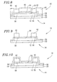
- Figs 4-13 depicts successive steps in the fabrication of a magnetic yoke structure for use in an MRAM according to the invention in greater detail.
- Fig. 4 depicts silicon substrate 14, which may have one or more MOS transistors formed thereon.
- Word line (WL) 20 is formed as previously described and encapsulated in first magnetic yoke structure 22.
- WL referred to herein as a first conductive line, may be formed of a suitable metal, such as aluminum, copper, or platinum, although copper is preferred, to a thickness of between about 400 nm to 900 nm.
- MTJ stack 12 is fabricated on WL 20 in this embodiment of the invention, and contains the layers of materials listed in Table 1, deposited to the thicknesses listed in Table 1.
- the WL and MTJ stack are covered by a layer of oxide 56. deposited by CVD to a thickness of between about 50 nm to 100 nm.
- the oxide layer is patterned and etched to expose portions of the MTJ stack.
- a layer of NiFe 58 is deposited over the structure to a thickness of about 100 nm. This layer provides a seed layer for subsequent yoke plating.
- photoresist 60 is applied and another layer of NiFe 62 is deposited providing for a total NiFe thickness of about 1000 nm.
- the photoresist is stripped and the NiFe is ion milled to remove the NiFe overlaying the oxide, leaving the thicker NiFe layer over those portions of the structure which had the oxide previously removed.
- a layer of oxide 64 is deposited by CVD to a thickness of between about 50 nm to 100 nm, completely covering the structure.
- bit line (BL) 16 referred to herein as a second conductive line.
- CMP chemical mechanical polishing
- a layer of oxide 70 is deposited over the structure to a thickness of about 100 nm. The oxide is masked and etched, to open the top of the NiFe layer magnetic contact. Another layer of NiFe 72 is deposited to a thickness of about 200 nm. NiFe elements 62 and 72 form an encapsulating structure 18 for BL 16, which has a horse shoe configuration, as does encapsulating structure 22.
- the structure is patterned, and the NiFe is removed by ion milling on the left side of the figure.
- the NiFe material on the right side of the figure is connecter to transistor 26.
- the structure is completed and finished by appropriate metallization.
- the BL and WL may be interchanged, i.e ., the BL may be formed as the second conductive line and the WL may be formed as the first conductive line, therefore, the fabrication process for these structures and their magnetic yoke structures may also be interchanged.
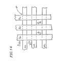
- FIG. 14 An alternate method of fabricate an MRAM according to the method of the invention is described in conjunction with Figs. 14-21.
- Fig. 14 the structure is depicted in a top plan view, showing the orientation of the remaining Figs 15-21.
- the left side of the figure is a cross-section taken parallel to the BL, view A-A, while the right side of the figure is a cross-section taken parallel to the WL, view B-B.
- the first step in fabricating a magnetic yoke structure 80 according to the invention is preparing a substrate 82.
- the substrate may be a silicon wafer of either n-type or p-type, with MOS transistors fabricated thereon. As shown in Fig.
- an oxide layer 84 is formed on the substrate to a thickness of between about 500 nm to 1000 nm.
- the oxide layer 84 is patterned and etched by a dual damascene process, and metal for a WL 86 is deposited, as by CVD or PVD.
- the metal deposited may be aluminum, copper or platinum.
- a fixed magnetic layer stack 88 of Ta, NiMn, CoFe; Ta, FeMn, CoFe: or Ta, NiFe, FeMn, CoFe is deposited to a thickness of between about 45 nm to 55 nm and a layer 90 of Al x O y is deposited to a thickness of between about one nm to two nm to form a tunnel barrier layer.
- a free magnetic layer 92 of NiFe is then deposited to a thickness of between about seven nm to twelve nm, followed by a layer of silicon nitride 94, which is deposited to a thickness of between about 500 nm to 1000 nm.
- the structure is patterned and etched, resulting in the memory stack structure of Fig. 15.
- a layer of oxide 96 is deposited to a thickness of between about 800 nm and 1400 nm.
- the structure is smoothed by CMP, resulting in the structure of Fig. 16.
- the structure is covered with photoresist and appropriate vias and trenches are formed to a depth of between about 500 nm and 1000 nm, by a dual damascene process to form BL trenches 98.
- Oxide layer 96 is then etched, as is silicon nitride layer 94, resulting in the structure of Fig. 17.
- Fig. 18 copper is deposited by CVD into the BL trenches, forming BL 100, and finished by CMP. Silicon nitride layer 94 is removed by a wet etch process, resulting in the structure of Fig. 19.
- a second free magnetic layer 102 is deposited to a thickness of between about 500 nm to 1000 nm, overlying the BL, and filling the trenches left by the nitride removal. Portions of the second free magnetic layer are covered with photoresist, and the remainder is removed by etching, leaving the structure of Fig. 20.
- a layer of oxide 104 is deposited to a thickness of between about 1000 nm and 2000 nm, passivated, and the structure metallized (not shown), completing the magnetic yoke structure of the invention.
- the structure may be inverted, i.e. , the BL may be on the bottom of the MR stack and the WL may be on the top of the stack.
Landscapes
- Engineering & Computer Science (AREA)
- Computer Hardware Design (AREA)
- Chemical & Material Sciences (AREA)
- Nanotechnology (AREA)
- Physics & Mathematics (AREA)
- Mathematical Physics (AREA)
- Theoretical Computer Science (AREA)
- Crystallography & Structural Chemistry (AREA)
- Mram Or Spin Memory Techniques (AREA)
- Hall/Mr Elements (AREA)
- Semiconductor Memories (AREA)
Applications Claiming Priority (2)
| Application Number | Priority Date | Filing Date | Title |
|---|---|---|---|
| US10/061,974 US6548849B1 (en) | 2002-01-31 | 2002-01-31 | Magnetic yoke structures in MRAM devices to reduce programming power consumption and a method to make the same |
| US61974 | 2002-01-31 |
Publications (2)
| Publication Number | Publication Date |
|---|---|
| EP1335382A1 true EP1335382A1 (de) | 2003-08-13 |
| EP1335382B1 EP1335382B1 (de) | 2006-09-27 |
Family
ID=22039401
Family Applications (1)
| Application Number | Title | Priority Date | Filing Date |
|---|---|---|---|
| EP03250581A Expired - Lifetime EP1335382B1 (de) | 2002-01-31 | 2003-01-30 | Magnetisches Joch in MRAM zur Reduzierung des Programmierungsleistungsverbrauchs und Herstellungsverfahren |
Country Status (7)
| Country | Link |
|---|---|
| US (2) | US6548849B1 (de) |
| EP (1) | EP1335382B1 (de) |
| JP (1) | JP2003243633A (de) |
| KR (1) | KR100544085B1 (de) |
| CN (1) | CN100345214C (de) |
| DE (1) | DE60308568T2 (de) |
| TW (1) | TWI282162B (de) |
Cited By (3)
| Publication number | Priority date | Publication date | Assignee | Title |
|---|---|---|---|---|
| EP1387400A3 (de) * | 2002-07-30 | 2008-04-23 | Kabushiki Kaisha Toshiba | Magnetische Speicheranordnung mit einer Rückschlussschicht und deren Herstellungsverfahren |
| DE102005035166B4 (de) * | 2004-08-20 | 2009-05-14 | Altis Semiconductor Snc | Magnetisches Speicherelement mit magnetischer Durchführung und magnetischem Sensorelement sowie magnetischem Direktzugriffsspeicher |
| DE102005034665B4 (de) * | 2004-07-26 | 2011-04-14 | International Business Machines Corp. | Verfahren zum Herstellen einer Leiterbahn einer resistiven Speichereinrichtung |
Families Citing this family (55)
| Publication number | Priority date | Publication date | Assignee | Title |
|---|---|---|---|---|
| DE10110292C1 (de) * | 2001-02-26 | 2002-10-02 | Dresden Ev Inst Festkoerper | Stromabhängiges resistives Bauelement |
| CN100350496C (zh) * | 2001-11-30 | 2007-11-21 | 株式会社东芝 | 磁存储装置及其制造方法 |
| JP4053825B2 (ja) * | 2002-01-22 | 2008-02-27 | 株式会社東芝 | 半導体集積回路装置 |
| US6548849B1 (en) * | 2002-01-31 | 2003-04-15 | Sharp Laboratories Of America, Inc. | Magnetic yoke structures in MRAM devices to reduce programming power consumption and a method to make the same |
| US6665205B2 (en) * | 2002-02-20 | 2003-12-16 | Hewlett-Packard Development Company, Lp. | Shared global word line magnetic random access memory |
| JP3993522B2 (ja) * | 2002-03-29 | 2007-10-17 | 株式会社東芝 | 磁気記憶装置の製造方法 |
| US6873023B2 (en) * | 2002-04-18 | 2005-03-29 | Kabushiki Kaisha Toshiba | Magnetic random access memory |
| JP3898556B2 (ja) * | 2002-04-22 | 2007-03-28 | 株式会社東芝 | 磁気ランダムアクセスメモリ |
| US6707083B1 (en) * | 2002-07-09 | 2004-03-16 | Western Digital (Fremont), Inc. | Magnetic tunneling junction with improved power consumption |
| US6680500B1 (en) * | 2002-07-31 | 2004-01-20 | Infineon Technologies Ag | Insulating cap layer and conductive cap layer for semiconductor devices with magnetic material layers |
| US6770491B2 (en) * | 2002-08-07 | 2004-08-03 | Micron Technology, Inc. | Magnetoresistive memory and method of manufacturing the same |
| US6914805B2 (en) * | 2002-08-21 | 2005-07-05 | Micron Technology, Inc. | Method for building a magnetic keeper or flux concentrator used for writing magnetic bits on a MRAM device |
| JP3906139B2 (ja) * | 2002-10-16 | 2007-04-18 | 株式会社東芝 | 磁気ランダムアクセスメモリ |
| JP3906145B2 (ja) * | 2002-11-22 | 2007-04-18 | 株式会社東芝 | 磁気ランダムアクセスメモリ |
| US6952364B2 (en) * | 2003-03-03 | 2005-10-04 | Samsung Electronics Co., Ltd. | Magnetic tunnel junction structures and methods of fabrication |
| KR100615600B1 (ko) * | 2004-08-09 | 2006-08-25 | 삼성전자주식회사 | 고집적 자기램 소자 및 그 제조방법 |
| JP2005044847A (ja) * | 2003-07-23 | 2005-02-17 | Tdk Corp | 磁気抵抗効果素子、磁気記憶セルおよび磁気メモリデバイスならびにそれらの製造方法 |
| US7078239B2 (en) * | 2003-09-05 | 2006-07-18 | Micron Technology, Inc. | Integrated circuit structure formed by damascene process |
| JP4247085B2 (ja) * | 2003-09-29 | 2009-04-02 | 株式会社東芝 | 磁気記憶装置およびその製造方法 |
| US6900491B2 (en) * | 2003-10-06 | 2005-05-31 | Hewlett-Packard Development Company, L.P. | Magnetic memory |
| US20050141148A1 (en) * | 2003-12-02 | 2005-06-30 | Kabushiki Kaisha Toshiba | Magnetic memory |
| US6969895B2 (en) * | 2003-12-10 | 2005-11-29 | Headway Technologies, Inc. | MRAM cell with flat topography and controlled bit line to free layer distance and method of manufacture |
| JP2005260082A (ja) * | 2004-03-12 | 2005-09-22 | Toshiba Corp | 磁気ランダムアクセスメモリ |
| JP2005260083A (ja) * | 2004-03-12 | 2005-09-22 | Toshiba Corp | 磁気ランダムアクセスメモリ |
| US7211446B2 (en) * | 2004-06-11 | 2007-05-01 | International Business Machines Corporation | Method of patterning a magnetic tunnel junction stack for a magneto-resistive random access memory |
| US7611912B2 (en) * | 2004-06-30 | 2009-11-03 | Headway Technologies, Inc. | Underlayer for high performance magnetic tunneling junction MRAM |
| US7321734B2 (en) * | 2004-07-29 | 2008-01-22 | Nortel Networks Limited | Digital synthesis of readily compensated optical signals |
| KR100660539B1 (ko) | 2004-07-29 | 2006-12-22 | 삼성전자주식회사 | 자기 기억 소자 및 그 형성 방법 |
| US7122386B1 (en) | 2005-09-21 | 2006-10-17 | Magic Technologies, Inc. | Method of fabricating contact pad for magnetic random access memory |
| JP4444257B2 (ja) | 2006-09-08 | 2010-03-31 | 株式会社東芝 | スピンfet |
| US7456029B2 (en) * | 2006-06-28 | 2008-11-25 | Magic Technologies, Inc. | Planar flux concentrator for MRAM devices |
| US20080232761A1 (en) * | 2006-09-20 | 2008-09-25 | Raveen Kumaran | Methods of making optical waveguide structures by way of molecular beam epitaxy |
| WO2008047240A2 (en) * | 2006-09-20 | 2008-04-24 | Zecotek Medical Systems Inc. | Methods of making optical waveguide structures by way of molecular beam epitaxy |
| US8542524B2 (en) * | 2007-02-12 | 2013-09-24 | Avalanche Technology, Inc. | Magnetic random access memory (MRAM) manufacturing process for a small magnetic tunnel junction (MTJ) design with a low programming current requirement |
| US7760542B2 (en) * | 2008-04-21 | 2010-07-20 | Seagate Technology Llc | Spin-torque memory with unidirectional write scheme |
| US7974119B2 (en) | 2008-07-10 | 2011-07-05 | Seagate Technology Llc | Transmission gate-based spin-transfer torque memory unit |
| US8233319B2 (en) | 2008-07-18 | 2012-07-31 | Seagate Technology Llc | Unipolar spin-transfer switching memory unit |
| US7933137B2 (en) * | 2008-10-08 | 2011-04-26 | Seagate Teachnology Llc | Magnetic random access memory (MRAM) utilizing magnetic flip-flop structures |
| US7933146B2 (en) * | 2008-10-08 | 2011-04-26 | Seagate Technology Llc | Electronic devices utilizing spin torque transfer to flip magnetic orientation |
| US20100091546A1 (en) * | 2008-10-15 | 2010-04-15 | Seagate Technology Llc | High density reconfigurable spin torque non-volatile memory |
| US9030867B2 (en) | 2008-10-20 | 2015-05-12 | Seagate Technology Llc | Bipolar CMOS select device for resistive sense memory |
| US7936580B2 (en) | 2008-10-20 | 2011-05-03 | Seagate Technology Llc | MRAM diode array and access method |
| US7936583B2 (en) | 2008-10-30 | 2011-05-03 | Seagate Technology Llc | Variable resistive memory punchthrough access method |
| US7825478B2 (en) | 2008-11-07 | 2010-11-02 | Seagate Technology Llc | Polarity dependent switch for resistive sense memory |
| US8178864B2 (en) | 2008-11-18 | 2012-05-15 | Seagate Technology Llc | Asymmetric barrier diode |
| US8203869B2 (en) | 2008-12-02 | 2012-06-19 | Seagate Technology Llc | Bit line charge accumulation sensing for resistive changing memory |
| US8159856B2 (en) | 2009-07-07 | 2012-04-17 | Seagate Technology Llc | Bipolar select device for resistive sense memory |
| US8158964B2 (en) | 2009-07-13 | 2012-04-17 | Seagate Technology Llc | Schottky diode switch and memory units containing the same |
| US8208290B2 (en) * | 2009-08-26 | 2012-06-26 | Qualcomm Incorporated | System and method to manufacture magnetic random access memory |
| US8648426B2 (en) | 2010-12-17 | 2014-02-11 | Seagate Technology Llc | Tunneling transistors |
| CN102938257B (zh) * | 2011-08-15 | 2017-05-17 | 中芯国际集成电路制造(上海)有限公司 | 磁隧道结、其制作方法及含磁隧道结的存储单元 |
| US9023699B2 (en) * | 2012-12-20 | 2015-05-05 | Taiwan Semiconductor Manufacturing Company, Ltd. | Resistive random access memory (RRAM) structure and method of making the RRAM structure |
| KR102465539B1 (ko) | 2015-09-18 | 2022-11-11 | 삼성전자주식회사 | 자기 터널 접합 구조체를 포함하는 반도체 소자 및 그의 형성 방법 |
| US11309216B2 (en) * | 2020-01-27 | 2022-04-19 | International Business Machines Corporation | Large grain copper interconnect lines for MRAM |
| WO2022016313A1 (zh) * | 2020-07-20 | 2022-01-27 | 中国科学院微电子研究所 | 缓存器件及制作方法 |
Citations (7)
| Publication number | Priority date | Publication date | Assignee | Title |
|---|---|---|---|---|
| US5640343A (en) * | 1996-03-18 | 1997-06-17 | International Business Machines Corporation | Magnetic memory array using magnetic tunnel junction devices in the memory cells |
| WO2000072324A1 (en) * | 1999-05-25 | 2000-11-30 | Honeywell Inc. | Local shielding for memory cells |
| US6211090B1 (en) * | 2000-03-21 | 2001-04-03 | Motorola, Inc. | Method of fabricating flux concentrating layer for use with magnetoresistive random access memories |
| EP1107329A2 (de) * | 1999-12-10 | 2001-06-13 | Sharp Kabushiki Kaisha | Magnetische Tunnelübergangsanordnung, magnetische Speicheranordnung, magnetische Speicherzelle und Zugriffsverfahren |
| WO2002084755A2 (en) * | 2001-02-28 | 2002-10-24 | Micron Technology, Inc. | Keepers for mram electrodes |
| WO2003019569A2 (en) * | 2001-08-27 | 2003-03-06 | Motorola Inc. | Magneto-electronic component |
| EP1296332A2 (de) * | 2001-09-25 | 2003-03-26 | Hewlett-Packard Company | Magnetischer Datenspeicher |
Family Cites Families (6)
| Publication number | Priority date | Publication date | Assignee | Title |
|---|---|---|---|---|
| US6183859B1 (en) | 1998-07-20 | 2001-02-06 | Motorola, Inc | Low resistance MTJ |
| US6034887A (en) * | 1998-08-05 | 2000-03-07 | International Business Machines Corporation | Non-volatile magnetic memory cell and devices |
| DE19836567C2 (de) * | 1998-08-12 | 2000-12-07 | Siemens Ag | Speicherzellenanordnung mit Speicherelementen mit magnetoresistivem Effekt und Verfahren zu deren Herstellung |
| JP2003505878A (ja) * | 1999-07-22 | 2003-02-12 | コーニンクレッカ フィリップス エレクトロニクス エヌ ヴィ | 磁気トンネル接合装置を製造する方法 |
| US6304477B1 (en) | 2001-01-31 | 2001-10-16 | Motorola, Inc. | Content addressable magnetic random access memory |
| US6548849B1 (en) * | 2002-01-31 | 2003-04-15 | Sharp Laboratories Of America, Inc. | Magnetic yoke structures in MRAM devices to reduce programming power consumption and a method to make the same |
-
2002
- 2002-01-31 US US10/061,974 patent/US6548849B1/en not_active Expired - Lifetime
-
2003
- 2003-01-21 JP JP2003012841A patent/JP2003243633A/ja active Pending
- 2003-01-30 EP EP03250581A patent/EP1335382B1/de not_active Expired - Lifetime
- 2003-01-30 CN CNB031034608A patent/CN100345214C/zh not_active Expired - Lifetime
- 2003-01-30 DE DE60308568T patent/DE60308568T2/de not_active Expired - Lifetime
- 2003-01-30 TW TW092102298A patent/TWI282162B/zh not_active IP Right Cessation
- 2003-01-30 KR KR1020030006139A patent/KR100544085B1/ko not_active Expired - Fee Related
- 2003-03-10 US US10/385,390 patent/US6709942B2/en not_active Expired - Lifetime
Patent Citations (7)
| Publication number | Priority date | Publication date | Assignee | Title |
|---|---|---|---|---|
| US5640343A (en) * | 1996-03-18 | 1997-06-17 | International Business Machines Corporation | Magnetic memory array using magnetic tunnel junction devices in the memory cells |
| WO2000072324A1 (en) * | 1999-05-25 | 2000-11-30 | Honeywell Inc. | Local shielding for memory cells |
| EP1107329A2 (de) * | 1999-12-10 | 2001-06-13 | Sharp Kabushiki Kaisha | Magnetische Tunnelübergangsanordnung, magnetische Speicheranordnung, magnetische Speicherzelle und Zugriffsverfahren |
| US6211090B1 (en) * | 2000-03-21 | 2001-04-03 | Motorola, Inc. | Method of fabricating flux concentrating layer for use with magnetoresistive random access memories |
| WO2002084755A2 (en) * | 2001-02-28 | 2002-10-24 | Micron Technology, Inc. | Keepers for mram electrodes |
| WO2003019569A2 (en) * | 2001-08-27 | 2003-03-06 | Motorola Inc. | Magneto-electronic component |
| EP1296332A2 (de) * | 2001-09-25 | 2003-03-26 | Hewlett-Packard Company | Magnetischer Datenspeicher |
Non-Patent Citations (2)
| Title |
|---|
| WANG Z G ET AL: "FEASIBILITY OF ULTRA-DENSE SPIN-TUNNELING RANDOM ACCESS MEMORY", IEEE TRANSACTIONS ON MAGNETICS, IEEE INC. NEW YORK, US, vol. 33, no. 6, November 1997 (1997-11-01), pages 4498 - 4512, XP000831059, ISSN: 0018-9464 * |
| Y.SAITO: "Current status and advanced future technology in order to realize high-density", FED, 2001, XP002240920, Retrieved from the Internet <URL:www.fed.or.jp/pub/review/FEDreviewV1N25E1SaitoY.pdfwww.fed.or.jp/pub/review/FEDreviewV1N25E1SaitoY.pdf> [retrieved on 20030512] * |
Cited By (4)
| Publication number | Priority date | Publication date | Assignee | Title |
|---|---|---|---|---|
| EP1387400A3 (de) * | 2002-07-30 | 2008-04-23 | Kabushiki Kaisha Toshiba | Magnetische Speicheranordnung mit einer Rückschlussschicht und deren Herstellungsverfahren |
| DE102005034665B4 (de) * | 2004-07-26 | 2011-04-14 | International Business Machines Corp. | Verfahren zum Herstellen einer Leiterbahn einer resistiven Speichereinrichtung |
| DE102005034665B9 (de) * | 2004-07-26 | 2012-09-06 | International Business Machines Corp. | Verfahren zum Herstellen einer Leiterbahn einer resistiven Speichereinrichtung |
| DE102005035166B4 (de) * | 2004-08-20 | 2009-05-14 | Altis Semiconductor Snc | Magnetisches Speicherelement mit magnetischer Durchführung und magnetischem Sensorelement sowie magnetischem Direktzugriffsspeicher |
Also Published As
| Publication number | Publication date |
|---|---|
| CN1435841A (zh) | 2003-08-13 |
| CN100345214C (zh) | 2007-10-24 |
| TW200400622A (en) | 2004-01-01 |
| US20030168684A1 (en) | 2003-09-11 |
| TWI282162B (en) | 2007-06-01 |
| JP2003243633A (ja) | 2003-08-29 |
| KR20030066393A (ko) | 2003-08-09 |
| KR100544085B1 (ko) | 2006-01-23 |
| DE60308568D1 (de) | 2006-11-09 |
| US6548849B1 (en) | 2003-04-15 |
| US6709942B2 (en) | 2004-03-23 |
| EP1335382B1 (de) | 2006-09-27 |
| DE60308568T2 (de) | 2007-05-31 |
Similar Documents
| Publication | Publication Date | Title |
|---|---|---|
| US6548849B1 (en) | Magnetic yoke structures in MRAM devices to reduce programming power consumption and a method to make the same | |
| US7919794B2 (en) | Memory cell and method of forming a magnetic tunnel junction (MTJ) of a memory cell | |
| TW519680B (en) | Self-aligned magnetic clad write line and its method of formation | |
| US6864551B2 (en) | High density and high programming efficiency MRAM design | |
| US6783994B2 (en) | Method of fabricating a self-aligned magnetic tunneling junction and via contact | |
| JP4583997B2 (ja) | 磁気メモリセルアレイおよびその製造方法 | |
| US7169622B2 (en) | Magnetoresistive random access memory devices and methods for fabricating the same | |
| US7205590B2 (en) | Semiconductor memory device provided with magneto-resistive element and method for fabricating the same | |
| US6982445B2 (en) | MRAM architecture with a bit line located underneath the magnetic tunneling junction device | |
| US6465262B2 (en) | Method for manufacturing a semiconductor device | |
| US7334317B2 (en) | Method of forming magnetoresistive junctions in manufacturing MRAM cells | |
| US6849466B2 (en) | Method for manufacturing MTJ cell of magnetic random access memory | |
| TW202545299A (zh) | 磁阻式隨機存取記憶體及其製作方法 | |
| CN1748323A (zh) | 高密度和高编程效率的mram设计 |
Legal Events
| Date | Code | Title | Description |
|---|---|---|---|
| PUAI | Public reference made under article 153(3) epc to a published international application that has entered the european phase |
Free format text: ORIGINAL CODE: 0009012 |
|
| AK | Designated contracting states |
Designated state(s): AT BE BG CH CY CZ DE DK EE ES FI FR GB GR HU IE IT LI LU MC NL PT SE SI SK TR |
|
| AX | Request for extension of the european patent |
Extension state: AL LT LV MK RO |
|
| 17P | Request for examination filed |
Effective date: 20040205 |
|
| AKX | Designation fees paid |
Designated state(s): DE GB |
|
| RBV | Designated contracting states (corrected) |
Designated state(s): DE FR GB |
|
| 17Q | First examination report despatched |
Effective date: 20050201 |
|
| GRAP | Despatch of communication of intention to grant a patent |
Free format text: ORIGINAL CODE: EPIDOSNIGR1 |
|
| GRAS | Grant fee paid |
Free format text: ORIGINAL CODE: EPIDOSNIGR3 |
|
| GRAA | (expected) grant |
Free format text: ORIGINAL CODE: 0009210 |
|
| AK | Designated contracting states |
Kind code of ref document: B1 Designated state(s): DE FR GB |
|
| REG | Reference to a national code |
Ref country code: GB Ref legal event code: FG4D |
|
| REF | Corresponds to: |
Ref document number: 60308568 Country of ref document: DE Date of ref document: 20061109 Kind code of ref document: P |
|
| ET | Fr: translation filed | ||
| PLBE | No opposition filed within time limit |
Free format text: ORIGINAL CODE: 0009261 |
|
| STAA | Information on the status of an ep patent application or granted ep patent |
Free format text: STATUS: NO OPPOSITION FILED WITHIN TIME LIMIT |
|
| 26N | No opposition filed |
Effective date: 20070628 |
|
| PGFP | Annual fee paid to national office [announced via postgrant information from national office to epo] |
Ref country code: GB Payment date: 20150121 Year of fee payment: 13 |
|
| REG | Reference to a national code |
Ref country code: FR Ref legal event code: PLFP Year of fee payment: 14 |
|
| GBPC | Gb: european patent ceased through non-payment of renewal fee |
Effective date: 20160130 |
|
| PG25 | Lapsed in a contracting state [announced via postgrant information from national office to epo] |
Ref country code: GB Free format text: LAPSE BECAUSE OF NON-PAYMENT OF DUE FEES Effective date: 20160130 |
|
| REG | Reference to a national code |
Ref country code: FR Ref legal event code: PLFP Year of fee payment: 15 |
|
| REG | Reference to a national code |
Ref country code: FR Ref legal event code: PLFP Year of fee payment: 16 |
|
| PGFP | Annual fee paid to national office [announced via postgrant information from national office to epo] |
Ref country code: DE Payment date: 20220119 Year of fee payment: 20 |
|
| PGFP | Annual fee paid to national office [announced via postgrant information from national office to epo] |
Ref country code: FR Payment date: 20220119 Year of fee payment: 20 |
|
| REG | Reference to a national code |
Ref country code: DE Ref legal event code: R071 Ref document number: 60308568 Country of ref document: DE |