EP1335452A2 - Dispostion de mise en contact de deux structures métaliques - Google Patents
Dispostion de mise en contact de deux structures métaliques Download PDFInfo
- Publication number
- EP1335452A2 EP1335452A2 EP03000900A EP03000900A EP1335452A2 EP 1335452 A2 EP1335452 A2 EP 1335452A2 EP 03000900 A EP03000900 A EP 03000900A EP 03000900 A EP03000900 A EP 03000900A EP 1335452 A2 EP1335452 A2 EP 1335452A2
- Authority
- EP
- European Patent Office
- Prior art keywords
- metal
- insulating layer
- metal structures
- metal structure
- structures
- Prior art date
- Legal status (The legal status is an assumption and is not a legal conclusion. Google has not performed a legal analysis and makes no representation as to the accuracy of the status listed.)
- Withdrawn
Links
Images

Classifications
-
- H—ELECTRICITY
- H05—ELECTRIC TECHNIQUES NOT OTHERWISE PROVIDED FOR
- H05K—PRINTED CIRCUITS; CASINGS OR CONSTRUCTIONAL DETAILS OF ELECTRIC APPARATUS; MANUFACTURE OF ASSEMBLAGES OF ELECTRICAL COMPONENTS
- H05K3/00—Apparatus or processes for manufacturing printed circuits
- H05K3/40—Forming printed elements for providing electric connections to or between printed circuits
- H05K3/4038—Through-connections; Vertical interconnect access [VIA] connections
- H05K3/4084—Through-connections; Vertical interconnect access [VIA] connections by deforming at least one of the conductive layers
-
- H—ELECTRICITY
- H05—ELECTRIC TECHNIQUES NOT OTHERWISE PROVIDED FOR
- H05K—PRINTED CIRCUITS; CASINGS OR CONSTRUCTIONAL DETAILS OF ELECTRIC APPARATUS; MANUFACTURE OF ASSEMBLAGES OF ELECTRICAL COMPONENTS
- H05K2203/00—Indexing scheme relating to apparatus or processes for manufacturing printed circuits covered by H05K3/00
- H05K2203/11—Treatments characterised by their effect, e.g. heating, cooling, roughening
- H05K2203/1189—Pressing leads, bumps or a die through an insulating layer
-
- H—ELECTRICITY
- H05—ELECTRIC TECHNIQUES NOT OTHERWISE PROVIDED FOR
- H05K—PRINTED CIRCUITS; CASINGS OR CONSTRUCTIONAL DETAILS OF ELECTRIC APPARATUS; MANUFACTURE OF ASSEMBLAGES OF ELECTRICAL COMPONENTS
- H05K2203/00—Indexing scheme relating to apparatus or processes for manufacturing printed circuits covered by H05K3/00
- H05K2203/15—Position of the PCB during processing
- H05K2203/1572—Processing both sides of a PCB by the same process; Providing a similar arrangement of components on both sides; Making interlayer connections from two sides
-
- H—ELECTRICITY
- H05—ELECTRIC TECHNIQUES NOT OTHERWISE PROVIDED FOR
- H05K—PRINTED CIRCUITS; CASINGS OR CONSTRUCTIONAL DETAILS OF ELECTRIC APPARATUS; MANUFACTURE OF ASSEMBLAGES OF ELECTRICAL COMPONENTS
- H05K3/00—Apparatus or processes for manufacturing printed circuits
- H05K3/10—Apparatus or processes for manufacturing printed circuits in which conductive material is applied to the insulating support in such a manner as to form the desired conductive pattern
- H05K3/20—Apparatus or processes for manufacturing printed circuits in which conductive material is applied to the insulating support in such a manner as to form the desired conductive pattern by affixing prefabricated conductor pattern
- H05K3/202—Apparatus or processes for manufacturing printed circuits in which conductive material is applied to the insulating support in such a manner as to form the desired conductive pattern by affixing prefabricated conductor pattern using self-supporting metal foil pattern
Definitions
- the invention relates to a method for contacting conductive layers of a metal-plastic laminate.
- DE 198 52 832 discloses a method for producing a metal-plastic laminate in which at least one metal foil is first attached to at least one plastic foil, for example glued, the metal foil by embossing and / or deep drawing at least one Shaped metal contact surface and then the metal foil while maintaining (almost) the Metal contact surface profile is laminated with at least one plastic film. Furthermore, described there, at least one metal foil by embossing and / or deep drawing at least to form a metal contact surface and the metal foil with at least one plastic foil to laminate that the metal contact surface profile of the metal foil is almost preserved, whereby the at least one metal contact surface after lamination has a surface profile height of Has 20 to 50 microns.
- the conductive layers of the laminate are in one operation contact with the lamination in the desired places.
- recesses are provided in the insulating layer at the points to be contacted or the embossed elevations on the metal layer penetrate or displace the - in the prevailing temperatures anyway soft - insulating layer, so that a contact is made can be e.g. by welding, soldering, printing, crimping, riveting, bonding, sintering, reaction welding or reaction joining.
- the procedure is to use at least one embossed metal contact surface.
- the Embossing itself is carried out using methods and tools known from the prior art, for example with adjustable precision stamps.
- the surface profiling of the Metal foil is made according to the required electrical conditions.
- the invention thus relates to a method for electrically contacting two metal structures, wherein at least one of the metal structures on its side facing the second metal structure Side has protruding contact zones from one level, with between the Metal structures an electrically insulating layer is arranged, wherein a metal structure is laminated with the electrically insulating layer and then or simultaneously the second Metal structure is laminated with the electrically insulating layer and being during the lamination the second metal structure with the electrically insulating layer is an electrical one Contact is made between the two metal structures.
- the second metal structure is preferably a conductor track structure.
- the contact zones of at least one metal structure are preferred pressed through the insulating layer.
- both metal structures face each other from the level of the respective one Metal structure outstanding, have contact zones that are connected to each other.
- One of the metal structures is advantageously designed to be self-supporting.
- one of the metal structures is contacted by an electronic Component is formed.
- a metal structure with a closed insulating Layer is laminated and that the contact zones of at least one of the metal structures be pressed through the insulating layer.
- the lamination is advantageously carried out under a pressure of about 1.5 to 3 bar and at a temperature from about 120 - 180 ° C.
- the at least one metal contact surface can advantageously be embossed in order to to strengthen the profile course and thus to improve it.
- the metal foil is preferably copper foil.
- Suitable plastic films are known to the person skilled in the art, e.g. Acrylic polymer.
- a laminate contacted by the present method is used e.g. B. as a semiconductor carrier, IC housing part, laminated connector, grinder, brush, connector (flip chip), Sensor or similarly designed, other electrotechnical contact device.
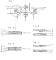
- FIG. 1 shows the top view of conductor tracks with embossed metal structures
- FIG. 2 shows the two substructures in cross section before assembly
- FIG. 3 shows the assembled structure in which a contact is formed from 1 to 3 , 3 a second metal structure without embossing designated.
- the number 2 denotes the transfer film. This can be structured or unstructured.
- the number 4 designates the point at which the contact can be closed, if necessary by suitable measures such as welding, soldering, printing, crimping, riveting, bonding, sintering, reaction welding or reaction joining.
- Numeral 5 shows the possibility of producing the contact 4 by embossing from two opposite sides.
- Numeral 5 denotes a metal structure similar to 3 in Fig. 1, with the difference that it is embossed from below.
- Fig. 4 shows the two structures before joining.
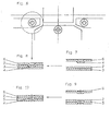
- FIG. 6 shows the conditions when the one metal structure is a system carrier 6 .
- FIG. 7 shows the two substructures in cross section before assembly and
- FIG. 8 correspondingly shows the assembled structure in which a contact from 6 to 3 is formed.
- FIG. 10 shows the possibility is again shown of the contact by stamping two to make opposite sides.
- Fig. 9 shows the two structures before joining.
- FIGS. 11 and 12 show the contacting of the laminate with an electronic component 7 at the contact points 8 provided therefor.
- the number 2 again designates the transfer film.
- the conductor track structure 9 is free of plastic at the contact points. 13 shows the contacted device in cross section.
Landscapes
- Engineering & Computer Science (AREA)
- Manufacturing & Machinery (AREA)
- Microelectronics & Electronic Packaging (AREA)
- Contacts (AREA)
- Combinations Of Printed Boards (AREA)
- Laminated Bodies (AREA)
- Electric Connection Of Electric Components To Printed Circuits (AREA)
Applications Claiming Priority (2)
| Application Number | Priority Date | Filing Date | Title |
|---|---|---|---|
| DE2002105521 DE10205521A1 (de) | 2002-02-08 | 2002-02-08 | Verfahren zur elektrischen Kontaktierung zweier Metallstrukturen |
| DE10205521 | 2002-02-08 |
Publications (2)
| Publication Number | Publication Date |
|---|---|
| EP1335452A2 true EP1335452A2 (fr) | 2003-08-13 |
| EP1335452A3 EP1335452A3 (fr) | 2007-05-02 |
Family
ID=27588519
Family Applications (1)
| Application Number | Title | Priority Date | Filing Date |
|---|---|---|---|
| EP03000900A Withdrawn EP1335452A3 (fr) | 2002-02-08 | 2003-01-16 | Dispostion de mise en contact de deux structures métaliques |
Country Status (5)
| Country | Link |
|---|---|
| EP (1) | EP1335452A3 (fr) |
| CN (1) | CN1437285A (fr) |
| DE (1) | DE10205521A1 (fr) |
| SG (1) | SG108312A1 (fr) |
| TW (1) | TW200302772A (fr) |
Families Citing this family (6)
| Publication number | Priority date | Publication date | Assignee | Title |
|---|---|---|---|---|
| JP2010080318A (ja) * | 2008-09-26 | 2010-04-08 | Smk Corp | コネクタ用シェル |
| DE102010050343A1 (de) * | 2010-11-05 | 2012-05-10 | Heraeus Materials Technology Gmbh & Co. Kg | Chipintegrierte Durchkontaktierung von Mehrlagensubstraten |
| DE102010050342A1 (de) | 2010-11-05 | 2012-05-10 | Heraeus Materials Technology Gmbh & Co. Kg | Laminat mit integriertem elektronischen Bauteil |
| DE102011010186B4 (de) | 2011-02-02 | 2018-10-18 | Heraeus Deutschland GmbH & Co. KG | Verfahren zur Herstellung eines Laminats mit leitender Kontaktierung |
| DE102011122037A1 (de) * | 2011-12-22 | 2013-06-27 | Kathrein-Werke Kg | Verfahren zur Herstellung einer elektrischen Hochfrequenz-Verbindung zwischen zwei Plattenabschnitten sowie eine zugehörige elektrische Hochfrequenz-Verbindung |
| CN104039079B (zh) * | 2013-12-01 | 2017-03-29 | 东莞市震泰电子科技有限公司 | 集成线路板 |
Family Cites Families (9)
| Publication number | Priority date | Publication date | Assignee | Title |
|---|---|---|---|---|
| US3346950A (en) * | 1965-06-16 | 1967-10-17 | Ibm | Method of making through-connections by controlled punctures |
| JP2640780B2 (ja) * | 1989-12-28 | 1997-08-13 | 松下電器産業株式会社 | 金属基板の層間接続方法 |
| JPH06132659A (ja) * | 1992-10-22 | 1994-05-13 | Matsushita Electric Ind Co Ltd | スルホールプリント配線板の製造方法 |
| DE19522338B4 (de) * | 1995-06-20 | 2006-12-07 | Pac Tech-Packaging Technologies Gmbh | Chipträgeranordnung mit einer Durchkontaktierung |
| DE19531970A1 (de) * | 1995-08-30 | 1997-03-06 | Siemens Ag | Verfahren zur Herstellung einer Verbindung zwischen zumindest zwei elektrischen Leitern, von denen einer auf einem Trägersubstrat angeordnet ist |
| JP2831970B2 (ja) * | 1996-04-12 | 1998-12-02 | 山一電機株式会社 | 回路基板における層間接続方法 |
| JP2000151110A (ja) * | 1998-11-13 | 2000-05-30 | Mitsui High Tec Inc | 多層配線基板のビア形成方法及び多層配線基板 |
| DE19852832C2 (de) * | 1998-11-17 | 2001-11-29 | Heraeus Gmbh W C | Verfahren zur Herstellung eines Metall-Kunststoff-Laminats |
| JP3338004B2 (ja) * | 1999-06-25 | 2002-10-28 | 株式会社オートネットワーク技術研究所 | バスバーの接続構造 |
-
2002
- 2002-02-08 DE DE2002105521 patent/DE10205521A1/de not_active Withdrawn
- 2002-12-31 TW TW91138040A patent/TW200302772A/zh unknown
-
2003
- 2003-01-16 EP EP03000900A patent/EP1335452A3/fr not_active Withdrawn
- 2003-01-21 CN CN 03102799 patent/CN1437285A/zh active Pending
- 2003-01-24 SG SG200300165A patent/SG108312A1/en unknown
Also Published As
| Publication number | Publication date |
|---|---|
| SG108312A1 (en) | 2005-01-28 |
| TW200302772A (en) | 2003-08-16 |
| EP1335452A3 (fr) | 2007-05-02 |
| DE10205521A1 (de) | 2003-08-28 |
| CN1437285A (zh) | 2003-08-20 |
Similar Documents
| Publication | Publication Date | Title |
|---|---|---|
| EP1548829B1 (fr) | Module à semi-conducteur de puissance et procédé pour sa fabrication | |
| EP2973671B1 (fr) | Procédé de fabrication d'un composant électronique | |
| WO2012072212A2 (fr) | Composant électronique, procédé pour sa fabrication et plaquette de circuits imprimés comportant un composant électronique | |
| DE102012201172B4 (de) | Verfahren zur Herstellung eines Leistungshalbleitermoduls mit geprägter Bodenplatte | |
| DE102011079708B4 (de) | Trägervorrichtung, elektrische vorrichtung mit einer trägervorrichtung und verfahren zur herstellung dieser | |
| DE112005000952T5 (de) | Elektronik-Modul und Verfahren zur Herstellung desselben | |
| DE102012208146A1 (de) | Verbindungssystem zur herstellung elektrischer verbindungen eines leistungshalbleitermoduls und verfahren zur herstellung solcher verbindungen | |
| DE19522338B4 (de) | Chipträgeranordnung mit einer Durchkontaktierung | |
| DE102017116372B3 (de) | Drucksinterverfahren und Druckübertragungseinrichtung hierfür | |
| WO2002091292A1 (fr) | Procede et demi-produit destines a la fabrication d'une carte a puce comportant une bobine | |
| EP1335452A2 (fr) | Dispostion de mise en contact de deux structures métaliques | |
| DE19852832C2 (de) | Verfahren zur Herstellung eines Metall-Kunststoff-Laminats | |
| EP2954554B1 (fr) | Métallisation multiniveaux sur un substrat en céramique | |
| DE102008058003A1 (de) | Halbleitermodul und Verfahren zu dessen Herstellung | |
| DE19627543B9 (de) | Multi-Layer-Substrat sowie Verfahren zu seiner Herstellung | |
| DE102008040727A1 (de) | Verfahren und Vorrichtung zur Ermittlung der Rotortemperatur einer permanenterregten Synchronmaschine | |
| DE2249209A1 (de) | Leiterrahmen zur verwendung in gehaeusen fuer halbleiterbauelemente | |
| DE2805535A1 (de) | Verfahren zur herstellung einer leitfaehigen verbindung durch eine elektronische leiterplatte | |
| DE2546443C3 (de) | Zusammengesetzte Mikroschaltung und Verfahren zu ihrer Herstellung | |
| DE10225431A1 (de) | Verfahren zur Anschlußkontaktierung von elektronischen Bauelementen auf einem isolierenden Substrat und nach dem Verfahren hergestelltes Bauelement-Modul | |
| DE102017103110B4 (de) | Leistungshalbleitermodul mit einem Schaltungsträger | |
| DE4129835A1 (de) | Leistungselektroniksubstrat und verfahren zu dessen herstellung | |
| EP1085792B1 (fr) | Procédé de fabrication d'un panneau à circuit, et panneau à circuit | |
| DE102005027276B3 (de) | Verfahren zur Herstellung einer Stapelanordnung | |
| DE102006058695A1 (de) | Leistungshalbleitermodul mit stumpf gelötetem Anschlusselement |
Legal Events
| Date | Code | Title | Description |
|---|---|---|---|
| PUAI | Public reference made under article 153(3) epc to a published international application that has entered the european phase |
Free format text: ORIGINAL CODE: 0009012 |
|
| 17P | Request for examination filed |
Effective date: 20030124 |
|
| AK | Designated contracting states |
Designated state(s): AT BE BG CH CY CZ DE DK EE ES FI FR GB GR HU IE IT LI LU MC NL PT SE SI SK TR |
|
| AX | Request for extension of the european patent |
Extension state: AL LT LV MK RO |
|
| RAP1 | Party data changed (applicant data changed or rights of an application transferred) |
Owner name: W.C. HERAEUS GMBH |
|
| PUAL | Search report despatched |
Free format text: ORIGINAL CODE: 0009013 |
|
| AK | Designated contracting states |
Kind code of ref document: A3 Designated state(s): AT BE BG CH CY CZ DE DK EE ES FI FR GB GR HU IE IT LI LU MC NL PT SE SI SK TR |
|
| AX | Request for extension of the european patent |
Extension state: AL LT LV MK RO |
|
| AKX | Designation fees paid |
Designated state(s): AT BE BG CH CY CZ DE DK EE ES FI FR GB GR HU IE IT LI LU MC NL PT SE SI SK TR |
|
| STAA | Information on the status of an ep patent application or granted ep patent |
Free format text: STATUS: THE APPLICATION IS DEEMED TO BE WITHDRAWN |
|
| 18D | Application deemed to be withdrawn |
Effective date: 20071103 |