EP1335532B1 - Digital-/Analogkonverter mit Zeit-Dithering zum Ausblenden von Audiotönen - Google Patents
Digital-/Analogkonverter mit Zeit-Dithering zum Ausblenden von Audiotönen Download PDFInfo
- Publication number
- EP1335532B1 EP1335532B1 EP03002972A EP03002972A EP1335532B1 EP 1335532 B1 EP1335532 B1 EP 1335532B1 EP 03002972 A EP03002972 A EP 03002972A EP 03002972 A EP03002972 A EP 03002972A EP 1335532 B1 EP1335532 B1 EP 1335532B1
- Authority
- EP
- European Patent Office
- Prior art keywords
- clock
- modulated signal
- modulator
- time
- signal
- Prior art date
- Legal status (The legal status is an assumption and is not a legal conclusion. Google has not performed a legal analysis and makes no representation as to the accuracy of the status listed.)
- Expired - Lifetime
Links
- 230000009467 reduction Effects 0.000 claims description 84
- 230000007704 transition Effects 0.000 claims description 32
- 238000004891 communication Methods 0.000 claims description 29
- 238000000034 method Methods 0.000 claims description 19
- 230000005236 sound signal Effects 0.000 claims description 19
- 238000007493 shaping process Methods 0.000 claims description 12
- 238000001914 filtration Methods 0.000 claims description 7
- 238000010586 diagram Methods 0.000 description 34
- 239000000306 component Substances 0.000 description 23
- 108091006146 Channels Proteins 0.000 description 11
- 230000004044 response Effects 0.000 description 10
- 239000000872 buffer Substances 0.000 description 9
- 230000008569 process Effects 0.000 description 7
- 238000003860 storage Methods 0.000 description 6
- 230000005540 biological transmission Effects 0.000 description 5
- 230000001413 cellular effect Effects 0.000 description 5
- 238000006243 chemical reaction Methods 0.000 description 5
- 230000003993 interaction Effects 0.000 description 4
- 238000012546 transfer Methods 0.000 description 4
- 230000008901 benefit Effects 0.000 description 3
- 230000001360 synchronised effect Effects 0.000 description 3
- 239000006227 byproduct Substances 0.000 description 2
- 230000006835 compression Effects 0.000 description 2
- 238000007906 compression Methods 0.000 description 2
- 230000010354 integration Effects 0.000 description 2
- 238000004519 manufacturing process Methods 0.000 description 2
- 238000012986 modification Methods 0.000 description 2
- 230000004048 modification Effects 0.000 description 2
- 230000006855 networking Effects 0.000 description 2
- 101150093547 AUX1 gene Proteins 0.000 description 1
- 235000008694 Humulus lupulus Nutrition 0.000 description 1
- 101100367246 Saccharomyces cerevisiae (strain ATCC 204508 / S288c) SWA2 gene Proteins 0.000 description 1
- 230000003044 adaptive effect Effects 0.000 description 1
- 230000002238 attenuated effect Effects 0.000 description 1
- 230000000903 blocking effect Effects 0.000 description 1
- 230000015556 catabolic process Effects 0.000 description 1
- 230000000295 complement effect Effects 0.000 description 1
- 239000002131 composite material Substances 0.000 description 1
- 239000008358 core component Substances 0.000 description 1
- 238000012937 correction Methods 0.000 description 1
- 239000013078 crystal Substances 0.000 description 1
- 238000006731 degradation reaction Methods 0.000 description 1
- 230000003111 delayed effect Effects 0.000 description 1
- 230000001419 dependent effect Effects 0.000 description 1
- 230000000994 depressogenic effect Effects 0.000 description 1
- 230000000694 effects Effects 0.000 description 1
- 238000009499 grossing Methods 0.000 description 1
- 238000005304 joining Methods 0.000 description 1
- 230000010355 oscillation Effects 0.000 description 1
- 230000002093 peripheral effect Effects 0.000 description 1
- 238000012545 processing Methods 0.000 description 1
- 238000013139 quantization Methods 0.000 description 1
- 238000005070 sampling Methods 0.000 description 1
- 230000003068 static effect Effects 0.000 description 1
- 238000012360 testing method Methods 0.000 description 1
- 230000002087 whitening effect Effects 0.000 description 1
Images






Classifications
-
- H—ELECTRICITY
- H04—ELECTRIC COMMUNICATION TECHNIQUE
- H04W—WIRELESS COMMUNICATION NETWORKS
- H04W88/00—Devices specially adapted for wireless communication networks, e.g. terminals, base stations or access point devices
- H04W88/02—Terminal devices
- H04W88/06—Terminal devices adapted for operation in multiple networks or having at least two operational modes, e.g. multi-mode terminals
-
- H—ELECTRICITY
- H03—ELECTRONIC CIRCUITRY
- H03M—CODING; DECODING; CODE CONVERSION IN GENERAL
- H03M3/00—Conversion of analogue values to or from differential modulation
- H03M3/30—Delta-sigma modulation
- H03M3/322—Continuously compensating for, or preventing, undesired influence of physical parameters
- H03M3/324—Continuously compensating for, or preventing, undesired influence of physical parameters characterised by means or methods for compensating or preventing more than one type of error at a time, e.g. by synchronisation or using a ratiometric arrangement
- H03M3/326—Continuously compensating for, or preventing, undesired influence of physical parameters characterised by means or methods for compensating or preventing more than one type of error at a time, e.g. by synchronisation or using a ratiometric arrangement by averaging out the errors
- H03M3/328—Continuously compensating for, or preventing, undesired influence of physical parameters characterised by means or methods for compensating or preventing more than one type of error at a time, e.g. by synchronisation or using a ratiometric arrangement by averaging out the errors using dither
- H03M3/3283—Continuously compensating for, or preventing, undesired influence of physical parameters characterised by means or methods for compensating or preventing more than one type of error at a time, e.g. by synchronisation or using a ratiometric arrangement by averaging out the errors using dither the dither being in the time domain
-
- H—ELECTRICITY
- H03—ELECTRONIC CIRCUITRY
- H03M—CODING; DECODING; CODE CONVERSION IN GENERAL
- H03M7/00—Conversion of a code where information is represented by a given sequence or number of digits to a code where the same, similar or subset of information is represented by a different sequence or number of digits
- H03M7/30—Compression; Expansion; Suppression of unnecessary data, e.g. redundancy reduction
- H03M7/3002—Conversion to or from differential modulation
- H03M7/3004—Digital delta-sigma modulation
- H03M7/3006—Compensating for, or preventing of, undesired influence of physical parameters
- H03M7/3008—Compensating for, or preventing of, undesired influence of physical parameters by averaging out the errors, e.g. using dither
-
- H—ELECTRICITY
- H03—ELECTRONIC CIRCUITRY
- H03M—CODING; DECODING; CODE CONVERSION IN GENERAL
- H03M3/00—Conversion of analogue values to or from differential modulation
- H03M3/30—Delta-sigma modulation
- H03M3/322—Continuously compensating for, or preventing, undesired influence of physical parameters
- H03M3/324—Continuously compensating for, or preventing, undesired influence of physical parameters characterised by means or methods for compensating or preventing more than one type of error at a time, e.g. by synchronisation or using a ratiometric arrangement
- H03M3/326—Continuously compensating for, or preventing, undesired influence of physical parameters characterised by means or methods for compensating or preventing more than one type of error at a time, e.g. by synchronisation or using a ratiometric arrangement by averaging out the errors
- H03M3/328—Continuously compensating for, or preventing, undesired influence of physical parameters characterised by means or methods for compensating or preventing more than one type of error at a time, e.g. by synchronisation or using a ratiometric arrangement by averaging out the errors using dither
- H03M3/3287—Continuously compensating for, or preventing, undesired influence of physical parameters characterised by means or methods for compensating or preventing more than one type of error at a time, e.g. by synchronisation or using a ratiometric arrangement by averaging out the errors using dither the dither being at least partially dependent on the input signal
-
- H—ELECTRICITY
- H03—ELECTRONIC CIRCUITRY
- H03M—CODING; DECODING; CODE CONVERSION IN GENERAL
- H03M3/00—Conversion of analogue values to or from differential modulation
- H03M3/30—Delta-sigma modulation
- H03M3/322—Continuously compensating for, or preventing, undesired influence of physical parameters
- H03M3/324—Continuously compensating for, or preventing, undesired influence of physical parameters characterised by means or methods for compensating or preventing more than one type of error at a time, e.g. by synchronisation or using a ratiometric arrangement
- H03M3/326—Continuously compensating for, or preventing, undesired influence of physical parameters characterised by means or methods for compensating or preventing more than one type of error at a time, e.g. by synchronisation or using a ratiometric arrangement by averaging out the errors
- H03M3/328—Continuously compensating for, or preventing, undesired influence of physical parameters characterised by means or methods for compensating or preventing more than one type of error at a time, e.g. by synchronisation or using a ratiometric arrangement by averaging out the errors using dither
- H03M3/33—Continuously compensating for, or preventing, undesired influence of physical parameters characterised by means or methods for compensating or preventing more than one type of error at a time, e.g. by synchronisation or using a ratiometric arrangement by averaging out the errors using dither the dither being a random signal
- H03M3/332—Continuously compensating for, or preventing, undesired influence of physical parameters characterised by means or methods for compensating or preventing more than one type of error at a time, e.g. by synchronisation or using a ratiometric arrangement by averaging out the errors using dither the dither being a random signal in particular a pseudo-random signal
-
- H—ELECTRICITY
- H03—ELECTRONIC CIRCUITRY
- H03M—CODING; DECODING; CODE CONVERSION IN GENERAL
- H03M3/00—Conversion of analogue values to or from differential modulation
- H03M3/30—Delta-sigma modulation
- H03M3/39—Structural details of delta-sigma modulators, e.g. incremental delta-sigma modulators
- H03M3/412—Structural details of delta-sigma modulators, e.g. incremental delta-sigma modulators characterised by the number of quantisers and their type and resolution
- H03M3/422—Structural details of delta-sigma modulators, e.g. incremental delta-sigma modulators characterised by the number of quantisers and their type and resolution having one quantiser only
- H03M3/43—Structural details of delta-sigma modulators, e.g. incremental delta-sigma modulators characterised by the number of quantisers and their type and resolution having one quantiser only the quantiser being a single bit one
-
- H—ELECTRICITY
- H03—ELECTRONIC CIRCUITRY
- H03M—CODING; DECODING; CODE CONVERSION IN GENERAL
- H03M3/00—Conversion of analogue values to or from differential modulation
- H03M3/30—Delta-sigma modulation
- H03M3/39—Structural details of delta-sigma modulators, e.g. incremental delta-sigma modulators
- H03M3/436—Structural details of delta-sigma modulators, e.g. incremental delta-sigma modulators characterised by the order of the loop filter, e.g. error feedback type
- H03M3/456—Structural details of delta-sigma modulators, e.g. incremental delta-sigma modulators characterised by the order of the loop filter, e.g. error feedback type the modulator having a first order loop filter in the feedforward path
-
- H—ELECTRICITY
- H03—ELECTRONIC CIRCUITRY
- H03M—CODING; DECODING; CODE CONVERSION IN GENERAL
- H03M3/00—Conversion of analogue values to or from differential modulation
- H03M3/30—Delta-sigma modulation
- H03M3/50—Digital/analogue converters using delta-sigma modulation as an intermediate step
-
- H—ELECTRICITY
- H03—ELECTRONIC CIRCUITRY
- H03M—CODING; DECODING; CODE CONVERSION IN GENERAL
- H03M7/00—Conversion of a code where information is represented by a given sequence or number of digits to a code where the same, similar or subset of information is represented by a different sequence or number of digits
- H03M7/30—Compression; Expansion; Suppression of unnecessary data, e.g. redundancy reduction
- H03M7/3002—Conversion to or from differential modulation
- H03M7/3004—Digital delta-sigma modulation
- H03M7/3015—Structural details of digital delta-sigma modulators
- H03M7/302—Structural details of digital delta-sigma modulators characterised by the number of quantisers and their type and resolution
- H03M7/3024—Structural details of digital delta-sigma modulators characterised by the number of quantisers and their type and resolution having one quantiser only
- H03M7/3028—Structural details of digital delta-sigma modulators characterised by the number of quantisers and their type and resolution having one quantiser only the quantiser being a single bit one
-
- H—ELECTRICITY
- H03—ELECTRONIC CIRCUITRY
- H03M—CODING; DECODING; CODE CONVERSION IN GENERAL
- H03M7/00—Conversion of a code where information is represented by a given sequence or number of digits to a code where the same, similar or subset of information is represented by a different sequence or number of digits
- H03M7/30—Compression; Expansion; Suppression of unnecessary data, e.g. redundancy reduction
- H03M7/3002—Conversion to or from differential modulation
- H03M7/3004—Digital delta-sigma modulation
- H03M7/3015—Structural details of digital delta-sigma modulators
- H03M7/3031—Structural details of digital delta-sigma modulators characterised by the order of the loop filter, e.g. having a first order loop filter in the feedforward path
- H03M7/3033—Structural details of digital delta-sigma modulators characterised by the order of the loop filter, e.g. having a first order loop filter in the feedforward path the modulator having a higher order loop filter in the feedforward path, e.g. with distributed feedforward inputs
- H03M7/304—Structural details of digital delta-sigma modulators characterised by the order of the loop filter, e.g. having a first order loop filter in the feedforward path the modulator having a higher order loop filter in the feedforward path, e.g. with distributed feedforward inputs with distributed feedback, i.e. with feedback paths from the quantiser output to more than one filter stage
-
- H—ELECTRICITY
- H04—ELECTRIC COMMUNICATION TECHNIQUE
- H04W—WIRELESS COMMUNICATION NETWORKS
- H04W84/00—Network topologies
- H04W84/02—Hierarchically pre-organised networks, e.g. paging networks, cellular networks, WLAN [Wireless Local Area Network] or WLL [Wireless Local Loop]
- H04W84/10—Small scale networks; Flat hierarchical networks
- H04W84/12—WLAN [Wireless Local Area Networks]
Definitions
- the present invention relates to communications; and more particularly to signal conversion in wireless communication devices that service voice communications.
- Bluetooth Specification enables the creation of small personal area networks (PAN's), where the typical operating range of a device is 100 meters or less.
- PAN personal area networks
- Bluetooth devices sharing a common channel sequence form a piconet.
- the Bluetooth Specification supports voice communications between Bluetooth enabled devices.
- the voice communications must be wirelessly supported in a continuous fashion so that carried voice signals are of an acceptable quality.
- Unexpected gaps, e.g., dropped packets, on the wireless link between supported Bluetooth devices causes degradation in the voice communication resulting in popping, static, or other unpleasant audible event. This problem is especially troublesome with Bluetooth devices since, in some operations, the communication link will regularly drop packets that carry the voice signals.
- a further shortcoming of such operations relates to the manner in which packetized audio data is transmitted between Bluetooth devices.
- a first Bluetooth device transmits packetized audio data to a second Bluetooth device for presentation to a user.
- the Bluetooth WLAN supports data rates greatly in excess of those required for satisfactory voice service
- each transmission from the first Bluetooth device carries a relatively large amount of packetized audio data.
- the duration of this transmission is typically small compared to the duration over which the second Bluetooth device will present the packetized audio data (carried in the transmission) to the user.
- the second Bluetooth device buffers the received packetized audio data and presents the packetized audio data (in a converted form) over an appropriate time period.
- the packetized audio data stored in the input buffer is fully consumed prior to receipt of another transmission from the first Bluetooth device, it will appear to the second Bluetooth device that packetized audio data is lost (or severely delayed), and the second Bluetooth device will provided degraded audio to the serviced user.
- Bluetooth (and other wireless) devices that service voice communications include Analog to Digital Converters (ADCs) and Digital to Analog Converters (DACs).
- ADCs Analog to Digital Converters
- DACs Digital to Analog Converters
- the ADC of the wireless device receives an analog audio signal from a coupled microphone and converts the analog audio signal to a digital audio signal. During this conversion process, the ADC may introduce "tones" that are a byproduct of the sampling characteristics of the ADC.
- the DAC receives a digital audio signal and converts the digital audio signal to an analog audio signal that it applies to coupled to a speaker.
- the DAC may introduce “tones" to the analog audio signal that are a byproduct of the conversion process. These "tones,” while having a relatively small magnitude compared to an active signal are noticeable during “quiet” times.
- “quiet” times exist when no input is provided to the microphone.
- “quiet” times exist when data is lost or when incoming data contains no audio data.
- WO 99/49578 describes a DAC system wherein a dither signal, which is preferably a square wave, from a signal generator is added to the output of a digital filter at a summer.
- the composite multi-bit signal is fed to the delta-sigma modulator for noise-shaping and outputting as a single bit signal from the digital section.
- the single bit signal is input to the analog section including a DAC and an analog filter.
- the noise shaping property of the delta-sigma modulation tends to shift any spurious noises to higher frequencies outside the passband of the system where they are readily attenuated through filtering.
- EP 0 660 222 describes a data converter for converting a signal either from analog form to digital form or from digital form to analog form which includes a storage register.
- the storage register receives and temporarily stores digital data samples.
- the digital data samples are transferable out of the storage register in the same sequence in which they were received.
- a digital signal processor coupled to the storage register is interruptible to transfer digital data samples either to or from the storage register. In this manner, the digital signal processor transfers multiple digital data samples either to or from the storage register during each interrupt rather than transferring a single data sample per interrupt, thereby reducing the number of interrupts necessary to transfer a given number of digital data samples.
- WLAN Wireless Local Area Network
- a DAC constructed according to the present invention converts digital data to an analog signal.
- the DAC includes an interpolation filter, a modulator, and a time dither clock reduction circuit.
- the interpolation filter receives the digital data and interpolates and filters the digital data to produce an interpolated and filtered digital signal.
- the modulator receives the interpolated and filtered digital signal and a feedback signal. The modulator modulates the interpolated and filtered digital signal based upon the feedback signal to produce a modulated signal at a modulator clock rate.
- the time dither clock reduction circuit receives the modulated signal and applies both clock reduction and time dithering to the modulated signal to produce a time dithered/clock reduced modulated signal.
- the time dithered/clock reduced modulated signal serves as the analog signal and also serves as the feedback signal.
- the time dithering clock reduction circuit At each modulator clock cycle, the time dithering clock reduction circuit considers modulated signals for a dithering factor, N, previous modulator clock cycles and the modulated signal for a current modulator clock cycle. If at least one constraint is satisfied for the N previous modulator clock cycles, the time dithering clock reduction circuit transitions the time dithered/clock reduced modulated signal with the modulated signal.
- the time dithering clock reduction circuit transitions the time dithered/clock reduced modulated signal from one to zero.
- the time dithering clock reduction circuit holds the time dithered/clock reduced modulated signal at one.
- the time dithering clock reduction circuit transitions the time dithered/clock reduced modulated signal from zero to one.
- the time dithering clock reduction circuit holds the time dithered/clock reduced modulated signal at zero.
- a new dithering factor, N may be selected.
- the new dithering factor is determined by generating a random number and selecting the new dithering factor based upon a comparison of the random number to at least one constraint.
- the DAC of the present invention may be contained within a wireless local area network (WLAN) transceiving integrated circuit that services voice communications in a WLAN with at least one other WLAN device.
- WLAN transceiving integrated circuit in one embodiment, is formed as a single monolithic integrated circuit.
- audio communications and “voice communications” are both be used to refer to communications that contain information based upon audio signals that originate from or that are presented to a user in an audio format.
- voice/audio communications need not be received directly from a human but may be generated by electronic equipment such as computers, media players, etc.
- the WLAN transceiving integrated circuit may operate consistently with the Bluetooth Specification or with another standard, e.g., IEEE 802.11(a), IEEE 802.11(b), IEEE 802.11(c), etc.
- the WLAN transceiving integrated circuit operates within a Bluetooth WLAN, the WLAN transceiving integrated circuit supports the Bluetooth Specification. In such case, the WLAN transceiving integrated circuit transmits packetized audio data to other Bluetooth devices and receives packetized audio data from other Bluetooth devices.
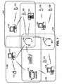
- FIG. 1 is a system diagram illustrating a plurality of Wireless Local Area Network (WLAN) devices, some of which have installed therein WLAN transceiving integrated circuit constructed according to the present invention. Each of these WLAN devices supports one or more versions of the Bluetooth Specification.
- a Bluetooth "scatternet" is formed from multiple "piconets" with overlapping coverage.
- the scatternet of FIG. 1 includes four separate piconets 102, 104, 106, and 108.
- Piconet 102 includes master (computer) 110, slave 112 (PDA), slave 114 (printer), slave 130 (wireless headset), and slave 115 (music source).
- PDA slave 112
- slave 114 printer
- slave 130 wireless headset
- slave 115 music source
- Piconet 104 includes master 120 (computer), slave 122 (PDA), slave 123 (wireless phone), slave 130 (wireless headset), and slave 134 (landline phone).
- Piconet 106 includes master (computer) 116, slave 118 (PDA), slave 114 (printer), slave 130 (wireless headset), and slave 132 (wireless headset).
- Piconet 108 includes master (computer) 124, slave 126 (PDA), slave 128 (wireless phone, e.g., WLAN phone, cell phone, etc.), slave 132 (wireless headset), and slave 130 (wireless headset).
- the four separate piconets 102, 104, 106, and 108 have overlapping coverage areas. In the embodiment of FIG.
- the scatternet of FIG. 1 may service a call center, customer service department, or other office environment, for example that benefits by the wireless interconnection of the illustrated devices.
- a user of wireless headset 130 may establish communications with any WLAN device in a piconet of which the wireless headset 130 (or 132) is also a member.
- the wireless headset 130 may have a minimal user interface, e.g., a single authenticate button that initiates joining of a piconet.
- the wireless headset 130 in its operating location, resides within the service coverage area of each of the four separate piconets 102, 104, 106, and 108 that form the scatternet.
- a user of the wireless headset 130 depresses an authenticate button to start the authentication process.
- the wireless headset attempts to join one of piconets 102, 104, 106, and 108. Subsequent authentication operations are required to have the wireless headset join the selected piconet. These subsequent authentication operations may include prompting the user for selection of the piconet, requiring that entry be made on the home computer 110 to allow the wireless headset 130 to join the piconet 102, or other authentication operations. Likewise, the wireless headset 132 joins piconet 106 by performing appropriate authentication operations with master (computer 116) of piconet 106.
- a wireless headset e.g., 130 or 132 joins a respective piconet, 102 or 106
- the wireless headset establishes an audio link with one or more of the members of the piconet via respective WLAN links.
- an attendant using the wireless headset 130 services calls of the call center. Such calls will be received and managed by the computer 110 in the example.
- the user of wireless headset 132 will work in conjunction with the computer 116 to service calls for the call center.
- Each of the WLAN devices illustrated in FIG. 1 may include a WLAN transceiving integrated circuit constructed according to the present invention.
- the WLAN transceiving integrated circuit gracefully operates when RF slots of a transmitting WLAN device servicing as a master of a piconet are not synchronized with the other operations of the WLAN transceiving integrated circuit.
- PCM audio data that is produced by the WLAN transceiving integrated circuit based upon received packetized audio data is substantially temporally aligned with RF slots of the transmitting WLAN device.
- the WLAN device at the same rate consumes packetized audio data as it is received from the transmitting WLAN device.
- the PCM audio data output does not surge ahead of, or lag behind, the packetized audio data that is received from the transmitting WLAN device.
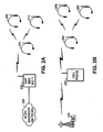
- FIG. 2A is a system diagram illustrating the interaction between a plurality of WLAN devices 204, 208, and 210 constructed according to the present invention and a Wireless Access Point (WAP) 202.
- the wireless headset 204 is Bluetooth compliant and/or IEEE 802.11 compliant, e.g., IEEE 802.11a, IEEE 802.11b, IEEE 802.11g, etc.
- the wireless headset 204 establishes a voice communication via the WAP 202 with another device also serviced by the WAP 202, or, more likely, with another device couple to the WAP 202 via the Wireless Local Area Network (WLAN) backbone network 206.
- the wireless headset 204 services voice communications with two additional wireless headsets 208 and 210.
- FIG. 2B is a system diagram illustrating the interaction between wireless headsets 254, 258, and 260, a cell phone 252, and a cellular base station 256.
- the cell phone 252 establishes a cellular telephone call via the base station 256 with another wireless device or with a wired device that couples to the base station 256 via a wired connection.
- the cell phone 252 operates according to a cellular operating standard, e.g., IS-95A, IS-95B, IS-136, GSM, 1xRTT, 1xEV, UMTS, etc.
- the cell phone 252 also supports the Bluetooth specification and communications with the wireless headset 254 via Bluetooth operations.
- the wireless headset 254 supports communications with wireless headsets 258 and 260 also via the Bluetooth operations.
- the user of the wireless headset 254 while operating a vehicle may use the wireless headset 254 for audio communications serviced by the cell phone 252.
- usage of the components of FIG. 2B is not limited to a vehicular application.
- the wireless headset 254 supports conferencing with wireless headsets 258 and 260.
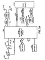
- FIG. 3A is a block diagram illustrating the electrical components of a wireless headset that includes a first embodiment of a WLAN transceiving integrated circuit constructed according to the present invention.
- the wireless headset includes the WLAN transceiving integrated circuit 300 and a number of supporting components.
- the Radio Frequency (RF) interface for the WLAN transceiving integrated circuit 300 includes a Power Amplifier (PA) 302, a Receive/Transmit switch 304, and an antenna 306.
- the power supply for wireless headset is a battery 334 that couples to the WLAN transceiving integrated circuit 300 and also couples to other components of the wireless headset.
- the WLAN transceiving integrated circuit 300 includes a plurality of interfaces that adhere to standardized interface formats.
- a Pulse Code Modulated (PCM) connection 310 couples the WLAN transceiving integrated circuit 300 to an audio Coder-Decoder (CODEC) 314 that performs coding/decoding operations.
- the PCM connection 310 includes a PCM synchronization signal, F S .
- the audio CODEC 314 couples to a microphone 316 and to a speaker 318.
- a serial I/O 320 may couple the WLAN transceiving integrated circuit 300 to an external host 320. However, in the embodiment of FIG. 3 , the wireless headset does not require an external host 320.
- a parallel I/O 324 may couple the WLAN transceiving integrated circuit 300 to a PCMCIA controller 326 and to a USB controller 330 that my also couple the WLAN transceiving integrated circuit 300 to the external host 320 via a PCMCIA bus 328 and a USB bus 332, respectively.
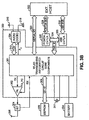
- FIG. 3B is a block diagram illustrating the electrical components of a wireless headset that includes a second embodiment of a WLAN transceiving integrated circuit constructed according to the present invention.
- the embodiment of FIG. 3B is similar to the embodiment of FIG. 3A except that the embodiment of FIG. 3B includes additional integration.
- the PA 352 and audio CODEC 364 are on-chip and the remaining components of the WLAN transceiving integrated circuit are referred to as WLAN transceiving integrated circuit core components 351.
- the WLAN transceiving integrated circuit includes an on-chip local oscillator and does not require an external crystal to provide a reference oscillation 311.
- FIG. 4A is a block diagram generally illustrating the components of a WLAN transceiving integrated circuit constructed according to the present invention.
- the baseband processor 400 includes a radio transceiver 402, a baseband core (BBC) 404, and a PCM interface 406.
- the WLAN transceiving integrated circuit 400 shown in FIG. 4A has an integrated radio transceiver 402 that has been optimized for use in 2.4 GHz Bluetooth wireless systems.
- the BBC 404 implements the physical layer of the Bluetooth interface with other Bluetooth enabled WLAN devices.
- the BBC 404 manages physical channels and links apart from other services like error correction, data whitening, hop selection and Bluetooth security.
- the BBC 404 implements the physical layer lies on top of the Bluetooth radio layer in the Bluetooth protocol stack.
- the baseband protocol is implemented as a Link Controller, which works with the link manager for carrying out link level routines like link connection and power control.
- the BBC 404 also manages asynchronous and synchronous links, handles packets and does paging and inquiry to access and inquire Bluetooth devices in the area.
- the baseband transceiver 400 applies a time-division duplex (TDD) scheme (alternate transmit and receive). Therefore apart from different hopping frequency (frequency division), the time is also slotted.
- TDD time-division duplex
- the BBC 404 supports 13 different packet types for the baseband layer of the Bluetooth system. All higher layers use these packets to compose higher level PDU's.
- the packets are ID, NULL, POLL, FHS, and DM1. These packets are defined for both SCO and ACL links.
- DH1, AUX1, DM3, DH3, DM5, DH5 packets are defined for ACL links only.
- HV1, HV2, HV3, and DV packets are defined for SCO links only.
- Each Bluetooth packet consists of 3 entities, an access code (68/72 bits), a header (54 bits), and a payload (0-2745 bits). The Access code is used for timing synchronization, offset compensation, paging and inquiry.
- Access codes There are three different types of Access codes: (1) the Channel Access Code (CAC); (2) the Device Access Code (DAC); and (3) the Inquiry Access Code (IAC).
- CAC Channel Access Code
- DAC Device Access Code
- IAC Inquiry Access Code
- the channel access code identifies a unique piconet while the DAC is used for paging and its responses.
- the IAC is used for inquiry purpose.
- the header contains information for packet acknowledgement, packet numbering for out-of-order packet reordering, flow control, slave address and error check for header.
- the Payload contains a voice field, a data field or both. If the payload is a data field, the payload will also contain a payload header.
- packetized audio data is carried between WLAN devices in Bluetooth Specification Synchronous Connection Oriented (SCO) data packets.
- SCO Bluetooth Specification Synchronous Connection Oriented
- the PCM I/F 406 couples to the baseband core 404 and produces PCM audio data and also a PCM synchronization signal, F S .
- the PCM synchronization signal, F S is temporally aligned with RF slots of the radio transceiver 402 that are produced by a servicing master WLAN device.
- the PCM I/F 406 may receive the PCM synchronization signal, F S , directly from the baseband core 404 or may construct the PCM synchronization signal, F S , based upon a synchronization signal received from either/both of the radio transceiver 402 or/and the baseband core 404.
- FIG. 4B is a block diagram generally illustrating in more detail the components of the WLAN transceiving integrated circuit 450 constructed according to the present invention of FIG. 4A .
- the radio transceiver 454 has been designed to provide low-power, low-cost, robust communications for applications operating in the globally available 2.4 GHz unlicensed ISM band. It is fully compliant with the Bluetooth RF specification Version 1.1 and meets or exceeds the requirements to provide the highest communication link quality service.
- the radio transceiver 454 has a high-degree of linearity, an extended dynamic range, and high order on-chip channel filtering to ensure reliable operation in the noisy 2.4 GHz ISM band.
- the performance of the receiver chain is reflected in the IP3, co-channel interference, and out-of-band blocking specifications.
- the radio transceiver 402 includes a fully integrated transmitter.
- Baseband data received from the baseband core 404 is GFSK modulated and up-converted to the 2.4 GHz ISM band via an internal mixer.
- the radio transceiver 454 provides a normal power output of 0 dBm and has a power control signal provided by the WLAN transceiving integrated circuit 300 that controls the PA 302 to provide 24 dBm of gain control in 8 dBm step size.
- the radio transceiver 454 interfaces with the BBC 452 via a radio transceiver interface 456, a Local Oscillator (LO) 458, and a Received Signal Strength Indicator (RSSI) 460.
- the LO 458 provides fast frequency hopping (1600 hops/second) across the 79 maximum available Bluetooth channels.
- the radio transceiver 454 of the WLAN transceiving integrated circuit 400 features on-chip calibration, eliminating process variation across components. This enables the WLAN transceiving integrated circuit 450 to be used in high volume applications.
- the WLAN transceiving integrated circuit 450 parallel I/O interface 324 (coupled to the BBC 452 via an I/O port 464) can be operated in either Master or Slave mode. By default the WLAN transceiving integrated circuit 400 will power up in one of the modes depending on the setting of MODE pins (not shown). In Master mode, the WLAN transceiving integrated circuit 450 accesses peripheral devices on the parallel bus 324 in (1) 8-bit parallel I/O Normal A0 Read and Write modes; and (2) 8-bit parallel I/O Fast ALE Read and Write modes. In Slave mode, the parallel I/O bus interface 464 is intended to support a connection to a wide range of external host processors or external host controllers.
- the Slave mode interface timing of the parallel bus 324 can be in one of: (1) 8-bit parallel I/O Normal A0 Read and Write modes; (2) 8-bit parallel I/O Fast A0 Read and Write modes; and (3) 8-bit parallel I/O Fast ALE Read and Write modes.
- the asynchronous serial interface I/O 320 (coupled to the BBC 452 via an asynchronous serial port 462) enables an asynchronous serial data stream to communicate with the BBC 452 in a similar fashion as the slave mode parallel I/O interface.
- a programmable baud rate generator is provided to select, transmit and receive clock rates from 9600 bps to 921.6 Kbps. The default baud rate is determined by the setting of external selection pins BAUD[3:0] (not shown).
- a master mode 2-wire serial interface bus is available on the WLAN transceiving integrated circuit 450 to allow read and write operations from/to an I2C serial EEPROM 309 via the I2C interface 466 and the I2C connection 468.
- the BBC 452 via software instruction at power-on reset, sets the control of the I2C pins.
- the boot code that resides on the BBC 452 on-chip boot ROM monitors a controlled pin to determine the presence or absence of the serial EEPROM 309. If an EEPROM 309 is detected, the BBC 452 on chip boot code performs read operations from the EEPROM 309 that contains the fully operational microcode for the BBC 452. If the EEPROM 309 is not present, the BBC 452 expects the microcode to be downloaded from the external host.
- the BBC 452 implements all the high-level time critical Link Management functions in dedicated hardware under the control of the micro-sequencer.
- the BBC 452 hardware processes Bluetooth Link Control (LC) functions and manages Bluetooth slot usage.
- the external host 322 can use this register to manipulate the device pins in order to read and modify the EEPROM 309 contents as desired.
- the WLAN transceiving integrated circuit further includes power management functions 474 and Built-In-Self Test 472 functions.
- the power management unit 474 provides power management features that are controlled through setting of the power management registers.
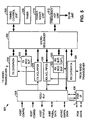
- FIG. 5 is a block diagram illustrating the components of a Baseband Core (BBC) 550 of the WLAN transceiving integrated circuit constructed according to the present invention of FIGs. 4A and 4B .
- the BBC 550 includes a microsequencer (processor) 502, a timing control unit 506, a timer 508, a power management unit 510, and a frequency hop unit 512.
- the BBC 404 includes a TX data path 514 that couples to the radio transceiver, a TX SCO buffer (output buffer) 516, and TX ACL FIFOs 518.
- the BBC 550 includes an RX data path 524 that couples to the radio transceiver, an RX SCO input buffer 522, and an RX ACL FIFO 520. These components service the receive path for the BBC 550.
- the registers/buffers 504 receive external host configuration data, external host command data, provide status to the external host, and interface with the external host via the parallel and serial buses.
- the registers/buffers 504 also interface with the audio CODEC 314 via a PCM interface 406.
- An input buffer controller 523 operably couples to the input buffer 522 and to the processor 502.
- FIG. 6 is a block diagram generally illustrating the components of a Pulse Code Modulated (PCM) interface 406 of the Baseband Core 550 of FIG. 5 .
- the PCM interface 406 includes a transcoder 602 having a decoder 608 and an encoder 610, a switch box 604 and an audio CODEC 314. Coupled to the audio CODEC 314 are a speaker 318 and a microphone 316.
- the audio CODEC 314 includes a Digital-to-Analog-Converter (DAC) 614 that converts PCM audio data to an analog audio signal and provides the analog audio signal to a speaker 318.
- the audio CODEC 314 includes an Analog-to-Digital-Converter (ADC) 614 that receives an analog audio signal from the coupled microphone 316 and converts the analog audio signal to PCM audio data.
- ADC Analog-to-Digital-Converter
- the transcoder 602 converts packetized audio data (encoded) that is suitable for the WLAN interface to PCM audio data that is suitable for the audio CODEC 314, and vice versa.
- the decoder 608 converts encoded packetized audio data to PCM audio data while the encoder 610 converts PCM audio data to encoded packetized audio data.
- the transcoder 602 supports 13-bit linear PCM CODEC devices with a 2's complement serial data format. It is capable of supporting an external audio clock or outputting an audio clock (ACLK) in multiples of 128 KHz, from 128 KHz to 4096 KHz.
- ACLK audio clock
- the PCM I/F 406 can generate PCM audio data in an 8 KHz short/long Frame Sync (ASYNC) format. In an audio slave mode, the PCM I/F 406 can receive PCM audio data in an 8 KHz short Frame Sync format.
- ASYNC 8 KHz short/long Frame Sync
- the PCM I/F 406 supports up to three SCO channels, and in at least one embodiment, the PCM audio data is Time Division Multiplexed (TDM) into slots within every ASYNC period. Each of the three SCO channels can be assigned to any TDM slot.
- the TDM slots can be programmed from one to 16 slots depending on the ACLK rate.
- the two additional SCO channels are available using GPIO6 and GPIO7 as the PCM Frame Sync signals (i.e., ASYNC3 and ASYNC2, respectively).
- the transcoder 602 can process each SCO channel with A-law operations, ⁇ -law operations, or Continuous Variable Slope Delta (CVSD) operations.
- the appropriate voice-coding scheme is selected after negotiations between the Link Managers of the communicating WLAN devices.
- On the Bluetooth air-interface either a 64 kb/s log PCM format (A-law or ⁇ -law) is used, or a 64 kb/s CVSD is used.
- the latter format applies an adaptive delta modulation algorithm with syllabic companding.
- the voice coding on the PCM I/F 406 should have a quality equal to or better than the quality of 64 kb/s log PCM.
- the voice channels on the air-interface can support a 64 kb/s information stream, a 64 kb/s log PCM traffic can be used for transmission.
- Either A-law or ⁇ -law compression can be applied. In the event that the line interface uses A-law and the air interface uses ⁇ -law or vice versa, a conversion from A-law to ⁇ -law is performed.
- the compression method follows ITU-T recommendations G. 711.
- a more robust format for voice over the air interface is a delta modulation.
- This modulation scheme follows the waveform where the output bits indicate whether the prediction value is smaller or larger then the input waveform.
- syllabic companding is applied: the step size is adapted according to the average signal slope.
- the input to the encoder 610 (when performing CVSD operations) is 64 kilo-samples/sec linear PCM.
- An optional on-chip voice switch box 604 of the PCM I/F 406 provides features such as N-ways conference calling, call forwarding, and call waiting.
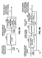
- FIG. 7A is block diagram illustrating the components of an Analog-to-Digital Converter (ADC) of the COder/DECoder (CODEC) of FIG. 6 that is constructed according to the present invention.
- the ADC 614 includes a modulator 702, e.g., sigma-delta, or delta-sigma modulator and a decimation filter 704.
- the modulator 702 receives an outbound analog audio signal (analog signal) from a coupled microphone 316, for example.
- the modulator 702 modulates the analog audio signal to produce a modulated signal at a modulator clock rate of 12 MHz.
- the decimation filter 704 receives the modulated signal at the modulator clock rate of 12 MHz, performs decimation and filtering operations on the modulated signal, and produces the outbound PCM audio data (digital data).
- the decimation filter produces the outbound PCM audio data as a 13 bit signal at 8 kHz.
- the modulator 702 includes a time dither clock reduction circuit 706. The operation of the time dither clock reduction circuit will be described in more detail with reference to FIG. 7B .
- FIG. 7B is block diagram illustrating in more detail the ADC 614 of FIG. 7A according to one embodiment of the present invention.
- the modulator 702 of the ADC 614 includes an analog delta sigma modulator 752 and the time dither clock reduction circuit 706.
- the analog sigma delta modulator 752 includes an integrator 764 and a quantizer 766.
- the quantizer 766 is a two level quantizer, e.g., produces the modulated signal at levels of logic 0 and logic 1.
- a three level quantizer or a more than three level quantizer may be employed.
- the time dither clock reduction circuit 706 includes time dither clock reduction logic 754 and an optional dithering factor generator 756.
- the integrator 764 receives as its inputs the analog signal and a feedback signal from the time dither clock reduction circuit 704.
- the quantizer 766 receives the output of the integrator 714 and produces the modulated signal at the modulator clock rate of 12 MHz.
- the time dither clock reduction circuit 704 receives the modulated signal from the quantizer 716 and produces the feedback signal to the integrator 764.
- the operation of the time dither clock reduction logic 754 will be described with particular reference to FIGs. 9 and 10 .
- the operation of the dithering factor generator 756 will be described with particular reference to FIG. 11 .
- the decimation filter 704 includes a 4 th order digital integrator 757, a decimator 758, a 4 th order digital differentiator 760, and a decimation filter 762.
- the modulated signal the modulator clock rate of 12 MHz produced by the quantizer 766 is also received by the 4 th order digital integrator 757 that produces a 34 bit output at 12 MHz.
- the 4 th order digital integrator 757 produces 34 bits at each of its stages.
- the decimator 758 receives the 34 bit output at 12 MHz from the 4 th order digital integrator 757 and produces a 34 bit output at 40 kHz.
- the 4 th order digital integrator 760 receives the 34 bit output at 40 kHz from the decimator 758 and produces an 18 bit output at 40 kHz.
- the decimation filter 762 receives the 18 bit output at 40 kHz from the 4 th order digital integrator 760 and produces the 13 bit signal at 8 kHz outbound PCM audio data (digital signal).
- FIG. 8A is block diagram illustrating the components of the DAC 612 of the CODEC 314 of FIG. 6 that is constructed according to the present invention.
- the DAC 612 includes an interpolation filter 802 and a modulator 804.
- the interpolation filter 802 receives inbound PCM audio data (digital data) that includes 13 bits per sample at a rate of 8 kHz.
- the interpolation filter 802 interpolates and filters the inbound PCM audio data to produce an interpolated and filtered digital signal (18 bit output at 12 MHz).
- the modulator 804 receives the 18 bit 12 MHz interpolated and filtered digital signal and modulates the interpolated and filtered digital signal to produce the modulated signal.
- the modulated signal, after filtering and smoothing is the analog signal that is presented to the speaker 318 illustrated in FIG. 6 .
- the modulator 802 includes a time dither clock reduction circuit 806.
- FIG. 8B is block diagram illustrating in more detail the modulator 804 of the DAC 612 of FIG. 8A according to one embodiment of the present invention.
- a noise shaping network 850 of the modulator 804 receives the 18 bit 12 MHz interpolation filter output and produces a 23 bit noise shaped digital signal.
- a quantizer 852 of the modulator 804 receives the 23 bit noise shaped digital signal, quantizes the 23 bit noise shaped digital signal (to two or more levels), and produces the modulated signal having two (or more) quantization levels at a modulator clock rate.
- the time dither clock reduction circuit 806 receives the modulated signal and performs clock reduction and time dithering operations upon the modulated signal to produce a time dithered/clock reduced modulated signal.
- the time dithered/clock reduced modulated signal is then filtered and smoothed to produce the analog signal.
- the time dithered/clock reduced modulated signal also serves as a feedback signal to the noise shaping network 850.
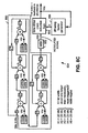
- FIG. 8C is a block diagram illustrating in more detail still the modulator 804 of the DAC 612 of FIG. 8A according to an embodiment of the present invention.
- the noise shaping network 850 includes a plurality of digital filtering components.
- the quantizer includes a Most Significant Bit(s) (MSB) circuit 852 that receives the output from the noise shaping network 852.
- the time dither clock reduction circuit 806 includes time dither clock reduction logic 854 and an optional dithering factor generator 856. The output of the MSB circuit 852 is received by the time dither clock reduction logic 854.
- the output of the time dither clock reduction logic 854 is the time dithered/clock reduced modulated signal that serves as the inbound analog audio signal (after optional filtering), as a feedback signal to control the state of all feedback switches of the noise shaping network 850, and as input to the dithering factor generator 856.
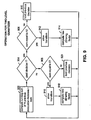
- FIG. 9 is a logic diagram illustrating operation of the time dither clock reduction circuit 706 of the ADC 614 of FIGs. 7A and 7B and of the time dither clock reduction circuit 806 of the DAC 612 of FIGS. 8A, 8B , and 8C according to the present invention for a two level quantizer.
- the time dither clock reduction circuit 706 of the ADC 614 operates to somewhat randomize the feedback signal provided to the modulator 702 of the ADC 614 while retaining the single bit resolution of the output of the modulator 702, i.e., the clock of the modulator 702 - 12 MHz.
- the time dither clock reduction circuit 806 of the DAC 612 operates to somewhat randomize the duration between transitions of the output of the DAC 612 and also to somewhat randomize the feedback provided to the noise shaping network 850 of the modulator 804 while maintaining a time resolution equal to the modulator clock rate.
- time dither clock reduction circuits 706 and 806 are inhibited from transitioning any faster than N modulator clock cycles, i.e., N cycles of the 12 MHz modulator clock rate of the embodiments described. Further, the time dither clock reduction circuits 706 and 806 introduce time dithering as well by using a running sum of the past N outputs of the respective modulator, e.g., V(k) of modulator 804. For a 2 level quantizer, which uses levels 1 and 0, the following algorithm may be employed:
- This algorithm is implemented in FIG. 9 by first computing the running sum of N previous modulator decisions (the "sum” at step 902). If the past decision of the time dither clock reduction circuit was a "1" (as determined at step 904), it is next determined whether the sum is equal to N (step 906). If the sum is not equal to N, the previous output of the time dither clock reduction circuit V(k) is held (step 910). If the sum is equal to N, the output of the time dither clock reduction circuit V(k) is allowed to transition (step 912). Thus, if the past N modulated signals were 1, and the current modulated signal is 0, the time dither clock reduction circuit V(k) is allowed to transition from a 1 to a 0.
- a new dithering factor (value of N) is optionally determined (step 914). The manner in which the dithering factor N is determined will be described with particular reference to FIG. 11 .
- step 908 it is next determined whether the sum is equal to 0 (step 908). If the sum is not equal to 0, the previous output of the time dither clock reduction circuit V(k) is held (step 920). If the sum is equal to 0, the output of the time dither clock reduction circuit V(k) is allowed to transition (step 916). Thus, if modulated signal is a 1 for the current modulator clock cycle, the output of the time dither clock reduction circuit V(k) will transition from a 0 to a 1.
- a new dithering factor (value of N) is optionally determined (step 914). From each of steps 910, 914, 918, and 920, operation returns to step 902 where the steps of FIG. 9 are repeated for the next clock cycle.
- single modulator clock cycle resolution is maintained at the output of the time dither clock reduction circuits 706 or 806.
- Single modulator clock cycle resolution at the output of the DAC 612 results in a more accurate production of the analog audio signal.
- Single modulator clock cycle resolution at the time dither clock reduction circuit 706 of the modulator 702 of the ADC 614 causes the modulator to better track the analog input signal. Further, by limiting the transitions of the time dither clock reduction circuit 706 or 806, power consumption of the ADC 614 and DAC 612 are reduced.
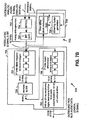
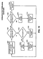
- FIG. 10 is a logic diagram illustrating operation of the time dither clock reduction circuit of the ADC of FIGs. 7A and 7B and of the time dither clock reduction circuits of the DAC of FIGs. 8A, 8B , and 8C according to the present invention for a three level quantizer.
- the 3 level modulator output and feedback signal feedback V(k) is inhibited from transitioning any faster than N clocks.
- the 3 level quantizer modulator uses levels 1, 0 and -1.
- This algorithm is implemented in FIG. 10 by first computing the running sum of N previous modulator decisions (the "sum” at step 1002). If the absolute value of the past decision of the modulator was a "1" (as determined at step 1004), it is next determined whether the absolute value of the sum is equal to N (step 1006). If the absolute value of the sum is not equal to N, the previous output of the time dither clock reduction circuit V(k) is held (step 1010). If the sum is equal to N, the output of the time dither clock reduction circuit V(k) is allowed to transition with the modulated signal (step 1012).
- a new dithering factor (value of N) is optionally determined (step 1014). The manner in which the dithering factor N is determined will be described with particular reference to FIG. 11 .
- step 1008 it is next determined whether the sum is equal to 0 (step 1008). If the sum is not equal to 0, the previous output of the time dither clock reduction circuit V(k) is held (step 1020). If the sum is equal to 0, the output of the time dither clock reduction circuit V(k) is allowed to transition with the modulated signal (step 1016). Further, if the output of the modulator is allowed to transition at step 1016, a new dithering factor (value of N) is optionally determined (step 1014). From each of steps 1010, 1014, 1018, and 1020, operation returns to step 1002 where the steps of FIG. 10 are repeated for the next clock cycle.
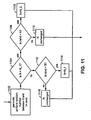
- FIG. 11 is a logic diagram illustrating operation of the dithering factor generator of the time dither clock reduction circuits of the ADC of FIGs. 7A and 7B and of the time dither clock reduction circuits of the DAC of FIGs. 8A, 8B , and 8C .
- the purpose of adjusting the dithering factor N is to allow time dither to be added to the modulator transitions. This advantage is not possible using amplitude dither. Time dither can be added in precisely controlled amounts using the principles of the present invention.
- the clock reduction circuit in determining a dithering factor, is allowed to randomly switch between two dithering factors N_1 and N_2. By changing the values of the dithering factor N at some modulator output transitions, a satisfactory degree of randomness is achieved. In other embodiments more than two dithering factors may be used. As was explained in the operations of FIG. 9 and FIG. 10 , the dithering factor is adjusted only after the time dither clock reduction logic 754 or 854 has allowed the modulator output to transition (at step 914 or 918 of FIG. 9 and at step 1014 or 1018 of FIG. 10 ).
- N is not equal to N_1 (as determined at step 1104), it is next determined whether rand is greater than B (step 1112).
- the value of B is chosen as .9 in the embodiment of FIG. 11 . If rand is greater than B, the dithering factor N is set to N_1 for the next transition cycle (step 1114). However, if rand is not greater than B, the dithering factor N remains unchanged for the subsequent transition cycle (step 1116). From each of steps 1108, 1110, 1114, and 1116, operation continues to step 902 of FIG. 9 or 1002 of FIG. 10 .
- FIG. 12 is a graph illustrating the delta sigma response of a prior art ADC during quiet periods that includes a plurality of idle tones. As is illustrated, the prior art ADC exhibits significant tonal noise in both the audio range and in the EMI range.
- FIG. 13 is a graph illustrating the delta sigma response of an ADC constructed according to the present invention that illustrates the absence of idle tones during quiet periods.
- the ADC of the present invention has significantly reduced tonal noise in both the audio range and in the EMI range as compared to the ADC whose response is illustrated in FIG. 12 .
- FIG. 14 is a graph illustrating the frequency response of a prior art ADC within the audio band that includes a plurality of idle tones produced when the ADC is stimulated by a low level DC input. As is illustrated, significant tonal noise exists.
- FIG. 15 is a graph illustrating the frequency response of an ADC constructed according to the present invention within the audio band when the ADC is stimulated by a low level DC input. As contrasted to the ADC behavior illustrated in FIG. 14 , tonal noise is significantly reduced in the audio band.
Landscapes
- Engineering & Computer Science (AREA)
- Theoretical Computer Science (AREA)
- Computer Networks & Wireless Communication (AREA)
- Signal Processing (AREA)
- Transceivers (AREA)
Claims (20)
- Integrierter Sende/Empfangs-Schaltkreis (300) für ein WLAN (Wireless Local Area Network; drahtloses lokales Netzwerk), der Sprachkommunikationen in einem WLAN mit wenigstens einer WLAN-Vorrichtung verwaltet, wobei der integrierte WLAN-Sende/Empfangs-Schaltkreis (300) Folgendes umfasst:eine WLAN-Schnittstelle, die drahtlos mit der wenigstens einen WLAN-Vorrichtung kommuniziert, um ankommende paketierte Audiodaten von der wenigstens einen WLAN-Vorrichtung zu empfangen und abgehende paketierte Audiodaten zu der wenigstens einen WLAN-Vorrichtung zu senden;einen Codeumsetzer bzw. Transcoder (602), der betriebsbereit mit der WLAN-Schnittstelle gekoppelt ist, wobei der Codeumsetzer (602) die ankommenden paketierten Audiodaten empfängt und die ankommenden paketierten Audiodaten in ankommende pulscodemodulierte/PCM (pulse code modulated)-WLAN-Audiodaten umwandelt, und wobei der Codeumsetzer (602) abgehende PCM-WLAN-Audiodaten empfängt unddie abgehenden PCM-WLAN-Audiodaten in die abgehenden paketierten Audiodaten umwandelt; undeinen Audio-Codierer/Decodierer (314), der betriebsbereit mit dem Codeumsetzer (602) gekoppelt ist, wobei der Codierer/Decodierer (314) einen Digital-Analog-Umsetzer (DAC; digital-to-analog converter) (612) umfasst, der die abgehenden PCM-WLAN-Audiodaten empfängt und der ein analoges Audiosignal erzeugt, wobei der DAC (612) Folgendes umfasst:einen Interpolationsfilter (802), der die abgehenden PCM-WLAN-Audiodaten empfängt und der die abgehenden PCM-WLAN-Audiodaten interpoliert und filtert, um ein interpoliertes und gefiltertes digitales Signal zu erzeugen;einen Modulator (804), der das interpolierte und gefilterte digitale Signal und ein Rückkopplungssignal empfängt, wobei der Modulator (804) das interpolierte und gefilterte digitale Signal auf der Basis des Rückkopplungssignals moduliert, um ein moduliertes Signal bei einer Modulatortaktfrequenz zu erzeugen; undeine Zeit-Dither-/Taktreduktions-Schaltung (806), die das modulierte Signal empfängt, wobei die Zeit-Dither-/Taktreduktions-Schaltung (806) sowohl eine Taktreduktion als auch ein Zeit-Dithering an das modulierte Signal anlegt, um ein einem Zeit-Dithering unterzogenes/taktreduziertes moduliertes Signal zu erzeugen, und wobei das einem Zeit-Dithering unterzogene/taktreduzierte modulierte Signal als das analoge Audiosignal dient und auch als das Rückkopplungssignal dient.
- Integrierter WLAN-Sende/Empfangs-Schaltkreis (300) nach Anspruch 1, wobei:in jedem Modulatortaktzyklus die Zeit-Dithering-/Taktreduktions-Schaltung modulierte Signale im Hinblick auf einen Dithering-Faktor, N, vorhergehende Modulatortaktzyklen und ein moduliertes Signal im Hinblick auf einen aktuellen Modulatortaktzyklus überprüft; und dann,wenn wenigstens eine Bedingung für die N vorhergehenden Modulatortaktzyklen erfüllt ist, die Zeit-Dithering-/Taktreduktions-Schaltung das einem Zeit-Dithering unterzogene/taktreduzierte modulierte Signal mit dem modulierten Signal wechselt.
- Integrierter WLAN-Sende/Empfangs-Schaltkreis (300) nach Anspruch 1, wobei dann, wenn das vorherige, einem Zeit-Dithering unterzogene/taktreduzierte modulierte Signal Eins ist, eine Summe der modulierten Signale für die N vorhergehenden Modulatortakte gleich N ist und das modulierte Signal für den aktuellen Modulatortakt Null ist, die Zeit-Dithering-/Taktreduktions-Schaltung das einem Zeit-Dithering unterzogene/taktreduzierte modulierte Signal von Eins auf Null wechselt.
- Integrierter WLAN-Sende/Empfangs-Schaltkreis (300) nach Anspruch 1, wobei dann, wenn das vorherige, einem Zeit-Dithering unterzogene/taktreduzierte modulierte Signal Eins ist, eine Summe der modulierten Signale für die N vorhergehenden Modulatortakte gleich N ist und das modulierte Signal für den aktuellen Modulatortakt Eins ist, die Zeit-Dithering-/Taktreduktions-Schaltung das einem Zeit-Dithering unterzogene/taktreduzierte modulierte Signal auf Eins hält.
- Integrierter WLAN-Sende/Empfangs-Schaltkreis (300) nach Anspruch 1, wobei dann, wenn das vorherige, einem Zeit-Dithering unterzogene/taktreduzierte modulierte Signal Null ist, eine Summe der modulierten Signale für die N vorhergehenden Modulatortakte gleich Null ist und das modulierte Signal für den aktuellen Modulatortakt Eins ist, die Zeit-Dithering-/Taktreduktions-Schaltung das einem Zeit-Dithering unterzogene/taktreduzierte modulierte Signal von Null auf Eins wechselt.
- Integrierter WLAN-Sende/Empfangs-Schaltkreis (300) nach Anspruch 1, wobei dann, wenn das vorherige, einem Zeit-Dithering unterzogene/taktreduzierte modulierte Signal Null ist, eine Summe der modulierten Signale für die N vorhergehenden Modulatortakte gleich Null ist und das modulierte Signal für den aktuellen Modulatortakt Null ist, die Zeit-Dithering-/Taktreduktions-Schaltung das einem Zeit-Dithering unterzogene/taktreduzierte modulierte Signal auf Null hält.
- Integrierter WLAN-Sende/Empfangs-Schaltkreis (300) nach Anspruch 1, wobei dann, nachdem es der Zeit-Dithering-/Taktreduktions-Schaltung erlaubt ist, das einem Zeit-Dithering unterzogene/taktreduzierte modulierte Signal mit dem modulierten Signal zu wechseln, ein neuer Dithering-Faktor, N, ausgewählt wird.
- Integrierter WLAN-Sende/Empfangs-Schaltkreis (300) nach Anspruch 7, wobei der neue Dithering-Faktor bestimmt wird durch das:Erzeugen einer Zufallszahl; undder neue Dithering-Faktor auf einem Vergleich der Zufallszahl mit wenigstens einer Bedingung basiert.
- Integrierter WLAN-Sende/Empfangs-Schaltkreis (300) nach Anspruch 1, wobei der Modulator (804) Folgendes umfasst:ein Rauschformungs-/Noise Shaping-Netzwerk, das das interpolierte und gefilterte digitale Signal und ein Rückkopplungssignal empfängt, wobei das Rauschformungsnetzwerk das interpolierte und gefilterte digitale Signal einer Rauschformung unterzieht, also 'rauschformt', um ein rauschgeformtes digitales Signal zu bilden; undeinen Quantisierer, der das rauschgeformte digitale Signal empfängt und das rauschgeformte digitale Signal quantisiert, um das modulierte Signal bei der Modulatortaktfrequenz zu erzeugen.
- Integrierter WLAN-Sende/Empfangs-Schaltkreis (300) nach Anspruch 1, wobei:das modulierte Signal wenigstens drei Pegel umfasst, die -1, 0 und 1 umfassen;bei jedem Modulatortaktzyklus die Zeit-Dithering-/Taktreduktions-Schaltung modulierte Signale im Hinblick auf einen Dithering-Faktor, N,vorhergehende Modulatortaktzyklen und ein moduliertes Signal im Hinblick auf einen aktuellen Modulatortaktzyklus überprüft; und wobei dann,wenn wenigstens eine Bedingung für die N vorhergehenden Modulatortaktzyklen erfüllt ist, die Zeit-Dithering-/Taktreduktions-Schaltung das einem Zeit-Dithering unterzogene/taktreduzierte modulierte Signal mit dem modulierten Signal wechselt.
- Integrierter WLAN-Sende/Empfangs-Schaltkreis (300) nach Anspruch 1, wobei das Rauschformungsnetzwerk eine Vielzahl von Rauschformungsstufen umfasst, die auf der Basis des Rückkopplungssignals gewechselt werden.
- Integrierter WLAN-Sende/Empfangs-Schaltkreis (300) nach Anspruch 1, wobei die Zeit-Dither-/Taktreduktions-Schaltung (806) eine Zeit-Dither-/Taktreduktions-Logik und einen Dithering-Faktor-Generator umfasst.
- Verfahren zum Umwandeln eines digitalen Signals in ein analoges Signal zur Verwendung in einem Digital-Analog-Umsetzer DAC (612), der in einem integrierten Sende/Empfangs-Schaltkreis (300) für ein WLAN (Wireless Local Area Network; drahtloses lokales Netzwerk) enthalten ist, der Sprachkommunikationen in einem WLAN mit wenigstens einer WLAN-Vorrichtung verwaltet, wobei das Verfahren Folgendes umfasst:Empfangen der digitalen Daten, Interpolieren der digitalen Daten und Filtern der digitalen Daten, um ein interpoliertes und gefiltertes digitales Signal zu erzeugen;Modulieren des interpolierten und gefilterten digitalen Signals auf der Basis eines Rückkopplungssignals, um ein moduliertes Signal bei einer Modulatortaktfrequenz zu erzeugen; undAnlegen sowohl der Taktreduktion als auch des Zeit-Dithering an das modulierte Signal, um ein einem Zeit-Dithering unterzogenes/taktreduziertes moduliertes Signal zu erzeugen, wobei das einem Zeit-Dithering unterzogene/ taktreduzierte modulierte Signal als das analoge Signal dient und auch als das Rückkopplungssignal dient.
- Verfahren nach Anspruch 13, das des Weiteren Folgendes umfasst:bei jedem Modulatortaktzyklus das Überprüfen von modulierten Signalen im Hinblick auf einen Dithering-Faktor, N, vorhergehende Modulatortaktzyklen und das modulierte Signal im Hinblick auf einen aktuellen Modulatortaktzyklus; und,wenn wenigstens eine Bedingung für die N vorhergehenden Modulatortaktzyklen erfüllt ist, das Wechseln bzw. Vollziehen eines Übergangs des einem Zeit-Dithering unterzogenen/taktreduzierten modulierten Signals mit dem modulierten Signal.
- Verfahren nach Anspruch 13, das des Weiteren das Wechseln bzw. Übergehen des einem Zeit-Dithering unterzogenen/taktreduzierten modulierten Signals von Eins auf Null umfasst, wenn:das vorherige, einem Zeit-Dithering unterzogene/taktreduzierte modulierte Signal Eins ist;eine Summe der modulierten Signale für die N vorhergehenden Modulatortakte gleich N ist; unddas modulierte Signal für den aktuellen Modulatortakt Null ist.
- Verfahren nach Anspruch 13, das des Weiteren das Halten des einem Zeit-Dithering unterzogenen/taktreduzierten modulierten Signals auf Eins umfasst, wenn:das vorherige, einem Zeit-Dithering unterzogene/taktreduzierte modulierte Signal Eins ist;eine Summe der modulierten Signale für die N vorhergehenden Modulatortakte gleich N ist; unddas modulierte Signal für den aktuellen Modulatortakt Eins ist
- Verfahren nach Anspruch 13, das des Weiteren das Wechseln bzw. Übergehen des einem Zeit-Dithering unterzogenen/taktreduzierten modulierten Signals von Null auf Eins umfasst, wenn:das vorherige, einem Zeit-Dithering unterzogene/taktreduzierte modulierte Signal Null ist;eine Summe der modulierten Signale für die N vorhergehenden Modulatortakte gleich Null ist; unddas modulierte Signal für den aktuellen Modulatortakt Eins ist.
- Verfahren nach Anspruch 13, das des Weiteren das Halten des einem Zeit-Dithering unterzogenen/taktreduzierten modulierten Signals auf Null umfasst, wenn:das vorherige, einem Zeit-Dithering unterzogene/taktreduzierte modulierte Signal Null ist;eine Summe der modulierten Signale für die N vorhergehenden Modulatortakte gleich Null ist; unddas modulierte Signal für den aktuellen Modulatortakt Null ist
- Verfahren nach Anspruch 13, das des Weiteren das Auswählen eines neuen Dithering-Faktors, N, umfasst, wenn das einem Zeit-Dithering unterzogene/taktreduzierte modulierte Signal mit dem modulierten Signal wechselt bzw. einen Übergang vollzieht.
- Verfahren nach Anspruch 13, das des Weiteren das Auswählen des neuen Dithering-Faktors umfasst durch das:Erzeugen einer Zufallszahl; undBestimmen des neuen Dithering-Faktors auf der Basis eines Vergleichs der Zufallszahl mit wenigstens einer Bedingung.
Applications Claiming Priority (6)
| Application Number | Priority Date | Filing Date | Title |
|---|---|---|---|
| US35632302P | 2002-02-12 | 2002-02-12 | |
| US356323P | 2002-02-12 | ||
| US40284202P | 2002-08-12 | 2002-08-12 | |
| US402842P | 2002-08-12 | ||
| US230738 | 2002-08-29 | ||
| US10/230,738 US7031401B2 (en) | 2002-02-12 | 2002-08-29 | Digital to analog converter with time dithering to remove audio tones |
Publications (3)
| Publication Number | Publication Date |
|---|---|
| EP1335532A2 EP1335532A2 (de) | 2003-08-13 |
| EP1335532A3 EP1335532A3 (de) | 2006-06-07 |
| EP1335532B1 true EP1335532B1 (de) | 2011-05-11 |
Family
ID=27617520
Family Applications (1)
| Application Number | Title | Priority Date | Filing Date |
|---|---|---|---|
| EP03002972A Expired - Lifetime EP1335532B1 (de) | 2002-02-12 | 2003-02-11 | Digital-/Analogkonverter mit Zeit-Dithering zum Ausblenden von Audiotönen |
Country Status (2)
| Country | Link |
|---|---|
| US (1) | US7031401B2 (de) |
| EP (1) | EP1335532B1 (de) |
Families Citing this family (12)
| Publication number | Priority date | Publication date | Assignee | Title |
|---|---|---|---|---|
| US7133926B2 (en) * | 2001-09-28 | 2006-11-07 | Hewlett-Packard Development Company, L.P. | Broadcast compressed firmware flashing |
| KR100901034B1 (ko) * | 2004-04-01 | 2009-06-04 | 신토고교 가부시키가이샤 | 감압 주형조형의 주탕 방법, 장치 및 주물 |
| US7627700B2 (en) * | 2007-06-05 | 2009-12-01 | Texas Instruments Incorporated | Expanded memory for communications controller |
| US8132037B2 (en) * | 2008-06-06 | 2012-03-06 | Roche Diagnostics International Ag | Apparatus and method for processing wirelessly communicated data and clock information within an electronic device |
| US8117481B2 (en) * | 2008-06-06 | 2012-02-14 | Roche Diagnostics International Ag | Apparatus and method for processing wirelessly communicated information within an electronic device |
| US8030959B2 (en) * | 2008-06-12 | 2011-10-04 | Texas Instruments Incorporated | Device-under-test power management |
| CN104618666B (zh) * | 2013-11-05 | 2018-04-10 | 南宁富桂精密工业有限公司 | 音频信号控制电路 |
| KR102251813B1 (ko) * | 2015-04-07 | 2021-05-13 | 삼성전자주식회사 | 메모리 시스템 및 메모리 시스템의 동작 방법 |
| CN106788569A (zh) * | 2017-02-27 | 2017-05-31 | 广东顺德中山大学卡内基梅隆大学国际联合研究院 | 一种无线局域网射频收发机电路芯片 |
| EP3471271A1 (de) * | 2017-10-16 | 2019-04-17 | Acoustical Beauty | Verbesserte konvolutionen von digitalen signalen mit verwendung einer bitanforderungsoptimierung eines digitalen zielsignals |
| US10319360B1 (en) * | 2018-03-06 | 2019-06-11 | GM Global Technology Operations LLC | Active masking of tonal noise using motor-based acoustic generator to improve sound quality |
| GB2579858B (en) * | 2018-12-18 | 2021-07-14 | Mqa Ltd | Discrete dither |
Family Cites Families (7)
| Publication number | Priority date | Publication date | Assignee | Title |
|---|---|---|---|---|
| US5648777A (en) | 1993-12-16 | 1997-07-15 | Lucent Technologies Inc. | Data converter with FIFO |
| US6580700B1 (en) * | 1995-10-27 | 2003-06-17 | Symbol Technologies, Inc. | Data rate algorithms for use in wireless local area networks |
| AU3195399A (en) | 1998-03-26 | 1999-10-18 | Ess Technology, Inc. | Tone modulation in delta-sigma dac using square wave dither |
| DE60030086T2 (de) * | 2000-01-20 | 2007-01-04 | Lucent Technologies Inc. | Interoperabilität von Bluetooth und IEEE 802.11 |
| EP1146691A1 (de) * | 2000-04-10 | 2001-10-17 | Siemens Information and Communication Networks S.p.A. | Verbindung von Funkzellen mit einer Funknetzsteuerung durch kupferkabelpaaren mit Hilfe der DMT-Technologie |
| CN1147177C (zh) * | 2000-09-26 | 2004-04-21 | 华为技术有限公司 | 一种提高宽带多载波基站载波输出功率的方法及其装置 |
| US6661360B2 (en) * | 2002-02-12 | 2003-12-09 | Broadcom Corporation | Analog to digital converter that services voice communications |
-
2002
- 2002-08-29 US US10/230,738 patent/US7031401B2/en not_active Expired - Lifetime
-
2003
- 2003-02-11 EP EP03002972A patent/EP1335532B1/de not_active Expired - Lifetime
Also Published As
| Publication number | Publication date |
|---|---|
| EP1335532A3 (de) | 2006-06-07 |
| US20030152161A1 (en) | 2003-08-14 |
| US7031401B2 (en) | 2006-04-18 |
| EP1335532A2 (de) | 2003-08-13 |
Similar Documents
| Publication | Publication Date | Title |
|---|---|---|
| EP1335543B1 (de) | Verbesserter Analog-/Digitalkonverter zur Durchführung von Sprachkommunikation | |
| US7953057B2 (en) | Packetized audio data operations in a wireless local area network device | |
| US8207880B2 (en) | Wireless local area network device supporting enhanced call functions | |
| US7944907B2 (en) | Temporal alignment of codec data with wireless local area network RF slots | |
| EP2082556B1 (de) | Verfahren und vorrichtung zur wartschlangensteuerung für bidirektionale dualmodus-audiokommunikation | |
| EP1335532B1 (de) | Digital-/Analogkonverter mit Zeit-Dithering zum Ausblenden von Audiotönen | |
| US9031604B2 (en) | Method and apparatus for enabling simultaneous VoWLAN and Bluetooth audio in small form factor handheld devices | |
| US20020077072A1 (en) | Radio transmitter and receiver | |
| US6518902B2 (en) | PC card and WLAN system having high speed, high resolution, digital-to analog converter with off-line sigma delta conversion and storage | |
| CN101480072B (zh) | 控制方法、控制设备、通信设备、计算机程序、计算机程序分发介质和数据处理方法 | |
| US6489908B2 (en) | Wireless local loop terminal and system having high speed, high resolution, digital-to-analog converter with off-line sigma-delta conversion and storage |
Legal Events
| Date | Code | Title | Description |
|---|---|---|---|
| PUAI | Public reference made under article 153(3) epc to a published international application that has entered the european phase |
Free format text: ORIGINAL CODE: 0009012 |
|
| AK | Designated contracting states |
Designated state(s): AT BE BG CH CY CZ DE DK EE ES FI FR GB GR HU IE IT LI LU MC NL PT SE SI SK TR |
|
| AX | Request for extension of the european patent |
Extension state: AL LT LV MK RO |
|
| PUAL | Search report despatched |
Free format text: ORIGINAL CODE: 0009013 |
|
| AK | Designated contracting states |
Kind code of ref document: A3 Designated state(s): AT BE BG CH CY CZ DE DK EE ES FI FR GB GR HU IE IT LI LU MC NL PT SE SI SK TR |
|
| AX | Request for extension of the european patent |
Extension state: AL LT LV MK RO |
|
| 17P | Request for examination filed |
Effective date: 20061207 |
|
| AKX | Designation fees paid |
Designated state(s): DE FR GB |
|
| RAP1 | Party data changed (applicant data changed or rights of an application transferred) |
Owner name: BROADCOM CORPORATION |
|
| 17Q | First examination report despatched |
Effective date: 20100303 |
|
| GRAP | Despatch of communication of intention to grant a patent |
Free format text: ORIGINAL CODE: EPIDOSNIGR1 |
|
| RIC1 | Information provided on ipc code assigned before grant |
Ipc: H04W 84/12 20090101ALN20101013BHEP Ipc: H04W 4/18 20090101AFI20101013BHEP |
|
| RIC1 | Information provided on ipc code assigned before grant |
Ipc: H03M 3/02 20060101AFI20101025BHEP Ipc: H04W 84/12 20090101ALN20101025BHEP Ipc: H03M 7/00 20060101ALN20101025BHEP |
|
| GRAS | Grant fee paid |
Free format text: ORIGINAL CODE: EPIDOSNIGR3 |
|
| GRAA | (expected) grant |
Free format text: ORIGINAL CODE: 0009210 |
|
| AK | Designated contracting states |
Kind code of ref document: B1 Designated state(s): DE FR GB |
|
| REG | Reference to a national code |
Ref country code: GB Ref legal event code: FG4D |
|
| REG | Reference to a national code |
Ref country code: DE Ref legal event code: R096 Ref document number: 60337044 Country of ref document: DE Effective date: 20110622 |
|
| PLBE | No opposition filed within time limit |
Free format text: ORIGINAL CODE: 0009261 |
|
| STAA | Information on the status of an ep patent application or granted ep patent |
Free format text: STATUS: NO OPPOSITION FILED WITHIN TIME LIMIT |
|
| 26N | No opposition filed |
Effective date: 20120214 |
|
| REG | Reference to a national code |
Ref country code: DE Ref legal event code: R097 Ref document number: 60337044 Country of ref document: DE Effective date: 20120214 |
|
| REG | Reference to a national code |
Ref country code: FR Ref legal event code: ST Effective date: 20121031 |
|
| PG25 | Lapsed in a contracting state [announced via postgrant information from national office to epo] |
Ref country code: FR Free format text: LAPSE BECAUSE OF NON-PAYMENT OF DUE FEES Effective date: 20120229 |
|
| PGFP | Annual fee paid to national office [announced via postgrant information from national office to epo] |
Ref country code: DE Payment date: 20130228 Year of fee payment: 11 |
|
| PGFP | Annual fee paid to national office [announced via postgrant information from national office to epo] |
Ref country code: GB Payment date: 20140220 Year of fee payment: 12 |
|
| REG | Reference to a national code |
Ref country code: DE Ref legal event code: R119 Ref document number: 60337044 Country of ref document: DE |
|
| REG | Reference to a national code |
Ref country code: DE Ref legal event code: R119 Ref document number: 60337044 Country of ref document: DE Effective date: 20140902 |
|
| PG25 | Lapsed in a contracting state [announced via postgrant information from national office to epo] |
Ref country code: DE Free format text: LAPSE BECAUSE OF NON-PAYMENT OF DUE FEES Effective date: 20140902 |
|
| GBPC | Gb: european patent ceased through non-payment of renewal fee |
Effective date: 20150211 |
|
| PG25 | Lapsed in a contracting state [announced via postgrant information from national office to epo] |
Ref country code: GB Free format text: LAPSE BECAUSE OF NON-PAYMENT OF DUE FEES Effective date: 20150211 |