EP1338954B1 - Additionsschaltung zum Akkumulieren von Binärzahlen in redundanter Darstellung - Google Patents
Additionsschaltung zum Akkumulieren von Binärzahlen in redundanter Darstellung Download PDFInfo
- Publication number
- EP1338954B1 EP1338954B1 EP03004149A EP03004149A EP1338954B1 EP 1338954 B1 EP1338954 B1 EP 1338954B1 EP 03004149 A EP03004149 A EP 03004149A EP 03004149 A EP03004149 A EP 03004149A EP 1338954 B1 EP1338954 B1 EP 1338954B1
- Authority
- EP
- European Patent Office
- Prior art keywords
- field
- sum
- carry
- bits
- save
- Prior art date
- Legal status (The legal status is an assumption and is not a legal conclusion. Google has not performed a legal analysis and makes no representation as to the accuracy of the status listed.)
- Expired - Lifetime
Links
Images



Classifications
-
- G—PHYSICS
- G06—COMPUTING OR CALCULATING; COUNTING
- G06F—ELECTRIC DIGITAL DATA PROCESSING
- G06F7/00—Methods or arrangements for processing data by operating upon the order or content of the data handled
- G06F7/60—Methods or arrangements for performing computations using a digital non-denominational number representation, i.e. number representation without radix; Computing devices using combinations of denominational and non-denominational quantity representations, e.g. using difunction pulse trains, STEELE computers, phase computers
- G06F7/607—Methods or arrangements for performing computations using a digital non-denominational number representation, i.e. number representation without radix; Computing devices using combinations of denominational and non-denominational quantity representations, e.g. using difunction pulse trains, STEELE computers, phase computers number-of-ones counters, i.e. devices for counting the number of input lines set to ONE among a plurality of input lines, also called bit counters or parallel counters
-
- G—PHYSICS
- G06—COMPUTING OR CALCULATING; COUNTING
- G06F—ELECTRIC DIGITAL DATA PROCESSING
- G06F2207/00—Indexing scheme relating to methods or arrangements for processing data by operating upon the order or content of the data handled
- G06F2207/38—Indexing scheme relating to groups G06F7/38 - G06F7/575
- G06F2207/3804—Details
- G06F2207/3808—Details concerning the type of numbers or the way they are handled
- G06F2207/3828—Multigauge devices, i.e. capable of handling packed numbers without unpacking them
-
- G—PHYSICS
- G06—COMPUTING OR CALCULATING; COUNTING
- G06F—ELECTRIC DIGITAL DATA PROCESSING
- G06F7/00—Methods or arrangements for processing data by operating upon the order or content of the data handled
- G06F7/38—Methods or arrangements for performing computations using exclusively denominational number representation, e.g. using binary, ternary, decimal representation
- G06F7/48—Methods or arrangements for performing computations using exclusively denominational number representation, e.g. using binary, ternary, decimal representation using non-contact-making devices, e.g. tube, solid state device; using unspecified devices
- G06F7/52—Multiplying; Dividing
- G06F7/523—Multiplying only
- G06F7/53—Multiplying only in parallel-parallel fashion, i.e. both operands being entered in parallel
- G06F7/5318—Multiplying only in parallel-parallel fashion, i.e. both operands being entered in parallel with column wise addition of partial products, e.g. using Wallace tree, Dadda counters
-
- G—PHYSICS
- G06—COMPUTING OR CALCULATING; COUNTING
- G06F—ELECTRIC DIGITAL DATA PROCESSING
- G06F7/00—Methods or arrangements for processing data by operating upon the order or content of the data handled
- G06F7/38—Methods or arrangements for performing computations using exclusively denominational number representation, e.g. using binary, ternary, decimal representation
- G06F7/48—Methods or arrangements for performing computations using exclusively denominational number representation, e.g. using binary, ternary, decimal representation using non-contact-making devices, e.g. tube, solid state device; using unspecified devices
- G06F7/544—Methods or arrangements for performing computations using exclusively denominational number representation, e.g. using binary, ternary, decimal representation using non-contact-making devices, e.g. tube, solid state device; using unspecified devices for evaluating functions by calculation
- G06F7/5443—Sum of products
Definitions
- the present invention relates to multiplier accumulator circuits (hereinafter referred to as "MACs"), and more particularly, to MACs that provide optimized performance for specific redundant binary data formats.
- MACs multiplier accumulator circuits
- a MAC is a circuit structure that may be utilized by a microprocessor or other data processing device to sequentially multiply a string of binary numbers, and accumulate the resulting products.
- the microprocessor can usually perform such a multiply-accumulate operation with its own internal resources, it typically takes a relatively large number of instruction cycles to do so.
- the processor can multiply and accumulate the results at a much higher rate, depending upon the architecture of the MAC.
- FIG. 1 illustrates one specific data processing architecture that can not be optimally handled by a general purpose MAC.
- FIG. 1 represents four lanes of a single instruction, multiple data (SIMD) processing architecture.
- SIMD single instruction, multiple data
- a multiplier 12 multiplies two 16-bit numbers.
- the multiplier 12 represents the multiplication product with a 40-bit number (32 bits for the maximum product, plus 8 extra bits for subsequent summation overflow).
- An accumulator 14 receives the four 40-bit products and produces a single 40-bit number 16 that represents the sum of the four 40-bit products. In other words, the accumulator 14 adds across the four SIMD lanes to produce a single sum as an output. Although not shown, the output of the accumulator 14 may propagate to a registered accumulator that adds the current output of the accumulator 14 to the registered result of the previous N samples of the accumulator 14, and then registers the result for the next iteration.
- the 40-bit numbers in this example are represented in radix-16 format, such that a carry-save bit for every four operand bits provides arithmetic redundancy (the data fields are shown to be 40+c wide, where the "c" represents the carry-save bits that accompany the 40 operand bits).
- the increase in processing efficiency comes at the cost of additional storage requirements due to the extra carry-save bits.
- the carry-save bits are sparsely distributed across the full field of 40 operand bits, so that the carry-save word field is similar in size to the 40-bit operand.
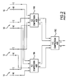
- a prior art technique of adding the four 40-bit numbers is shown in block diagram form in FIG. 2 .
- a first 4:2 compression adding block 18A receives the four 40-bit operands, and a second 4:2 compression adder block 18B receives the four sets of carry-save bits.
- Each of the first and second 4:2 blocks 18A and 18B produces a sum field and a carry field.
- a third 4:2 compression adder block 18C receives the two sum fields and the two carry fields from the first and second 4:2 blocks 18A and 18B.
- FIG. 3 shows a 4:2 compression adder block is simply a cascade of two full adders, which are 3:2 compression adding blocks.
- the delay through a 4:2 compression adding block is therefore equal to twice the delay through a full adder, and the delay through the adder tree configuration shown in FIG. 2 is equal to four times the delay through a full adder. Since a pair of numbers encounters this delay for each iteration of the MAC, any reduction in the delay would be significant when compounded by a large number of iterations through the adder tree.
- US 2001/0037442 refers to an application specific signal processor which comprises, inter alia, a plurality of signal processing units.
- One of the signal processing units comprises two 4-to-2 compressors having their outputs coupled into the inputs of a third 4-to-2 compressor.
- the outputs of the third 4-to-2 compressor are connected with inputs of a 3-to-2 compressor having its outputs connected to a full adder.
- an addition circuit as defined by independent claim 1 and a method of producing a sum of four redundant binary numbers as defined by independent claim 7.
- FIG. 1 illustrates four lanes of a single instruction, multiple data (SIMD) processing architecture
- FIG. 2 shows a prior art method of adding the four 40-bit numbers
- FIG. 3 shows a more detailed view of the 4:2 compression adding blocks of FIG. 2 ;
- FIG. 4 shows a block diagram view of one preferred embodiment of an accumulator according to the present invention
- FIG. 5 illustrates the numerical operation of the 3:2 compression adder of FIG. 4 ;
- FIG. 6 illustrates the numerical operation of the 4:2 compression adder of FIG. 4 ;
- FIG. 7 illustrates the numerical operation of the 4:3 compression adder of FIG. 4 ;
- FIG. 8 provides a more detailed illustration of the 4:3 compression adder of FIG. 4 ;
- FIG. 9 shows a carry-save bit for every four operand bits for a value in radix-16 format
- FIG. 10A shows graphically how the 4:2 compression adder of FIG. 4 produces a sum word and a carry-save word from the four operand input words
- FIG. 10B shows graphically how the 4:3 compression adder of FIG. 4 produces a sum word from the four sparse carry-save input words
- FIG. 10C shows graphically how the 3:2 compression adder of FIG. 4 produces a sum word and a carry-save word from the outputs of the 4:2 adder and the 4:3 adder.
- FIG. 4 shows a block diagram view of one preferred embodiment of an accumulator 100 according to the present invention.
- the accumulator 100 includes a 4:2 compression adder 102, a 4:3 compression adder 104, and a 3:2 compression adder 106.
- the 4:2 adder 102 shown in FIG. 3 for 4 input bits, is simply a cascade of two 3:2 compression adders with one of the input paths passing directly to the second 3:2 adder in the cascade.
- the 4:3 adder 104 is somewhat of a misnomer, because it does not strictly compress 4 input bits to 3 output bits. The operation of the 4:3 adder 104 is described in more detail below.
- FIG. 5 illustrates the numerical operation of a 3:2 compression adder 106.
- Each dot represents one binary bit, each vertical column represents bits of common significance, and each row represents bits from a given numerical word.
- the dots above the solid horizontal line represent input bits to the 3:2 adder, and the dots below the horizontal line represent output bits of the 3:2 adder.
- the circled bits 108 represent the operation of a single full adder block, i.e., a first input bit 110, a second input bit 112 and a carry-in bit 114 results in an output sum bit 116 and a carry-out bit 118.
- the two input bits 110 and 112, the carry-in bit 114 and the output sum bit 116 all have the same significance (i.e., in the same vertical column).
- the significance of the carry-out bit 118 is one position greater than the other bits.
- the output of the 3:2 adder thus may be represented as a sum word 120 and a carry-out word 122.
- FIG. 6 illustrates the numerical operation of a 4:2 compression adder 102.
- the naming convention used in FIG. 6 is the same as that described for FIG. 5 .
- the circled bits 124 represent the operation of a single 4:2 compression block for four input bits, i.e., the four input bits 126, 128, 130 and 132 result in a sum bit 134 and a carry bit 136, although an intermediate carry can also affect the next more significant sum bit 138 (see FIG. 3 ).
- the output of the 3:2 adder thus may be represented by a sum word 140 and a carry word 142.
- FIG. 7 illustrates the numerical operation of the 4:3 compression adder 104
- FIG. 8 provides a more detailed illustration of the 4:3 compression adder 104
- the naming convention used in FIG. 7 is the same as that described for FIG. 5 .
- the circled bits 144 represent the operation of a single 4:2 compression block for four input bits, i.e., the four input bits 146, 148, 150 and 152 result in a three bit binary sum value.
- the output of the 4:3 adder thus may be represented by a single sum word 154.
- the 4:3 adder is a simple binary summer that produces a three bit binary result where the least significant bit has the same weight as the four input bits, and the most significant bit has four times the weight of the least significant bit.
- FIG. 4 may be used instead of the general accumulator architecture of FIG. 2 because of the specific radix-16 nature of the input fields.
- an input value in radix-16 format includes a carry-save bit for every four operand bits, shown graphically in FIG. 9 .
- This exemplary description uses 16 bit operands with sparse carry-save words (four bits distributed over the 16 operand bits), although other embodiments may extend this concept to other radix-16 operand widths (e.g., the 40 bit operands described herein).
- FIG. 10A shows graphically how the 4:2 compression adder 102 of FIG. 4 produces a sum word 160 and a carry-save word 162 from the four operand input words shown in FIG. 9 .
- FIG. 10B shows graphically how the 4:3 compression adder 104 of FIG. 4 produces a sum word 164 from the four sparse carry-save input words shown in FIG. 9 .
- FIG. 10C shows graphically how the 3:2 compression adder 106 of FIG. 4 produces a sum word 170 and a carry-save word 172 from the outputs of the 4:2 adder 102 and the 4:3 adder 104 of FIGS 10A and 10B . Note that this technique works because the number of bits in the sum word 164 (i.e., three in this example) is less than or equal to the interval between the sparse bits (i.e., 4 in this example).
- This technique will therefore work for any numerical format in which the number of bits in the sum of the sparse words is less than or equal to the interval between the sparse bits.
- the interval between the sparse bits therefore defines the number of sparse words, since the number of sparse words to be summed defines the number of bits in the sum word.
- the delay through the 4:2 compression adder 102 is greater than the delay through the 4:3 compression adder 104.
- the sum of the delay through the 4:2 adder 102 and the 3:2 adder 106 thus determines the overall delay through the accumulator 100 of FIG.4 . Since the 4:2 adder 102 includes two full sum adder delays, and the 3:2 adder 106 includes one full sum adder delay, the overall delay through the accumulator 100 is approximately three full sum adder delays. As described herein, the delay through the prior art adder tree shown in FIG. 2 is approximately four full adder delays. The accumulator 100 thus reduces the total delay with respect to the adder tree of FIG. 2 by approximately 25 percent (i.e., by one full adder delay). Such a reduction in throughput delay can be significant, especially when the accumulator is incorporated in an iterative application.
Landscapes
- Engineering & Computer Science (AREA)
- General Physics & Mathematics (AREA)
- Theoretical Computer Science (AREA)
- Physics & Mathematics (AREA)
- Mathematical Optimization (AREA)
- Mathematical Analysis (AREA)
- Computing Systems (AREA)
- Mathematical Physics (AREA)
- Pure & Applied Mathematics (AREA)
- General Engineering & Computer Science (AREA)
- Computational Mathematics (AREA)
- Complex Calculations (AREA)
- Compression, Expansion, Code Conversion, And Decoders (AREA)
Claims (11)
- Additionsschaltung zur Erzeugung einer Summe von vier redundanten Binärzahlen, wobei jede Zahl ein Operandenfeld und ein dünn besetztes Carry-Save-Feld enthält, mit:einer Einrichtung zum Empfangen jedes der Operandenfelder der vier redundanten Binärzahlen und zum Erzeugen eines ersten Summenfeldes (160) und eines ersten Übertragsfeldes (162) daraus;
gekennzeichnet durcheine Einrichtung zum Empfangen jedes der dünn besetzten Carry-Save-Felder der vier redundanten Binärzahlen und zum Erzeugen eines zweiten Summen-(164)-Feldes daraus;eine Einrichtung zum Empfangen des ersten Summenfeldes (160), des ersten Übertragsfeldes (162) und des zweiten Summen-(164)-Feldes undzum Erzeugen eines dritten Summenfeldes (170) und eines zweiten Übertragsfeldes (172) daraus;wobei in dem zweiten Summenfeld (164) die Anzahl an Bits der Summe der Carry-Save-Eingangsbits gleichen Gewichts kleiner oder gleich einem Intervall zwischen dünn besetzten Bits (Sparse Bits) der dünn besetzten Carry-Save-Felder in jeder der vier redundanten Binärzahlen ist;wobei das dritte Summenfeld (170) und das zweite Übertragsfeld (1 72) die Summe der vier redundanten Binärzahlen sind. - Additionsschaltung nach Anspruch 1, wobei die Einrichtung zum Empfangen jedes der Operandenfelder eine Kaskade aus einem ersten Volladdierer und einem zweiten Volladdierer umfasst.
- Additionsschaltung nach Anspruch 1, wobei die Einrichtung zum Empfangen jedes der Carry-Save-Felder einen Binärsummierer zum Empfangen von vier Eingangsbits gleichen Gewichts und zum Erzeugen eines binären Drei-Bit-Ausgangsworts umfasst, das repräsentativ für die Summe der vier Eingangsbits ist.
- Additionsschaltung nach Anspruch 1, wobei die Einrichtung zum Empfangen des ersten Summenfeldes (160), des ersten Übertragsfeldes (162) und des zweiten Summenfeldes (164) einen Volladdierer umfasst.
- Additionsschaltung nach Anspruch 1, wobei die Einrichtung zum Empfangen jedes der Carry-Save-Felder das zweite Summen-(164)-Feld so verteilt, dass es der Wertigkeit des dünn besetzten Carry-Save-Feldes entspricht.
- Additionsschaltung nach Anspruch 1, wobei jede der vier redundanten Binärzahlen in einem Basis-16-Format vorliegt, um so ein dünn besetztes Carry-Save-Bit für alle vier Operandenbits zu umfassen.
- Verfahren zur Erzeugung einer Summe von vier redundanten Binärzahlen, wobei jede Zahl ein Operandenfeld und ein dünn besetztes Carry-Save-Feld umfasst, wobei das Verfahren die folgenden Schritte umfasst:Empfangen jedes der Operandenfelder der vier redundanten Binärzahlen und Erzeugen eines ersten Summenfeldes (160) und eines ersten Übertragsfeldes (162) daraus;
gekennzeichnet durchdas Empfangen jedes der Carry-Save-Felder der vier redundanten Binärzahlen und das Erzeugen eines zweiten Summen-(164)-Feldes daraus;das Empfangen des ersten Summenfeldes (160), des ersten Übertragsfeldes (162) und des zweiten Summen-(164)-Feldes, und das Erzeugen eines dritten Summenfeldes (170) und eines zweiten Übertragsfeldes (172) daraus;wobei in dem zweiten Summenfeld (164) die Anzahl an Bits der Summe der Carry-Save-Eingangsbits gleichen Gewichts kleiner oder gleich einem Intervall zwischen dünn besetzten Bits der dünn besetzten Carry-Save-Felder in jeder der vier redundanten Binärzahlen ist;wobei das dritte Summenfeld (170) und das zweite Übertragsfeld (172) die Summe der vier redundanten Binärzahlen sind. - Verfahren nach Anspruch 7, das des Weiteren die Verwendung eines 4:2-Kompressions-Addierers umfasst, um das erste Summenfeld (160) und das erste Übertragsfeld (162) zu erzeugen.
- Verfahren nach Anspruch 7, das des Weiteren die Verwendung eines 4:3-Kompressions-Addierers umfasst, um das zweite Summen-(164)-Feld zu erzeugen.
- Verfahren nach Anspruch 7, das des Weiteren die Verwendung eines 3:2-Kompressions-Addierers umfasst, um das dritte Summenfeld (170) und das zweite Übertragsfeld (172) zu erzeugen.
- Verfahren nach Anspruch 7, das des Weiteren das Verteilen von Bits innerhalb des zweiten Summen-(164)-Feldes derart umfasst, dass sie der Wertigkeit von Bits innerhalb des dünn besetzten Carry-Save-Feldes entsprechen.
Applications Claiming Priority (2)
| Application Number | Priority Date | Filing Date | Title |
|---|---|---|---|
| US10/082,152 US7085797B2 (en) | 2002-02-26 | 2002-02-26 | Addition circuit for accumulating redundant binary numbers |
| US82152 | 2002-02-26 |
Publications (3)
| Publication Number | Publication Date |
|---|---|
| EP1338954A2 EP1338954A2 (de) | 2003-08-27 |
| EP1338954A3 EP1338954A3 (de) | 2006-02-08 |
| EP1338954B1 true EP1338954B1 (de) | 2008-07-30 |
Family
ID=27660357
Family Applications (1)
| Application Number | Title | Priority Date | Filing Date |
|---|---|---|---|
| EP03004149A Expired - Lifetime EP1338954B1 (de) | 2002-02-26 | 2003-02-26 | Additionsschaltung zum Akkumulieren von Binärzahlen in redundanter Darstellung |
Country Status (3)
| Country | Link |
|---|---|
| US (1) | US7085797B2 (de) |
| EP (1) | EP1338954B1 (de) |
| DE (1) | DE60322455D1 (de) |
Families Citing this family (12)
| Publication number | Priority date | Publication date | Assignee | Title |
|---|---|---|---|---|
| US7051062B2 (en) * | 2002-09-10 | 2006-05-23 | Analog Devices, Inc. | Apparatus and method for adding multiple-bit binary-strings |
| US7302460B1 (en) | 2003-09-11 | 2007-11-27 | Altera Corporation | Arrangement of 3-input LUT's to implement 4:2 compressors for multiple operand arithmetic |
| GB0525871D0 (en) * | 2005-12-20 | 2006-02-01 | Symbian Software Ltd | Malicious software detecting in a computing device |
| US20080005209A1 (en) * | 2006-06-29 | 2008-01-03 | Kounavis Michael E | System, method and apparatus for public key encryption |
| CN100465877C (zh) * | 2006-12-01 | 2009-03-04 | 浙江大学 | 高速分裂式乘累加器mac装置 |
| EP1936492A1 (de) * | 2006-12-22 | 2008-06-25 | Telefonaktiebolaget LM Ericsson (publ) | SIMD-Prozessor mit Reduktions-Einheit |
| WO2008077803A1 (en) * | 2006-12-22 | 2008-07-03 | Telefonaktiebolaget L M Ericsson (Publ) | Simd processor with reduction unit |
| CN104407836B (zh) * | 2014-10-14 | 2017-05-31 | 中国航天科技集团公司第九研究院第七七一研究所 | 利用定点乘法器进行级联乘累加运算的装置和方法 |
| US9720646B2 (en) * | 2015-11-12 | 2017-08-01 | Arm Limited | Redundant representation of numeric value using overlap bits |
| US9733899B2 (en) | 2015-11-12 | 2017-08-15 | Arm Limited | Lane position information for processing of vector |
| US9928031B2 (en) | 2015-11-12 | 2018-03-27 | Arm Limited | Overlap propagation operation |
| US11574173B2 (en) * | 2019-12-19 | 2023-02-07 | Qualcomm Incorporated | Power efficient near memory analog multiply-and-accumulate (MAC) |
Family Cites Families (7)
| Publication number | Priority date | Publication date | Assignee | Title |
|---|---|---|---|---|
| US4228520A (en) * | 1979-05-04 | 1980-10-14 | International Business Machines Corporation | High speed multiplier using carry-save/propagate pipeline with sparse carries |
| US5504915A (en) * | 1993-08-05 | 1996-04-02 | Hyundai Electronics America | Modified Wallace-Tree adder for high-speed binary multiplier, structure and method |
| US5625582A (en) * | 1995-03-23 | 1997-04-29 | Intel Corporation | Apparatus and method for optimizing address calculations |
| US6385634B1 (en) | 1995-08-31 | 2002-05-07 | Intel Corporation | Method for performing multiply-add operations on packed data |
| GB9817899D0 (en) | 1998-08-17 | 1998-10-14 | Sgs Thomson Microelectronics | Designing addition circuits |
| US6330660B1 (en) | 1999-10-25 | 2001-12-11 | Vxtel, Inc. | Method and apparatus for saturated multiplication and accumulation in an application specific signal processor |
| US6711633B2 (en) * | 2002-01-30 | 2004-03-23 | International Business Machines Corporation | 4:2 compressor circuit for use in an arithmetic unit |
-
2002
- 2002-02-26 US US10/082,152 patent/US7085797B2/en not_active Expired - Fee Related
-
2003
- 2003-02-26 DE DE60322455T patent/DE60322455D1/de not_active Expired - Lifetime
- 2003-02-26 EP EP03004149A patent/EP1338954B1/de not_active Expired - Lifetime
Also Published As
| Publication number | Publication date |
|---|---|
| DE60322455D1 (de) | 2008-09-11 |
| EP1338954A3 (de) | 2006-02-08 |
| US7085797B2 (en) | 2006-08-01 |
| US20030163504A1 (en) | 2003-08-28 |
| EP1338954A2 (de) | 2003-08-27 |
Similar Documents
| Publication | Publication Date | Title |
|---|---|---|
| US10120649B2 (en) | Processor and method for outer product accumulate operations | |
| US5953241A (en) | Multiplier array processing system with enhanced utilization at lower precision for group multiply and sum instruction | |
| JP3578502B2 (ja) | 単一プロセッサにおいて並列データ処理を実行する方法 | |
| JP3244506B2 (ja) | 小型乗算器 | |
| EP0018519B1 (de) | Multipliziereinrichtung, die einen Addierer mit Übertrags-Speicherung/- Fortpflanzung enthält | |
| Abdelgawad et al. | High speed and area-efficient multiply accumulate (MAC) unit for digital signal prossing applications | |
| US5504915A (en) | Modified Wallace-Tree adder for high-speed binary multiplier, structure and method | |
| EP1338954B1 (de) | Additionsschaltung zum Akkumulieren von Binärzahlen in redundanter Darstellung | |
| JPS6217770B2 (de) | ||
| US5161119A (en) | Weighted-delay column adder and method of organizing same | |
| US5253195A (en) | High speed multiplier | |
| US6535901B1 (en) | Method and apparatus for generating a fast multiply accumulator | |
| US5497343A (en) | Reducing the number of carry-look-ahead adder stages in high-speed arithmetic units, structure and method | |
| US5734599A (en) | Performing a population count using multiplication | |
| US8275822B2 (en) | Multi-format multiplier unit | |
| US20040010536A1 (en) | Apparatus for multiplication of data in two's complement and unsigned magnitude formats | |
| US5721697A (en) | Performing tree additions via multiplication | |
| EP0670061B1 (de) | Verbesserter schneller multiplizierer | |
| US5257217A (en) | Area-efficient multiplier for use in an integrated circuit | |
| US6484193B1 (en) | Fully pipelined parallel multiplier with a fast clock cycle | |
| EP0344226B1 (de) | Anordnung zur schnellen addition von binärzahlen | |
| Pai et al. | Low-power constant-coefficient multiplier generator | |
| CN100392584C (zh) | 进位存储加法器及其系统 | |
| US7124162B2 (en) | Adder tree structure digital signal processor system and method | |
| EP0534760A2 (de) | Hochgeschwindigkeitsmultiplizierer |
Legal Events
| Date | Code | Title | Description |
|---|---|---|---|
| PUAI | Public reference made under article 153(3) epc to a published international application that has entered the european phase |
Free format text: ORIGINAL CODE: 0009012 |
|
| AK | Designated contracting states |
Designated state(s): AT BE BG CH CY CZ DE DK EE ES FI FR GB GR HU IE IT LI LU MC NL PT SE SI SK TR |
|
| AX | Request for extension of the european patent |
Extension state: AL LT LV MK RO |
|
| PUAL | Search report despatched |
Free format text: ORIGINAL CODE: 0009013 |
|
| AK | Designated contracting states |
Kind code of ref document: A3 Designated state(s): AT BE BG CH CY CZ DE DK EE ES FI FR GB GR HU IE IT LI LU MC NL PT SE SI SK TR |
|
| AX | Request for extension of the european patent |
Extension state: AL LT LV MK RO |
|
| 17P | Request for examination filed |
Effective date: 20060808 |
|
| AKX | Designation fees paid |
Designated state(s): DE FR GB |
|
| 17Q | First examination report despatched |
Effective date: 20070405 |
|
| RAP1 | Party data changed (applicant data changed or rights of an application transferred) |
Owner name: BROADCOM CORPORATION |
|
| GRAP | Despatch of communication of intention to grant a patent |
Free format text: ORIGINAL CODE: EPIDOSNIGR1 |
|
| GRAS | Grant fee paid |
Free format text: ORIGINAL CODE: EPIDOSNIGR3 |
|
| GRAA | (expected) grant |
Free format text: ORIGINAL CODE: 0009210 |
|
| AK | Designated contracting states |
Kind code of ref document: B1 Designated state(s): DE FR GB |
|
| REG | Reference to a national code |
Ref country code: GB Ref legal event code: FG4D |
|
| REF | Corresponds to: |
Ref document number: 60322455 Country of ref document: DE Date of ref document: 20080911 Kind code of ref document: P |
|
| PLBE | No opposition filed within time limit |
Free format text: ORIGINAL CODE: 0009261 |
|
| STAA | Information on the status of an ep patent application or granted ep patent |
Free format text: STATUS: NO OPPOSITION FILED WITHIN TIME LIMIT |
|
| 26N | No opposition filed |
Effective date: 20090506 |
|
| REG | Reference to a national code |
Ref country code: FR Ref legal event code: ST Effective date: 20091030 |
|
| PG25 | Lapsed in a contracting state [announced via postgrant information from national office to epo] |
Ref country code: FR Free format text: LAPSE BECAUSE OF NON-PAYMENT OF DUE FEES Effective date: 20090302 |
|
| PGFP | Annual fee paid to national office [announced via postgrant information from national office to epo] |
Ref country code: DE Payment date: 20130228 Year of fee payment: 11 |
|
| PGFP | Annual fee paid to national office [announced via postgrant information from national office to epo] |
Ref country code: GB Payment date: 20140220 Year of fee payment: 12 |
|
| REG | Reference to a national code |
Ref country code: DE Ref legal event code: R119 Ref document number: 60322455 Country of ref document: DE |
|
| REG | Reference to a national code |
Ref country code: DE Ref legal event code: R119 Ref document number: 60322455 Country of ref document: DE Effective date: 20140902 |
|
| PG25 | Lapsed in a contracting state [announced via postgrant information from national office to epo] |
Ref country code: DE Free format text: LAPSE BECAUSE OF NON-PAYMENT OF DUE FEES Effective date: 20140902 |
|
| GBPC | Gb: european patent ceased through non-payment of renewal fee |
Effective date: 20150226 |
|
| PG25 | Lapsed in a contracting state [announced via postgrant information from national office to epo] |
Ref country code: GB Free format text: LAPSE BECAUSE OF NON-PAYMENT OF DUE FEES Effective date: 20150226 |