EP1339112A2 - Organische elektrolumineszente Anordnung mit gestapelten elektrolumineszenten Elementen - Google Patents
Organische elektrolumineszente Anordnung mit gestapelten elektrolumineszenten Elementen Download PDFInfo
- Publication number
- EP1339112A2 EP1339112A2 EP03075309A EP03075309A EP1339112A2 EP 1339112 A2 EP1339112 A2 EP 1339112A2 EP 03075309 A EP03075309 A EP 03075309A EP 03075309 A EP03075309 A EP 03075309A EP 1339112 A2 EP1339112 A2 EP 1339112A2
- Authority
- EP
- European Patent Office
- Prior art keywords
- organic electroluminescent
- organic
- stacked
- units
- layer
- Prior art date
- Legal status (The legal status is an assumption and is not a legal conclusion. Google has not performed a legal analysis and makes no representation as to the accuracy of the status listed.)
- Granted
Links
Images




Classifications
-
- H—ELECTRICITY
- H05—ELECTRIC TECHNIQUES NOT OTHERWISE PROVIDED FOR
- H05B—ELECTRIC HEATING; ELECTRIC LIGHT SOURCES NOT OTHERWISE PROVIDED FOR; CIRCUIT ARRANGEMENTS FOR ELECTRIC LIGHT SOURCES, IN GENERAL
- H05B45/00—Circuit arrangements for operating light-emitting diodes [LED]
- H05B45/60—Circuit arrangements for operating LEDs comprising organic material, e.g. for operating organic light-emitting diodes [OLED] or polymer light-emitting diodes [PLED]
-
- H—ELECTRICITY
- H05—ELECTRIC TECHNIQUES NOT OTHERWISE PROVIDED FOR
- H05B—ELECTRIC HEATING; ELECTRIC LIGHT SOURCES NOT OTHERWISE PROVIDED FOR; CIRCUIT ARRANGEMENTS FOR ELECTRIC LIGHT SOURCES, IN GENERAL
- H05B33/00—Electroluminescent light sources
- H05B33/12—Light sources with substantially two-dimensional [2D] radiating surfaces
- H05B33/26—Light sources with substantially two-dimensional [2D] radiating surfaces characterised by the composition or arrangement of the conductive material used as an electrode
-
- H—ELECTRICITY
- H10—SEMICONDUCTOR DEVICES; ELECTRIC SOLID-STATE DEVICES NOT OTHERWISE PROVIDED FOR
- H10K—ORGANIC ELECTRIC SOLID-STATE DEVICES
- H10K50/00—Organic light-emitting devices
- H10K50/10—OLEDs or polymer light-emitting diodes [PLED]
- H10K50/11—OLEDs or polymer light-emitting diodes [PLED] characterised by the electroluminescent [EL] layers
- H10K50/125—OLEDs or polymer light-emitting diodes [PLED] characterised by the electroluminescent [EL] layers specially adapted for multicolour light emission, e.g. for emitting white light
-
- H—ELECTRICITY
- H10—SEMICONDUCTOR DEVICES; ELECTRIC SOLID-STATE DEVICES NOT OTHERWISE PROVIDED FOR
- H10K—ORGANIC ELECTRIC SOLID-STATE DEVICES
- H10K50/00—Organic light-emitting devices
- H10K50/10—OLEDs or polymer light-emitting diodes [PLED]
- H10K50/19—Tandem OLEDs
-
- H—ELECTRICITY
- H10—SEMICONDUCTOR DEVICES; ELECTRIC SOLID-STATE DEVICES NOT OTHERWISE PROVIDED FOR
- H10K—ORGANIC ELECTRIC SOLID-STATE DEVICES
- H10K2101/00—Properties of the organic materials covered by group H10K85/00
- H10K2101/10—Triplet emission
-
- H—ELECTRICITY
- H10—SEMICONDUCTOR DEVICES; ELECTRIC SOLID-STATE DEVICES NOT OTHERWISE PROVIDED FOR
- H10K—ORGANIC ELECTRIC SOLID-STATE DEVICES
- H10K50/00—Organic light-emitting devices
- H10K50/10—OLEDs or polymer light-emitting diodes [PLED]
- H10K50/11—OLEDs or polymer light-emitting diodes [PLED] characterised by the electroluminescent [EL] layers
-
- H—ELECTRICITY
- H10—SEMICONDUCTOR DEVICES; ELECTRIC SOLID-STATE DEVICES NOT OTHERWISE PROVIDED FOR
- H10K—ORGANIC ELECTRIC SOLID-STATE DEVICES
- H10K59/00—Integrated devices, or assemblies of multiple devices, comprising at least one organic light-emitting element covered by group H10K50/00
- H10K59/10—OLED displays
- H10K59/12—Active-matrix OLED [AMOLED] displays
-
- H—ELECTRICITY
- H10—SEMICONDUCTOR DEVICES; ELECTRIC SOLID-STATE DEVICES NOT OTHERWISE PROVIDED FOR
- H10K—ORGANIC ELECTRIC SOLID-STATE DEVICES
- H10K59/00—Integrated devices, or assemblies of multiple devices, comprising at least one organic light-emitting element covered by group H10K50/00
- H10K59/10—OLED displays
- H10K59/17—Passive-matrix OLED displays
-
- H—ELECTRICITY
- H10—SEMICONDUCTOR DEVICES; ELECTRIC SOLID-STATE DEVICES NOT OTHERWISE PROVIDED FOR
- H10K—ORGANIC ELECTRIC SOLID-STATE DEVICES
- H10K59/00—Integrated devices, or assemblies of multiple devices, comprising at least one organic light-emitting element covered by group H10K50/00
- H10K59/30—Devices specially adapted for multicolour light emission
- H10K59/35—Devices specially adapted for multicolour light emission comprising red-green-blue [RGB] subpixels
-
- H—ELECTRICITY
- H10—SEMICONDUCTOR DEVICES; ELECTRIC SOLID-STATE DEVICES NOT OTHERWISE PROVIDED FOR
- H10K—ORGANIC ELECTRIC SOLID-STATE DEVICES
- H10K59/00—Integrated devices, or assemblies of multiple devices, comprising at least one organic light-emitting element covered by group H10K50/00
- H10K59/30—Devices specially adapted for multicolour light emission
- H10K59/38—Devices specially adapted for multicolour light emission comprising colour filters or colour changing media [CCM]
-
- H—ELECTRICITY
- H10—SEMICONDUCTOR DEVICES; ELECTRIC SOLID-STATE DEVICES NOT OTHERWISE PROVIDED FOR
- H10K—ORGANIC ELECTRIC SOLID-STATE DEVICES
- H10K85/00—Organic materials used in the body or electrodes of devices covered by this subclass
- H10K85/30—Coordination compounds
-
- H—ELECTRICITY
- H10—SEMICONDUCTOR DEVICES; ELECTRIC SOLID-STATE DEVICES NOT OTHERWISE PROVIDED FOR
- H10K—ORGANIC ELECTRIC SOLID-STATE DEVICES
- H10K85/00—Organic materials used in the body or electrodes of devices covered by this subclass
- H10K85/30—Coordination compounds
- H10K85/341—Transition metal complexes, e.g. Ru(II)polypyridine complexes
-
- H—ELECTRICITY
- H10—SEMICONDUCTOR DEVICES; ELECTRIC SOLID-STATE DEVICES NOT OTHERWISE PROVIDED FOR
- H10K—ORGANIC ELECTRIC SOLID-STATE DEVICES
- H10K85/00—Organic materials used in the body or electrodes of devices covered by this subclass
- H10K85/30—Coordination compounds
- H10K85/341—Transition metal complexes, e.g. Ru(II)polypyridine complexes
- H10K85/342—Transition metal complexes, e.g. Ru(II)polypyridine complexes comprising iridium
-
- H—ELECTRICITY
- H10—SEMICONDUCTOR DEVICES; ELECTRIC SOLID-STATE DEVICES NOT OTHERWISE PROVIDED FOR
- H10K—ORGANIC ELECTRIC SOLID-STATE DEVICES
- H10K85/00—Organic materials used in the body or electrodes of devices covered by this subclass
- H10K85/30—Coordination compounds
- H10K85/351—Metal complexes comprising lanthanides or actinides, e.g. comprising europium
-
- H—ELECTRICITY
- H10—SEMICONDUCTOR DEVICES; ELECTRIC SOLID-STATE DEVICES NOT OTHERWISE PROVIDED FOR
- H10K—ORGANIC ELECTRIC SOLID-STATE DEVICES
- H10K85/00—Organic materials used in the body or electrodes of devices covered by this subclass
- H10K85/60—Organic compounds having low molecular weight
- H10K85/615—Polycyclic condensed aromatic hydrocarbons, e.g. anthracene
-
- H—ELECTRICITY
- H10—SEMICONDUCTOR DEVICES; ELECTRIC SOLID-STATE DEVICES NOT OTHERWISE PROVIDED FOR
- H10K—ORGANIC ELECTRIC SOLID-STATE DEVICES
- H10K85/00—Organic materials used in the body or electrodes of devices covered by this subclass
- H10K85/60—Organic compounds having low molecular weight
- H10K85/631—Amine compounds having at least two aryl rest on at least one amine-nitrogen atom, e.g. triphenylamine
-
- H—ELECTRICITY
- H10—SEMICONDUCTOR DEVICES; ELECTRIC SOLID-STATE DEVICES NOT OTHERWISE PROVIDED FOR
- H10K—ORGANIC ELECTRIC SOLID-STATE DEVICES
- H10K85/00—Organic materials used in the body or electrodes of devices covered by this subclass
- H10K85/60—Organic compounds having low molecular weight
- H10K85/649—Aromatic compounds comprising a hetero atom
-
- Y—GENERAL TAGGING OF NEW TECHNOLOGICAL DEVELOPMENTS; GENERAL TAGGING OF CROSS-SECTIONAL TECHNOLOGIES SPANNING OVER SEVERAL SECTIONS OF THE IPC; TECHNICAL SUBJECTS COVERED BY FORMER USPC CROSS-REFERENCE ART COLLECTIONS [XRACs] AND DIGESTS
- Y02—TECHNOLOGIES OR APPLICATIONS FOR MITIGATION OR ADAPTATION AGAINST CLIMATE CHANGE
- Y02B—CLIMATE CHANGE MITIGATION TECHNOLOGIES RELATED TO BUILDINGS, e.g. HOUSING, HOUSE APPLIANCES OR RELATED END-USER APPLICATIONS
- Y02B20/00—Energy efficient lighting technologies, e.g. halogen lamps or gas discharge lamps
- Y02B20/30—Semiconductor lamps, e.g. solid state lamps [SSL] light emitting diodes [LED] or organic LED [OLED]
-
- Y—GENERAL TAGGING OF NEW TECHNOLOGICAL DEVELOPMENTS; GENERAL TAGGING OF CROSS-SECTIONAL TECHNOLOGIES SPANNING OVER SEVERAL SECTIONS OF THE IPC; TECHNICAL SUBJECTS COVERED BY FORMER USPC CROSS-REFERENCE ART COLLECTIONS [XRACs] AND DIGESTS
- Y10—TECHNICAL SUBJECTS COVERED BY FORMER USPC
- Y10S—TECHNICAL SUBJECTS COVERED BY FORMER USPC CROSS-REFERENCE ART COLLECTIONS [XRACs] AND DIGESTS
- Y10S428/00—Stock material or miscellaneous articles
- Y10S428/917—Electroluminescent
-
- Y—GENERAL TAGGING OF NEW TECHNOLOGICAL DEVELOPMENTS; GENERAL TAGGING OF CROSS-SECTIONAL TECHNOLOGIES SPANNING OVER SEVERAL SECTIONS OF THE IPC; TECHNICAL SUBJECTS COVERED BY FORMER USPC CROSS-REFERENCE ART COLLECTIONS [XRACs] AND DIGESTS
- Y10—TECHNICAL SUBJECTS COVERED BY FORMER USPC
- Y10T—TECHNICAL SUBJECTS COVERED BY FORMER US CLASSIFICATION
- Y10T428/00—Stock material or miscellaneous articles
- Y10T428/26—Web or sheet containing structurally defined element or component, the element or component having a specified physical dimension
Definitions
- the present invention relates to providing stacked organic electroluminescent units to form an organic electroluminescent device.
- Organic electroluminescent (EL) devices or organic light-emitting diodes are electronic devices that emit light in response to an applied potential.
- the structure of an OLED includes, in sequence, an anode, an EL medium, and a cathode.
- the EL medium disposed between the anode and the cathode commonly includes an organic hole-transporting layer (HTL) and an organic electron-transporting layer (ETL). Holes and electrons recombine and emit light in the ETL near the interface at the HTL.
- Tang and others (Applied Physics Letters, 51, 913 (1987), Journal of Applied Physics, 65, 3610 (1989), and commonly assigned US-A-4,769,292) demonstrated highly efficient OLEDs using such a layer structure. Since then, numerous OLEDs with alternative layer structures, including polymeric materials, have been disclosed and device performance has been improved.
- the luminance output and the operational lifetime of OLEDs are important device parameters, which are controlled by many factors.
- One of the factors is the driving current.
- Van Slyke and others indicated that the luminance generally measured in units of candela per square meter (cd/m 2 ) is proportional to the current density passing through the device, and the lifetime of the device is inversely proportional to the current density.
- a method to improve the luminance and efficiency of a multicolored or full color RGB OLED has been disclosed by Forrest and others in US-A-5,703,436.
- an OLED device is fabricated by vertically stacking multiple, individually addressable OLED units, each emitting light of a different color. Electrodes are provided between OLED units (intra-electrodes) as a means of independently controlling each individual OLED unit.
- this stacked OLED requires substantially transparent intra-electrode layers made of metallic or inorganic materials for electrical conductivity. It also requires bus lines for providing electrical power to control each individual OLED unit.
- Forrest and others teach that the stacked orientation in this invention allows each color sub-pixel to be spread over a greater area, and thus, operate at a lower current density.
- the total current requirements for the device are not reduced, and the luminance efficiency in terms of candela per ampere (cd/A) is actually not improved.
- Burrows and others propose that one can use the method of Forrest and others to increase the luminance capability of an OLED device by stacking multiple OLED units, all of which emit the same color. While this enables higher luminance, the overall construction of the OLED device is complex, requiring transparent electrodes as well as separate power source for each of the stacked OLED units.
- Jones and others disclose a stacked OLED structure with a conductor layer between the individual OLED units without individually addressing each OLED unit in the stack. These conductor layers are basically equivalent to the intra-electrode layer of Forrest and others, except that they are not connected to a power supply. While this alleviates the complex wiring problems of US-A-5,703,436 and US-A-6,274,980, the device disclosed by Jones and others suffers the same optical problems as noted above.
- the conductor layers are preferably 0.1 to 15 nm thick, and include allegedly transparent metal alloys, metal oxides, and other well known inorganic electrode materials commonly used in OLED devices, all of which have unwanted absorption and light-scattering effects. Jones and others proposes that the device structure can be used to make OLED devices with higher luminance efficiency and higher operational stability, but offers no working examples. Neither does Jones and others suggest how to make a useful device without a conductor layer.
- It is another object of the invention is to facilitate the use of a stacked OLED device as a lamp.
- a stacked organic electroluminescent device comprising:
- the objects are achieved by a method of making a stacked organic electroluminescent device having at least two organic electroluminescent units, comprising the steps of:
- An advantage of the present invention is that it enables a stacked OLED to function without requiring intra-electrodes, thereby lowering optical losses.
- Another advantage of the present invention is that the stacked OLED device provides significantly improved luminance efficiency measured in cd/A compared to the conventional non-stacked OLED device.
- Another advantage of the present invention is that the stacked OLED has an increased brightness if operated under the same current as that of the conventional OLED.
- Another advantage is that the stacked OLED has an increased lifetime if operated under the same brightness as that of the conventional OLED.
- Another advantage of the present invention is that the stacked OLED has a decreased driving voltage and an increased optical output compared to the prior arts of stacked OLEDs.
- Another advantage of the present invention is that the stacked OLED can be operated with a single voltage source with only two electrical bus conductors connecting the device to an external circuit.
- its device architecture is significantly less complex than those reported in the prior art and is therefore much easier and less costly to fabricate.
- Another advantage of the present invention is that the stacked OLED can have a new way to adjust the emission color of the device by mixing appropriate organic electroluminescent units with different color emissions.
- Another advantage of the present invention is that high efficiency white electroluminescence can be produced.
- Another advantage of the present invention is that the stacked OLED device can be effectively used in a lamp.
- FIGS. 1 ⁇ 5 and FIGS. 7 ⁇ 11 are not to scale since the individual layers are too thin and the thickness differences of various layers too great to permit depiction to scale.
- a prior art stacked OLED 100 has several OLED units.
- OLED units 1, 2, and 3 have their own anode (11, 21, and 31), cathode (13, 23, and 33), and organic EL medium (12, 22, and 32).
- the anode of each OLED unit in the stacked OLED 100 is preferably transparent and formed from indium tin oxide (ITO).
- the cathode of each OLED unit in the stacked OLED 100 is preferably transparent and formed from a metal or diamond like carbon.
- the organic EL medium of each OLED unit in the stacked OLED 100 preferably includes a HTL, at least one light-emitting layer (LEL) and an ETL.
- LEL light-emitting layer
- FIG. 2 shows a stacked OLED 200 in accordance with the present invention.
- This stacked OLED has an anode 210 and a cathode 240, at least one of which is transparent. Disposed between the anode and the cathode are N organic EL units 220, where N is greater than 1. These organic EL units, stacked serially to each other and to the anode and the cathode, are designated 220.1 to 220.N where 220.1 is the first EL unit (adjacent to the anode) and 220.N is the N th unit (adjacent to the cathode).
- N When N is greater than 2, there are organic EL units not adjacent to the anode or cathode, and these can be referred to as intermediate organic EL units. Disposed between any two adjacent organic EL units is a doped organic connector 230. There are a total of N-1 doped organic connectors associated with N organic EL units and they are designated 230.1 to 230.(N-1).
- Organic connector 230.1 is the doped organic connector between organic EL units 220.1 and 220.2
- 230.(N-1) is the doped organic connector disposed between organic EL units 220.(N-1) and 220.N.
- the stacked OLED 200 is connected to a voltage/current source 250 through electrical conductors 260.
- Stacked OLED 200 is operated by applying an electric potential generated by a voltage/current source 250 between a pair of contact electrodes, anode 210 and cathode 240, such that anode 210 is at a more positive potential with respect to the cathode 240.
- This externally applied electrical potential is distributed among the N organic EL units in proportion to the electrical resistance of each of these units.
- the electric potential across the stacked OLED causes holes (positively charged carriers) to be injected from anode 210 into the 1 st organic EL unit 220.1, and electrons (negatively charged carriers) to be injected from cathode 210 into the Nth organic EL unit 220.N.
- each of the doped organic connectors (230.1 ⁇ 230.(N-1)). Electrons thus generated in, for example, doped organic connector 230.(x-1) (1 ⁇ x ⁇ N) are injected towards the anode and into the adjacent organic EL unit 220.(x-1). Likewise, holes generated in the doped organic connector 230.(x-1) are injected towards the cathode and into the adjacent organic EL unit 220.x. Subsequently, these electrons and holes recombine in their corresponding organic EL units to produce light, which is observed via the transparent electrode or electrodes of the OLED.
- the number of the organic EL units in the stacked OLED is in principle equal to or more than 2.
- the number of the organic EL units in the stacked OLED is such that the luminance efficiency in units of cd/A is improved or maximized.
- Each organic EL unit 220 in the stacked OLED 200 is capable of supporting hole and electron transport, and electron-hole recombination to produce light.
- Each organic EL unit 220 can include a single layer or a plurality of layers.
- Organic EL unit 220 can be formed from small molecule OLED materials or polymeric LED materials, both known in the art, or combinations thereof. There are many organic EL multilayer structures and materials known in the art that can be used as the organic EL unit of this invention.
- Each organic EL unit in the stacked OLED device can be the same or different from other units. Some organic EL units can be polymeric LED and other units can be small molecule OLEDs.
- Each organic EL unit can be selected in order to optimize performance or achieve a desired attribute, for example light transmission through the OLED stack, driving voltage, luminance efficiency, light emission color, manufacturability, device stability, and so forth.
- FIG. 3 illustrates a non-limiting, useful embodiment of this invention, as stacked OLED 300.
- N organic EL units 320 each comprising HTL 323 and ETL 327.
- the layer structure of this basic unit is conveniently denoted as HTL/ETL.
- the doped organic connectors 230 are also provided between organic EL units and function as described above.
- the doped organic connectors facilitate hole injection into the HTL of one organic EL unit and electron injection into ETL of the adjacent organic EL unit.
- the transport of the hole and electron carriers is supported by the HTL and ETL, respectively.
- the HTL in each organic EL unit are designated 323.1 to 323.N where, in this embodiment, 323.1 is the HTL in organic EL unit 320.1 adjacent to the anode, and 323.N is the HTL in organic EL unit 320.N adjacent to the cathode. Similarly, the ETL in each organic EL unit are designated 327.1 to 327.N.
- the HTL in each organic EL unit can be the same or different in terms of materials used, layer thickness, method of deposition, and so forth.
- HIL hole-injecting layer
- EIL electron-injecting layer
- organic EL units can optionally include a HIL between a HTL and a doped organic connector.
- organic EL units can optionally include an EIL between an ETL and a doped organic connector.
- FIG. 4 illustrates another useful embodiment the present invention, stacked OLED 400, wherein the organic EL unit 420 includes a light-emitting layer (LEL) 325 disposed between a HTL and an ETL.
- LEL light-emitting layer
- This unit structure is conveniently designated HTL/LEL/ETL.
- the recombination of the hole and electron carriers and electroluminescence occurs primarily in the LEL.
- the LEL in each organic EL unit are designated 325.1 to 325.N where, in this embodiment, 325.1 is the LEL in organic EL unit 420.1 adjacent to the anode, and 325.N is the LEL in organic EL unit 420.N adjacent to the cathode.
- the properties of the LEL in the device can be individually optimized to achieve the desired performance or feature, for example light transmission through the OLED stack, driving voltage, luminance efficiency, light emission color, manufacturability, device stability, and so forth.
- the description above regarding the HTL, ETL, HIL, and EIL, apply to FIG 4 as well.
- each organic EL unit In order to minimize driving voltage for the stacked OLED, it is desirable to make each organic EL unit as thin as possible without compromising the electroluminescence efficiency. It is preferable that each organic EL unit is less than 500 nm thick, and more preferable that it be 2 ⁇ 200 nm thick. It is also preferable that each layer within the organic EL unit be 200 nm thick or less.
- Each doped organic connector of this invention includes at least one n-type doped organic layer, or at least one p-type doped organic layer, or a combination of layers, thereof.
- the doped organic connector includes both an n-type doped organic layer and a p-type doped organic layer disposed adjacent to one another to form a p-n heterojunction. It is also preferred that the n-type doped organic layer is disposed towards the anode side, and the p-type doped organic layer is disposed towards the cathode side. A non-limiting example of this configuration is shown in FIG.
- n-type doped organic layer 237 is provided between ETL 327.1 and p-type doped organic layer 233.
- the p-type doped organic layer 233 is provided between n-type doped organic layer 237 and HTL 323.2.
- the choice of using n-type doped organic layer, or a p-type doped organic layer, or both (the p-n junction) is in part dependent on the organic materials that include the organic EL units.
- Each connector can be optimized to yield the best performance with a particular set of organic EL units. This includes choice of materials, layer thickness, modes of deposition, and so forth.
- An n-type doped organic layer means that the organic layer has semiconducting properties after doping, and the electrical current through this layer is substantially carried by the electrons.
- a p-type doped organic layer means that the organic layer has semiconducting properties after doping, and the electrical current through this layer is substantially carried by the holes.
- a p-n heterojunction means an interfacial region (or junction) formed when a p-type layer and an n-type layer contact each other.
- the n-type doped organic layer in each doped organic connector includes a host organic material and at least one n-type dopant.
- the host material in the n-typed doped organic layer can include a small molecule material or a polymeric material, or combinations thereof, and it is preferred that it can support electron transport.
- the p-type doped organic layer in each of the doped organic connector includes a host organic material and at least one p-type dopant.
- the host material can include a small molecule material or a polymeric material, or combinations thereof, and it is preferred that it can support hole transport. In some instances, the same host material can be used for both n-typed and p-type doped organic layers, provided that it exhibits both hole and electron transport properties set forth above.
- the n-type doped concentration or the p-type doped concentration is preferably in the range of 0.01 - 10 vol. %.
- the total thickness of each doped organic connector is typically less than 100 nm, and preferably in the range of about 1 to 100 nm.
- the organic electron-transporting materials used in conventional OLED devices represent a useful class of host materials for the n-type doped organic layer.
- Preferred materials are metal chelated oxinoid compounds, including chelates of oxine itself (also commonly referred to as 8-quinolinol or 8-hydroxyquinoline), such as tris(8-hydroxyquinoline) aluminum.
- Other materials include various butadiene derivatives as disclosed by Tang (US-A-4,356,429), various heterocyclic optical brighteners as disclosed by Van Slyke and Tang and others (US-A-4,539,507), triazines, hydroxyquinoline derivatives, and benzazole derivatives.
- Silole derivatives such as 2,5-bis(2',2"-bipridin-6-yl)-1,1-dimethyl-3,4-diphenyl silacyclopentadiene as reported by Murata and others [Applied Physics Letters, 80, 189 (2002)], are also useful host materials.
- the materials used as the n-type dopants in the n-type doped organic layer of the doped organic connectors include metals or metal compounds having a work function less than 4.0 eV.
- Particularly useful dopants include alkali metals, alkali metal compounds, alkaline earth metals, and alkaline metal compounds.
- metal compounds includes organometallic complexes, metal-organic salts, and inorganic salts, oxides and halides.
- Li, Na, K, Rb, Cs, Mg, Ca, Sr, Ba, La, Ce, Sm, Eu, Tb, Dy, or Yb, and their compounds are particularly useful.
- the materials used as the n-type dopants in the n-type doped organic layer of the doped organic connectors also include organic reducing agents with strong electron-donating properties.
- strong electron-donating properties we mean that the organic dopant should be able to donate at least some electronic charge to the host to form a charge-transfer complex with the host.
- organic molecules include bis(ethylenedithio)-tetrathiafulvalene (BEDT-TTF), tetrathiafulvalene (TTF), and their derivatives.
- the dopant can be any of the above or also a material molecularly dispersed or copolymerized with the host as a minor component.
- the hole-transporting materials used in conventional OLED devices represent a useful class of host materials for the p-type doped organic layer.
- Preferred materials include aromatic tertiary amines having at least one trivalent nitrogen atom that is bonded only to carbon atoms, at least one of which is a member of an aromatic ring.
- the aromatic tertiary amine can be an arylamine, such as a monoarylamine, diarylamine, triarylamine, or a polymeric arylamine.
- Other suitable triarylamines substituted with one or more vinyl radicals and/or comprising at least one active hydrogen-containing group are disclosed by Brantley and others (US-A-3,567,450 and US-A-3,658,520).
- a more preferred class of aromatic tertiary amines are those which include at least two aromatic tertiary amine moieties as described by Van Slyke and Tang and others (Us-A-4,720,432 and US-A-5,061,569).
- Non-limiting examples include as N,N'-di(naphthalene-1-yl)-N,N'-diphenyl-benzidine (NPB) and N,N'-diphenyl-N,N'-bis(3-methylphenyl)-1,1-biphenyl-4,4'-diamine (TPD), and N,N,N',N'-tetranaphthyl-benzidine (TNB).
- the materials used as the p-type dopants in the p-type doped organic layer of the doped organic connectors are oxidizing agents with strong electron-withdrawing properties.
- strong electron-withdrawing properties we mean that the organic dopant should be able to accept some electronic charge from the host to form a charge-transfer complex with the host.
- Some non-limiting examples include organic compounds such as 2,3,5,6-tetrafluoro-7,7,8,8-tetracyanoquinodimethane (F 4 -TCNQ) and other derivatives of TCNQ, and inorganic oxidizing agents such as iodine, FeCl3, SbCl5, and some other metal chlorides.
- the dopant can be any of the above or also a material molecularly dispersed or copolymerized with the host as a minor component.
- Examples of materials that can be used as host for either the n-type or p-type doped organic layers include, but are not limited to: various anthracene derivatives as described in Formula F below and in US-A-5,972,247; certain carbazole derivatives, such as 4,4-bis(9-dicarbazolyl)-biphenyl (CBP); and distyrylarylene derivatives such as 4,4'-bis(2,2'-diphenyl vinyl)-1,1'-biphenyl and as described in US-A-5,121,029.
- CBP 4,4-bis(9-dicarbazolyl)-biphenyl
- distyrylarylene derivatives such as 4,4'-bis(2,2'-diphenyl vinyl)-1,1'-biphenyl and as described in US-A-5,121,029.
- the materials used for fabricating the doped organic connectors of this invention are substantially transparent to emitted light.
- the present invention can be employed in most OLED device configurations. These include very simple structures comprising a single anode and cathode to more complex devices, such as passive and active matrix displays.
- a passive matrix display is comprised of orthogonal arrays of anodes and cathodes to form pixels at their intersections, wherein each pixel acts as an OLED device that can be electrically activated independently of other pixels.
- active-matrix displays an array of OLED devices (pixels) are formed in contact with thin film transistors (TFTs) such that each pixel is activated and controlled independently by these TFTs. It is appreciated that any device must be provided with a means for generating the necessary voltage to operate the stacked OLED.
- This invention can be advantageously used in applications such as general area lighting, area color displays, full color displays (such as in cell phones, PDAs, computer screens, television sets, and so forth), heads-up displays, microdisplays, and any device that requires improved brightness or lifetimes. A few non-limiting examples are discussed below.
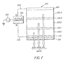
- FIG. 7 illustrates an example of a white light-emitting structure that can be used as an area lighting device or lamp 350.
- anode 210 is formed over transparent substrate 201.
- An alternating current source, 253, is connected to a DC / pulse converter 252 which provides current to the cathode 240 and anode 210 of the lamp via electrical conductors 260.
- organic EL unit 220.1 emits blue light
- organic EL unit 220.2 emits green light
- organic EL unit 220.3 emits red light.
- the intensity and exact hue of light emission from each organic EL unit is chosen so that they combine to yield white light, or nearly white light.
- Doped organic connectors 230.1 and 230.2 are as defined previously. There are many other combinations of organic EL units that can be used to yield light that appears white. For example, two-layer structures that emit blue and yellow light, or that emit red and cyan light, or that emit green and magenta light, can be used to generate white light. In all cases these units can be combined multiple times. For example, one can use several RGB stacks in a single device
- RGB filter is provided between the display and a viewer. This simplifies manufacturing because it is generally easier to apply a RGB filter after OLED device fabrication than to pattern RGB emitting pixels. While there are manufacturing advantages, this RGB filter method suffers greatly from lost efficiency since the filter wastes much of the generated light.
- a high efficiency RGB stack of this invention allows for the fabrication of a filtered RGB display that is not disadvantaged in terms of efficiency relative to a conventional patterned emissive RGB OLED of the prior art, and maintains the manufacturing advantage.
- FIGS 8 and 9 illustrate a non-limiting example of a matrix array of white light-emitting stacked OLED devices that can be used to fabricate a full-color matrix display.
- FIG. 8 is a cutaway schematic showing one example of electrical circuitry that can used to independently activate each stacked OLED device (that is, each pixel). This matrix array is commonly referred to as an active matrix array.
- the active matrix array is composed of X-direction signal lines X1, X2, X3, ..., Xn, Y-direction signal lines Y1, Y2, Y3,..., Ym, power supply (Vdd) lines Vdd1, Vdd2, Vdd3, ..., Vddn, thin-film transistors (TFTs) for switching TS11, TS21, TS31, ..., TS12, TS22, TS23, ..., TS31 , TS32, TS33, ..., TSnm, thin-film transistors (TFTs) for current control TC11, TC21, TC31, ..., TC12, TC22, TC23, TC31, TC32, TC33, ..., TCnm, stacked OLED devices EL11, EL21, EL31, ..., EL12, EL22, EL23, ..., EL31, EL32, EL33, ...,
- FIG. 9 is a cross-sectional schematic diagram illustrating three pixels of a full-color matrix display 600.
- Display 600 uses white light emission from an array of stacked organic electroluminescent devices (ELnm) and an array of color filters in registration with the devices. The color filters are situated between the devices and the viewer.
- transparent support 601 typically glass or quartz
- transparent organic insulator layers 602 and 603 Provided over transparent support 601 (typically glass or quartz), and the wiring, capacitors, and transistors necessary to drive the individual stacked OLED devices or pixels in the array.
- the electrical wiring, capacitors, and transistors in each pixel are designated by blocks ELEC11, ELEC12, and ELEC13, used to drive EL11, EL12, and EL13, respectively.
- organic insulator layer 602 Provided over organic insulator layer 602 is an array of optically transparent anode pads, 610, that are connected to ELEC11, ELEC12, and ELEC13 by conductive wiring 606, which may or may not be optically transparent.
- Organic insulator 603 is provided over organic insulator 602 and anode pads 610 and patterned to reveal the anode pads.
- white-light emitting organic layer 605 comprising a stack of two or more organic EL units and doped organic connectors as taught in this invention, necessary to yield white light emission. For example, a stack of red, green, and blue -emitting units, or a stack of blue and yellow-emitting units can all be effective.
- each organic EL unit can be deposited over the entire display device. This is followed by deposition of cathode 640, which is common to each stacked OLED device.
- cathode 640 which is common to each stacked OLED device.
- white light is emitted through the transparent anode 610, transparent organic insulator, 602, and through the transparent substrate 601.
- the emission area of each stacked OLED device (pixel) is defined by the contact area with the anode.
- red (651), green (652), and blue (653) filters that are positioned in registration with each pixel.
- Another application of this invention is in devices or displays that utilize blue emissive pixels and then use color conversion media filters to generate red and green light, thus making a full color display.
- blue-emitting OLEDs have historically been the least efficient and have had the worst lifetime.
- the efficiency and lifetime improvements of this invention (for example, a stack of blue-emitting organic EL units) can be used to great advantage in these devices.
- Full-color matrix display 660 has many of the same components as described previously for display 600, in FIG. 9, but utilizes an array of blue-emitting stacked organic electroluminescent devices and an array of color conversion filters in registration with the blue-emitting devices. The color conversion filters are situated between the devices and the viewer.
- blue light-emitting organic layer 665 includes a stack of two or more blue-emitting organic EL units.
- blue-to-red (661) and blue-to-green (662) color conversion filters that are positioned in registration with each pixel. These filters absorb blue light and fluoresce red or green. No filter is required in blue-emitting area 663, although it may include a transparent material or a blue trimming filter to adjust the hue. Thus, in FIG. 10, blue light generated by EL11 appears red, blue light generated by EL12 appears green, and blue light generated by EL13 appears blue. Materials and methods for depositing color conversion filter arrays on glass substrates are well-known in the art.
- Triplet emitter dopants such as Ir(ppy) 3 have been shown to have high efficiency when operated at low brightness. Unfortunately, when operated at higher brightness, the efficiency as well as the device life rapidly decreases.
- This invention (for example, a stack of organic EL units with triplet emitters) enables one to take full advantage of the high efficiency of triplet emitters by operating at low current density to achieve high brightness, without sacrificing stability.
- the organic EL units used in each stack can be selected to easily yield any color hue desired. The interactions between organic EL units are minimal in this regard.
- the present invention can be used in full-color matrix displays by making individual OLED stacks of all red, all green, and all blue organic EL units to serve as RGB pixels. That is, each organic EL unit in a stack is designed to emit essentially the same color.
- the greatly improved luminance efficiency can be used in many ways. For example, one can greatly increase the brightness of a full color display without sacrificing the stability of the device relative to a conventional OLED device.
- FIG. 11 A non-limiting example of this display configuration is shown in FIG. 11 and is driven by the same active matrix circuitry as described previously in FIG. 8.
- Full-color matrix display 680 has many of the same components as described previously for display 600, in FIG. 9. No filter array is required in matrix display 680.
- a matrix array of red (681), green (682), and blue (683) emitting organic layers are provided, each comprising a stack of two or more organic EL units of red, green, or blue, respectively. These organic layers are patterned over the device in registration with the anode pads. Thus, in FIG. 11, EL11 appears red, EL12 appears green, and EL13 appears blue.
- the stacked OLED device is typically provided over a supporting substrate where either the cathode or anode of the stacked OLED can be in contact with the substrate.
- the electrode in contact with the substrate is conveniently referred to as the bottom electrode.
- the bottom electrode is the anode, but this invention is not limited to that configuration.
- the substrate can either be light transmissive or opaque, depending on the intended direction of light emission. The light transmissive property is desirable for viewing the EL emission through the substrate. Transparent glass or plastic is commonly employed in such cases.
- the transmissive characteristic of the bottom support is immaterial, and therefore can be light transmissive, light absorbing or light reflective.
- Substrates for use in this case include, but are not limited to, glass, plastic, semiconductor materials, silicon, ceramics, and circuit board materials. Of course it is necessary to provide in these device configurations a light-transparent top electrode.
- anode When EL emission is viewed through anode 210, the anode should be transparent or substantially transparent to the emission of interest.
- Common transparent anode materials used in this invention are indium-tin oxide (ITO) and tin oxide, but other metal oxides can work including, but not limited to, aluminum- or indium-doped zinc oxide (IZO), magnesium-indium oxide, and nickel-tungsten oxide.
- ITO indium-tin oxide
- IZO aluminum- or indium-doped zinc oxide
- IZO aluminum- or indium-doped zinc oxide
- nickel-tungsten oxide nickel-tungsten oxide.
- metal nitrides such as gallium nitride
- metal selenides such as zinc selenide
- metal sulfides such as zinc sulfide
- the transmissive characteristics of anode are immaterial and any conductive material can be used, transparent, opaque or reflective.
- Example conductors for this application include, but are not limited to, gold, iridium, molybdenum, palladium, and platinum.
- Typical anode materials, transmissive or otherwise, have a work function of 4.1 eV or greater. Desired anode materials are commonly deposited by any suitable means such as evaporation, sputtering, chemical vapor deposition, or electrochemical means.
- Anodes can be patterned using well-known photolithographic processes.
- HIL Hole-Injecting Layer
- a hole-injecting layer 321 be provided between anode 210 and hole-transporting layer 323.
- the hole-injecting material can serve to improve the film formation property of subsequent organic layers and to facilitate injection of holes into the hole-transporting layer.
- Suitable materials for use in the hole-injecting layer include, but are not limited to, porphyrinic compounds as described in US-A-4,720,432, and plasma-deposited fluorocarbon polymers as described in US-A-6,208,075.
- Alternative hole-injecting materials reportedly useful in organic EL devices are described in EP 0 891 121 A1 and EP 1 029 909 A1.
- HTL Hole-Transporting Layer
- the hole-transporting layer 323 of the organic EL device contains at least one hole-transporting compound such as an aromatic tertiary amine, where the latter is understood to be a compound containing at least one trivalent nitrogen atom that is bonded only to carbon atoms, at least one of which is a member of an aromatic ring.
- the aromatic tertiary amine can be an arylamine, such as a monoarylamine, diarylamine, triarylamine, or a polymeric arylamine. Exemplary monomeric triarylamines are illustrated by Klupfel and others US-A-3,180,730.
- Other suitable triarylamines substituted with one or more vinyl radicals and/or comprising at least one active hydrogen containing group are disclosed by Brantley and others in US-A-3,567,450 and US-A-3,658,520.
- a more preferred class of aromatic tertiary amines are those which include at least two aromatic tertiary amine moieties as described in US-A-4,720,432 and US-A-5,061,569.
- Such compounds include those represented by structural formula (A). wherein Q 1 and Q 2 are independently selected aromatic tertiary amine moieties and G is a linking group such as an arylene, cycloalkylene, or alkylene group of a carbon to carbon bond.
- at least one of Q 1 or Q 2 contains a polycyclic fused ring structure, for example, a naphthalene.
- G is an aryl group, it is conveniently a phenylene, biphenylene, or naphthalene moiety.
- a useful class of triarylamines satisfying structural formula (A) and containing two triarylamine moieties is represented by structural formula (B): where
- tetraaryldiamines Another class of aromatic tertiary amines are the tetraaryldiamines. Desirable tetraaryldiamines include two diarylamino groups, such as indicated by formula (C), linked through an arylene group. Useful tetraaryldiamines include those represented by formula (D), wherein each Are may be an independently selected arylene group, such as a phenylene or anthracene moiety, n is an integer of from 1 to 4, and Ar, R 7 , R 8 , and R 9 are independently selected aryl groups. In a typical embodiment, at least one of Ar, R 7 , R 8 , and R 9 is a polycyclic fused ring structure, for example, a naphthalene
- the various alkyl, alkylene, aryl, and arylene moieties of the foregoing structural formulae (A), (B), (C), (D), can each in turn be substituted.
- Typical substituents include alkyl groups, alkenyl, alkoxy groups, aryl groups, aryloxy groups, and halogen such as fluoride, chloride, and bromide.
- the various alkyl and alkylene moieties typically contain from about 1 to 6 carbon atoms.
- the cycloalkyl moieties can contain from 3 to about 10 carbon atoms, but typically contain five, six, or seven ring carbon atoms ⁇ for example, cyclopentyl, cyclohexyl, and cycloheptyl ring structures.
- the aryl and arylene moieties are usually phenyl and phenylene moieties.
- the hole-transporting layer can be formed of a single or a mixture of aromatic tertiary amine compounds.
- a triarylamine such as a triarylamine satisfying the formula (B)
- a tetraaryldiamine such as indicated by formula (D).
- a triarylamine is employed in combination with a tetraaryldiamine, the latter is positioned as a layer interposed between the triarylamine and the electron injecting and transporting layer.
- useful aromatic tertiary amines are the following:
- Another class of useful hole-transporting materials includes polycyclic aromatic compounds as described in EP 1 009 041.
- polymeric hole-transporting materials can be used such as poly(N-vinylcarbazole) (PVK), polythiophenes, polypyrrole, polyaniline, and copolymers such as poly(3,4-ethylenedioxythiophene) / poly(4-styrenesulfonate) also called PEDOT/PSS.
- the light-emitting layer (LEL) 325 of the organic EL unit includes a luminescent or fluorescent material where electroluminescence is produced as a result of electron-hole pair recombination in this region.
- the light-emitting layer can be comprised of a single material, but more commonly consists of a host material doped with a guest compound or compounds where light emission comes primarily from the dopant and can be of any color.
- the host materials in the light-emitting layer can be an electron-transporting material, as defined below, a hole-transporting material, as defined above, or another material or combination of materials that support hole-electron recombination.
- the dopant is usually chosen from highly fluorescent dyes, but phosphorescent compounds, for example, transition metal complexes as described in WO 98/55561, WO 00/18851, WO 00/57676, and WO 00/70655 are also useful. Dopants are typically coated as 0.01 to 10 % by weight into the host material. Polymeric materials such as polyfluorenes and polyvinylarylenes (for example, poly(p-phenylenevinylene), PPV) can also be used as the host material. In this case, small molecule dopants can be molecularly dispersed into the polymeric host, or the dopant could be added by copolymerizing a minor constituent into the host polymer.
- Host and emitting molecules known to be of use include, but are not limited to, those disclosed in US-A-4,768,292; US-A-5,141,671; US-A-5,150,006; US-A-5,151,629; US-A-5,405,709; US-A-5,484,922; US-A-5,593,788; US-A-5,645,948; US-A-5,683,823; US-A-5,755,999; US-A-5,928,802; US-A-5,935,720; US-A-5,935,721; and US-A-6,020,078.
- Form E Metal complexes of 8-hydroxyquinoline and similar derivatives constitute one class of useful host compounds capable of supporting electroluminescence, and are particularly suitable for light emission of wavelengths longer than 500 nm, for example, green, yellow, orange, and red.
- the metal can be monovalent, divalent, trivalent, or tetravalent metal.
- the metal can, for example, be an alkali metal, such as lithium, sodium, or potassium; an alkaline earth metal, such as magnesium or calcium; an earth metal, such aluminum or gallium, or a transition metal such as zinc or zirconium.
- alkali metal such as lithium, sodium, or potassium
- alkaline earth metal such as magnesium or calcium
- earth metal such aluminum or gallium, or a transition metal such as zinc or zirconium.
- any monovalent, divalent, trivalent, or tetravalent metal known to be a useful chelating metal can be employed.
- Z completes a heterocyclic nucleus containing at least two fused aromatic rings, at least one of which is an azole or azine ring. Additional rings, including both aliphatic and aromatic rings, can be fused with the two required rings, if required. To avoid adding molecular bulk without improving on function the number of ring atoms is usually maintained at 18 or less.
- Illustrative of useful chelated oxinoid compounds are the following:
- Formula F Derivatives of 9,10-di-(2-naphthyl)anthracene (Formula F) constitute one class of useful hosts capable of supporting electroluminescence, and are particularly suitable for light emission of wavelengths longer than 400 nm, for example, blue, green, yellow, orange or red.
- R 1 , R 2 , R 3 , R 4 , R 5 , and R 6 represent one or more substituents on each ring where each substituent may be individually selected from the following groups:
- Illustrative examples include 9,10-di-(2-naphthyl)anthracene and 2- t -butyl-9,10-di-(2-naphthyl)anthracene.
- Other anthracene derivatives can be useful as a host in the LEL, including derivatives of 9,10-bis[4-(2,2-diphenylethenyl)phenyl]anthracene.
- Benzazole derivatives constitute another class of useful hosts capable of supporting electroluminescence, and are particularly suitable for light emission of wavelengths longer than 400 nm, for example, blue, green, yellow, orange or red.
- An example of a useful benzazole is 2, 2', 2"-(1,3,5-phenylene)tris[1-phenyl-1H-benzimidazole].
- Distyrylarylene derivatives as described in US-A-5,121,029 are also useful host material for the LEL.
- Desirable fluorescent dopants include derivatives of anthracene, tetracene, xanthene, perylene, rubrene, coumarin, rhodamine, quinacridone, dicyanomethylenepyran compounds, thiopyran compounds, polymethine compounds, pyrilium and thiapyrilium compounds, fluorene derivatives, periflanthene derivatives, and carbostyryl compounds.
- Illustrative examples of useful dopants include, but are not limited to, the following:
- ETL Electron-Transporting Layer
- Preferred thin film-forming materials for use in forming the electron-transporting layer 327 of the organic EL devices of this invention are metal chelated oxinoid compounds, including chelates of oxine itself (also commonly referred to as 8-quinolinol or 8-hydroxyquinoline). Such compounds help to inject and transport electrons and exhibit both high levels of performance and are readily fabricated in the form of thin films.
- exemplary of contemplated oxinoid compounds are those satisfying structural formula (E), previously described.
- electron-transporting materials include various butadiene derivatives as disclosed in US-A-4,356,429 and various heterocyclic optical brighteners as described in US-A-4,539,507.
- Benzazoles satisfying structural formula (G) are also useful electron-transporting materials.
- layers 327 and 325 can optionally be collapsed into a single layer that serves the function of supporting both light emission and electron transport. These layers can be collapsed in both small molecule OLED systems and in polymeric OLED systems.
- a hole-transporting layer such as PEDOT-PSS with a polymeric light-emitting layer such as PPV.
- PPV serves the function of supporting both light emission and electron transport.
- the cathode 240 used in this invention can be comprised of nearly any conductive material. Desirable materials have good film-forming properties to ensure good contact with the underlying organic layer, promote electron injection at low voltage, and have good stability. Useful cathode materials often contain a low work function metal ( ⁇ 4.0 eV) or metal alloy.
- One preferred cathode material is comprised of a Mg:Ag alloy wherein the percentage of silver is in the range of 1 to 20 %, as described in US-A-4,885,221.
- cathode materials includes bilayers comprising a thin electron-injection layer (EIL) 329 in contact with the organic layer (for example, ETL) which is capped with a thicker layer of a conductive metal.
- EIL electron-injection layer
- the EIL preferably includes a low work function metal or metal salt, and if so, the thicker capping layer does not need to have a low work function.
- One such cathode is comprised of a thin layer of LiF followed by a thicker layer of Al as described in US-A-5,677,572.
- Other useful cathode material sets include, but are not limited to, those disclosed in US-A-5,059,861; US-A-5,059,862, and US-A-6,140,763.
- cathode When light emission is viewed through the cathode, the cathode must be transparent or nearly transparent. For such applications, metals must be thin or one must use transparent conductive oxides, or a combination of these materials.
- Optically transparent cathodes have been described in more detail in US-A-5,776,623. Cathode materials can be deposited by evaporation, sputtering, or chemical vapor deposition. When needed, patterning can be achieved through many well known methods including, but not limited to, through-mask deposition, integral shadow masking as described in US-A-5,276,380 and EP 0 732 868, laser ablation, and selective chemical vapor deposition.
- the organic materials mentioned above are suitably deposited through a vapor-phase method such as sublimation, but can be deposited from a fluid, for example, from a solvent with an optional binder to improve film formation. If the material is a polymer, solvent deposition is useful but other methods can be used, such as sputtering or thermal transfer from a donor sheet.
- the material to be deposited by sublimation can be vaporized from a sublimator "boat" often comprised of a tantalum material, for example, as described in US-A-6,237,529, or can be first coated onto a donor sheet and then sublimed in closer proximity to the substrate.
- Layers with a mixture of materials can utilize separate sublimator boats or the materials can be pre-mixed and coated from a single boat or donor sheet. Patterned deposition can be achieved using shadow masks, integral shadow masks (US-A-5,294,870), spatially-defined thermal dye transfer from a donor sheet (US-A-5,851,709 and US-A-6,066,357) and inkjet method (US-A-6,066,357).
- OLED devices are sensitive to moisture or oxygen, or both, so they are commonly sealed in an inert atmosphere such as nitrogen or argon, along with a desiccant such as alumina, bauxite, calcium sulfate, clays, silica gel, zeolites, alkaline metal oxides, alkaline earth metal oxides, sulfates, or metal halides and perchlorates.
- a desiccant such as alumina, bauxite, calcium sulfate, clays, silica gel, zeolites, alkaline metal oxides, alkaline earth metal oxides, sulfates, or metal halides and perchlorates.
- Methods for encapsulation and desiccation include, but are not limited to, those described in US-A-6,226,890.
- barrier layers such as SiOx, Teflon, and alternating inorganic/polymeric layers are known in the art for encapsulation.
- Stacked OLED devices of this invention can employ various well-known optical effects in order to enhance its properties if desired. This includes optimizing layer thicknesses to yield maximum light transmission, providing dielectric mirror structures, replacing reflective electrodes with light-absorbing electrodes, providing anti glare or anti-reflection coatings over the display, providing a polarizing medium over the display, or providing colored or neutral density filters over the display.
- the electroluminescence characteristics of all the fabricated devices were evaluated using a constant current source and a photometer at room temperature.
- Example 1 (Conventional OLED - comparative):
- the preparation of a conventional non-stacked OLED is as follows: A 1mm thick glass substrate coated with a transparent ITO conductive layer was cleaned and dried using a commercial glass scrubber tool. The thickness of ITO is about 42 nm and the sheet resistance of the ITO is about 68 ⁇ /square. The ITO surface was subsequently treated with oxidative plasma to condition the surface as an anode. A layer of CFx, 1 nm thick, was deposited on the clean ITO surface as the HIL by decomposing CHF 3 gas in RF plasma treatment chamber. The substrate was then transferred into a vacuum deposition chamber for deposition of all other layers on top of the substrate. The following layers were deposited in the following sequence by sublimation from a heated boat under a vacuum of approximately 10 -6 Torr:
- the device was transferred from the deposition chamber into a dry box for encapsulation.
- the completed device structure is denoted as ITO/CFx/NPB(75)/Alq(60)/Mg:Ag.
- This device requires a driving voltage of 6.2 V to pass 20 mA/cm 2 . Its luminance efficiency is 2.4 cd/A.
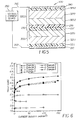
- the luminance efficiency-current characteristic, indicated as Example 1, is shown in FIG. 6.
- a stacked OLED was fabricated with the following sequential layers:
- the processing steps other than the aforementioned layer deposition were the same as Example 1.
- the stacked device structure is denoted as ITO/CFx/NPB(50)/Alq(50)/ Mg:Ag / Ag /NPB(50)/Alq(50)/Mg:Ag.
- This stacked OLED requires a driving voltage of 21.2 V to pass 20 mA/cm 2 . Its EL efficiency is 0.1 cd/A. Its luminance efficiency-current characteristic, indicated as Example 2, is shown in FIG. 6
- a stacked OLED was fabricated with the following sequential layers:
- Example 1 The processing steps other than the aforementioned layer deposition were the same as Example 1.
- the stacked device structure is denoted as ITO/CFx/NPB(75)/Alq(60)/ Mg /NPB(75)/Alq(60)/Mg:Ag
- the stacked OLED has a driving voltage of 11.2 V, a current density of 20 mA/cm 2 , and an EL efficiency of 1.3 cd/A. Its luminance efficiency-current characteristic, indicated as Example 3, is shown in FIG. 6.
- a stacked OLED was fabricated, which was similar to Example 3 except there was no metal electrode in between the two EL units.
- the stacked device structure is denoted as ITO/CFx/NPB(75)/Alq(60)/NPB(75)/Alq(60)/Mg:Ag.
- the stacked OLED requires a very high driving voltage (29 V) in order to pass a current density of 20 mA/cm 2 .
- the corresponding EL efficiency is 3.1 cd/A. Its luminance efficiency-current characteristic, indicated as Example 4, is shown in FIG. 6.
- Comparative Examples 2, 3, and 4 clearly show that the connection between adjacent organic EL units is very critical in making stacked OLED that is more efficient than the non-stacked OLED.
- a thin metal intra-electrode layer as described in the prior art apparently can cause transmission loss due to optical absorption and reflection, as well as carrier injection difficulty when placed in between the organic EL units. Optical absorption could be reduced without any electrode in between the EL units but carrier injection barrier between each organic EL unit would still be very high, as evidenced by the very high driving voltage.
- a stacked OLED was fabricated with the following sequential layers:
- Example 1 The processing steps other than the aforementioned layer deposition were the same as Example 1.
- the stacked device structure is denoted as ITO/CFx/ NPB(75)/Alq(55)/ Alq:n-dopant(5) / NPB:p-dopant(5) /NPB(70)/Alq(60)/Mg:Ag.
- the stacked OLED has a driving voltage of 18.5 V, a current density of 20 mA/cm 2 , and an EL efficiency of 3.9 cd/A. Its luminance efficiency-current characteristic, indicated as Example 5, is shown in FIG. 6.
- a stacked OLED was fabricated with the following sequential layers:
- Example 1 The processing steps other than the aforementioned layer deposition were the same as Example 1.
- the stacked device structure is denoted as ITO/CFx/NPB(75)/Alq(60)/ NPB:p-dopant(5) /NPB(70)/Alq(60)/Mg:Ag.
- the stacked OLED has a driving voltage of 17.7 V, a current density of 20 mA/cm 2 , and an EL efficiency of 4.0 cd/A.
- the luminance efficiency-current characteristic, indicated as Example 6, is shown in FIG. 6.
- the processing steps other than the aforementioned layer deposition were the same as Example 1.
- the stacked device structure is also denoted as ITO/CFx/NPB(75)/Alq(30)/ NPB:p-dopant(5) /NPB(25)/Alq(60)/Mg:Ag.
- the luminance efficiency-current characteristic of the stacked OLED is shown in FIG. 6, indicated as Example 7.
- This optimized device has a driving voltage of 12V, current density of 20 mA/cm 2 , and an EL efficiency of 4.9 cd/A. It shows that, by stacking two organic EL units in one OLED serially, double luminance efficiency could be obtained (with doubled driving voltage). Since the luminance is proportional to the current density, this stacked OLED device could be operated to produce twice the luminance output of the reference OLED (Example 1) for the same current density. Therefore, the lifetime of the stacked OLED could be increased by a factor of 2 with no sacrifice in luminance.
- This example demonstrates that by stacking multiple organic EL units together with the doped organic connectors as described in this invention, further improvements in luminance efficiency can be achieved.
- the stacked organic electroluminescent device wherein all of the organic electroluminescent units are the same.
- the stacked organic electroluminescent device wherein at least one of the organic electroluminescent units is different from at least one other.
- the stacked organic electroluminescent device wherein at least one of the doped organic connectors is different from at least one other doped organic connector.
- the stacked organic electroluminescent device wherein at least one of the organic electroluminescent units comprises a triplet emitter.
- each organic electroluminescent unit is from 2 to 200 nm.
- a full-color matrix display that is observable by a viewer comprising:
- a full-color matrix display that is observable by a viewer comprising:
- a stacked organic electroluminescent device comprising:
- the stacked organic electroluminescent device wherein the n-type doped organic layer comprises at least one host organic material and at least one n-type dopant, wherein the host organic material is capable of supporting electron transport.
- the stacked organic electroluminescent device wherein the host organic material of the n-type doped organic layer includes metal chelated oxinoid compounds, 8-hydroxyquinoline derivatives, butadiene derivatives, heterocyclic optical brighteners, triazines, benzazoles, or silole derivatives, or combinations thereof.
- the stacked organic electroluminescent device wherein the n-type dopant in the n-type doped organic layer has a work function less than 4.0 eV.
- the stacked organic electroluminescent device wherein the n-type dopant in the n-type doped organic layer comprises alkali metals, alkali metal compounds, alkaline earth metals, or alkaline metal compounds, or combinations thereof.
- the stacked organic electroluminescent device wherein the n-type dopant in the n-type doped organic layer includes organic reducing agents with strong electron-donating properties such that they are capable of forming charge-transfer complexes with the organic host material.
- the stacked organic electroluminescent device wherein the n-type dopant in the n-type doped organic layer includes bis(ethylenedithio)-tetrathiafulvalene (BEDT-TTF), tetrathiafulvalene (TTF), or their derivatives, or combinations thereof.
- BEDT-TTF bis(ethylenedithio)-tetrathiafulvalene
- TTF tetrathiafulvalene
- the stacked organic electroluminescent device wherein the n-type doped concentration is in the range of 0.01 ⁇ 10 vol. %.
- each organic electroluminescent unit is from 2 to 200 nm.
- each doped organic connector is from 1 to 100 nm.
- the stacked organic electroluminescent device wherein the organic electroluminescent units comprise small molecule materials.
- the stacked organic electroluminescent device wherein the organic electroluminescent units comprise a hole-transporting layer and an electron-transporting layer.
- the stacked organic electroluminescent device wherein the organic electroluminescent units comprise polymeric materials.
- the stacked organic electroluminescent device wherein the organic electroluminescent units comprise a hole-transporting layer and a light-emitting layer.
- the stacked organic electroluminescent device comprising at least three organic electroluminescent units such that red, green, and blue-emitting units are combined to yield white light.
- the stacked organic electroluminescent device wherein the organic electroluminescent units emit essentially the same color.
- a stacked organic electroluminescent device comprising:
- the stacked organic electroluminescent device wherein the p-type doped organic layer comprises at least one host organic material and at least one p-type dopant, wherein the host organic material is capable of supporting hole transport.
- the stacked organic electroluminescent device wherein the host organic material of the p-type doped organic layer includes aromatic tertiary amines having at least one trivalent nitrogen atom that is bonded only to carbon atoms, at least one of which is a member of an aromatic ring.
- the stacked organic electroluminescent device wherein the p-type dopant in the p-type doped organic layer includes inorganic oxidizing agents capable of forming a charge transfer complex with the host material.
- the stacked organic electroluminescent device where the p-type dopant in the p-type doped organic layer includes iodine, FeCl 3 , or SbCl 5 , or combinations thereof.
- the stacked organic electroluminescent device wherein the p-type dopant in the p-type doped organic layer includes organic oxidizing agents with strong electron-withdrawing properties such as are capable of forming a charge transfer complex with the host material.
- the stacked organic electroluminescent device wherein the p-type dopant in the p-type doped organic layer includes 2,3,5,6-tetrafluoro-7,7,8,8-tetracyanoquinodimethane (F 4 -TCNQ) or other derivatives of TCNQ, or combinations thereof.
- the stacked organic electroluminescent device wherein the p-type doped concentration is in the range of 0.01 ⁇ 10 vol. %.
- each organic electroluminescent unit is from 2 to 200 nm.
- each doped organic connector is from 1 to 100 nm.
- the stacked organic electroluminescent device wherein the organic electroluminescent units comprise small molecule materials.
- the stacked organic electroluminescent device wherein the organic electroluminescent units comprise a hole-transporting layer and an electron-transporting layer.
- the stacked organic electroluminescent device wherein the organic electroluminescent units comprise polymeric materials.
- the stacked organic electroluminescent device wherein the organic electroluminescent units comprise a hole-transporting layer and a light-emitting layer.
- the stacked organic electroluminescent device comprising at least three organic electroluminescent units such that red, green, and blue-emitting units are combined to yield white light.
- the stacked organic electroluminescent device wherein the organic electroluminescent units emit essentially the same color.
- a stacked organic electroluminescent device comprising:
- the stacked organic electroluminescent device wherein the doped organic connector comprises an n-type doped organic layer and a p-type doped organic layer disposed adjacent to one another, wherein the n-type doped organic layer is disposed towards the anode side, and the p-type doped organic layer is disposed towards the cathode side.
- the stacked organic electroluminescent device wherein the n-type doped organic layer comprises at least one host organic material and at least one n-type dopant, wherein the host organic material for the n-type doped organic layer is capable of supporting electron transport, and wherein the p-type doped organic layer comprises at least one host organic material and at least one p-type dopant, wherein the host organic material for the p-type doped organic layer is capable of supporting hole transport.
- the stacked organic electroluminescent device wherein the host organic material of the n-type doped organic layer includes metal chelated oxinoid compounds, 8-hydroxyquinoline derivatives, butadiene derivatives, heterocyclic optical brighteners, triazines, benzazoles, or silole derivatives, or combinations thereof.
- the stacked organic electroluminescent device wherein the n-type dopant in the n-type doped organic layer has a work function less than 4.0 eV.
- the stacked organic electroluminescent device wherein the n-type dopant in the n-type doped organic layer comprises alkali metals, alkali metal compounds, alkaline earth metals, or alkaline metal compounds, or combinations thereof.
- the stacked organic electroluminescent device wherein the n-type dopant in the n-type doped organic layer includes organic reducing agents with strong electron-donating properties, capable of forming charge-transfer complexes with the organic host material.
- the stacked organic electroluminescent device wherein the n-type dopant in the n-type doped organic layer includes bis(ethylenedithio)-tetrathiafulvalene (BEDT-TTF), tetrathiafulvalene (TTF), or their derivatives, or combinations thereof.
- BEDT-TTF bis(ethylenedithio)-tetrathiafulvalene
- TTF tetrathiafulvalene
- the stacked organic electroluminescent device wherein the host organic material of the p-type doped organic layer includes aromatic tertiary amines having at least one trivalent nitrogen atom that is bonded only to carbon atoms, at least one of which is a member of an aromatic ring.
- the stacked organic electroluminescent device wherein the p-type dopant in the p-type doped organic layer includes inorganic oxidizing agents capable of forming a charge transfer complex with the host material.
- the stacked organic electroluminescent device where the p-type dopant in the p-type doped organic layer includes iodine, FeCl 3 , or SbCl 5 , or combinations thereof.
- the stacked organic electroluminescent device wherein the p-type dopant in the p-type doped organic layer includes organic oxidizing agents with strong electron-withdrawing properties, capable of forming a charge transfer complex with the host material.
- the stacked organic electroluminescent device wherein the p-type dopant in the p-type doped organic layer includes 2,3,5,6-tetrafluoro-7,7,8,8-tetracyanoquinodimethane (F 4 -TCNQ) or other derivatives of TCNQ, or combinations thereof.
- the stacked organic electroluminescent device wherein both the n-type and p-type doped concentration is in the range of 0.01 ⁇ 10 vol. %.
- each organic electroluminescent unit is from 2 to 200 nm.
- each doped organic connector is from 1 to 100 nm.
- the stacked organic electroluminescent device wherein the organic electroluminescent units comprise small molecule materials.
- the stacked organic electroluminescent device wherein the organic electroluminescent units comprise a hole-transporting layer and an electron-transporting layer.
- the stacked organic electroluminescent device wherein the organic electroluminescent units comprise polymeric materials.
- the stacked organic electroluminescent device wherein the organic electroluminescent units comprise a hole-transporting layer and an electron-transporting layer.
- the stacked organic electroluminescent device comprising at least three organic electroluminescent units such that red, green, and blue-emitting units are combined to yield white light.
- the stacked organic electroluminescent device wherein the organic electroluminescent units emit essentially the same color.
- a method of making a stacked organic electroluminescent device having at least two organic electroluminescent units comprising the steps of:
- the method further including one or more intermediate organic electroluminescent unit(s) disposed between the first and second organic electroluminescent units, with each such intermediate organic electroluminescent unit being formed without an anode or a cathode and using a doped organic connector to secure such intermediate organic electroluminescent unit(s) within the stacked organic electroluminescent device.
- the method further including the step of selecting the organic electroluminescent units to provide improved luminance efficiency.
Landscapes
- Physics & Mathematics (AREA)
- Optics & Photonics (AREA)
- Electroluminescent Light Sources (AREA)
- Control Of Indicators Other Than Cathode Ray Tubes (AREA)
Applications Claiming Priority (2)
| Application Number | Priority Date | Filing Date | Title |
|---|---|---|---|
| US77270 | 1993-06-17 | ||
| US10/077,270 US6872472B2 (en) | 2002-02-15 | 2002-02-15 | Providing an organic electroluminescent device having stacked electroluminescent units |
Publications (3)
| Publication Number | Publication Date |
|---|---|
| EP1339112A2 true EP1339112A2 (de) | 2003-08-27 |
| EP1339112A3 EP1339112A3 (de) | 2006-09-13 |
| EP1339112B1 EP1339112B1 (de) | 2011-09-28 |
Family
ID=27660276
Family Applications (1)
| Application Number | Title | Priority Date | Filing Date |
|---|---|---|---|
| EP03075309A Expired - Lifetime EP1339112B1 (de) | 2002-02-15 | 2003-02-03 | Organische elektrolumineszente Anordnung mit gestapelten elektrolumineszenten Elementen |
Country Status (6)
| Country | Link |
|---|---|
| US (2) | US6872472B2 (de) |
| EP (1) | EP1339112B1 (de) |
| JP (1) | JP4570014B2 (de) |
| KR (1) | KR100911555B1 (de) |
| CN (1) | CN100483728C (de) |
| TW (1) | TWI264240B (de) |
Cited By (49)
| Publication number | Priority date | Publication date | Assignee | Title |
|---|---|---|---|---|
| WO2005069398A3 (en) * | 2004-01-05 | 2005-12-29 | Eastman Kodak Co | Method of making an oled device |
| EP1555701A3 (de) * | 2004-01-16 | 2006-01-18 | Novaled GmbH | Bildelement für eine Aktiv-Matrix-Anzeige |
| WO2006023322A1 (en) * | 2004-08-20 | 2006-03-02 | Eastman Kodak Company | White oled having multiple white electroluminescent units |
| WO2006033285A1 (en) | 2004-09-24 | 2006-03-30 | Semiconductor Energy Laboratory Co., Ltd. | Light emitting device |
| GB2426856A (en) * | 2005-05-20 | 2006-12-06 | Lg Philips Lcd Co Ltd | Stacked OLED structure having mixed region |
| WO2007005325A1 (en) * | 2005-06-29 | 2007-01-11 | Eastman Kodak Company | Broadband light tandem oled display |
| WO2007005200A1 (en) | 2005-06-29 | 2007-01-11 | Eastman Kodak Company | White light tandem oled display with filters |
| EP1753269A1 (de) * | 2005-08-12 | 2007-02-14 | Samsung SDI Co., Ltd. | Weiss-elektrolumineszierende Vorrichtung und derren Herstellungsverfahren |
| EP1376714A3 (de) * | 2002-06-28 | 2007-02-14 | Semiconductor Energy Laboratory Co., Ltd. | Lichtemittierende Vorrichtung und Herstellungsverfahren |
| WO2007071451A1 (en) * | 2005-12-23 | 2007-06-28 | Novaled Ag | An organic light emitting device with a plurality of organic electroluminescent units stacked upon each other |
| WO2007071450A1 (en) * | 2005-12-23 | 2007-06-28 | Novaled Ag | Electronic device with a layer structure of organic layers |
| EP1804308A1 (de) * | 2005-12-23 | 2007-07-04 | Novaled AG | Organische lichtemittierende Vorrichtung mit mehreren aufeinander gestapelten organischen elektrolumineszenten Einheiten |
| EP1804309A1 (de) * | 2005-12-23 | 2007-07-04 | Novaled AG | Elektronische Vorrichtung mit einer Schichtenstruktur von organischen Schichten |
| US7291969B2 (en) | 2002-08-09 | 2007-11-06 | Semiconductor Energy Laboratory Co., Ltd. | Organic electroluminescent device |
| US7420203B2 (en) | 2001-12-05 | 2008-09-02 | Semiconductor Energy Laboratory Co., Ltd. | Organic semiconductor element |
| US7449830B2 (en) | 2004-08-02 | 2008-11-11 | Lg Display Co., Ltd. | OLEDs having improved luminance stability |
| US7449831B2 (en) | 2004-08-02 | 2008-11-11 | Lg Display Co., Ltd. | OLEDs having inorganic material containing anode capping layer |
| WO2009005597A1 (en) * | 2007-06-27 | 2009-01-08 | Eastman Kodak Company | Improved tandem oled device |
| WO2009053088A1 (de) * | 2007-10-24 | 2009-04-30 | Merck Patent Gmbh | Optoelektronische vorrichtung |
| EP1784055A3 (de) * | 2005-10-17 | 2009-08-05 | Semiconductor Energy Laboratory Co., Ltd. | Beleuchtungssystem |
| US7598670B2 (en) | 2004-05-21 | 2009-10-06 | Semiconductor Energy Laboratory Co., Ltd. | Light emitting element and light emitting device |
| EP1705729A3 (de) * | 2005-03-02 | 2009-12-09 | OSRAM Opto Semiconductors GmbH | Hybride Lichtquelle auf Basis von Polymeren und kleinen Molekülen |
| US7663140B2 (en) | 2004-05-21 | 2010-02-16 | Semiconductor Energy Laboratory Co., Ltd. | Light emitting element and light emitting device using the element |
| US7692380B2 (en) | 2002-04-05 | 2010-04-06 | Semiconductor Energy Laboratory Co., Ltd. | Light emitting device including plural barriers |
| WO2010062643A1 (en) * | 2008-10-28 | 2010-06-03 | The Regents Of The University Of Michigan | Stacked white oled having separate red, green and blue sub-elements |
| US7811679B2 (en) | 2005-05-20 | 2010-10-12 | Lg Display Co., Ltd. | Display devices with light absorbing metal nanoparticle layers |
| EP1866984A4 (de) * | 2005-03-23 | 2010-11-24 | Semiconductor Energy Lab | Zusammengesetztes material, lichtemittierendes element und lichtemittierende einrichtung |
| EP1743508A4 (de) * | 2004-04-09 | 2011-04-27 | Lg Chemical Ltd | Geschichtete organische lichtemittierende vorrichtung mit hoher leistung und hoher leuchtkraft |
| US7943244B2 (en) | 2005-05-20 | 2011-05-17 | Lg Display Co., Ltd. | Display device with metal-organic mixed layer anodes |
| EP1983805A4 (de) * | 2006-02-07 | 2011-05-18 | Sumitomo Chemical Co | Organisches elektrolumineszenzelement |
| US7964891B2 (en) | 2004-08-04 | 2011-06-21 | Semiconductor Energy Laboratory Co., Ltd. | Light-emitting element, display device, and electronic appliance |
| US8018152B2 (en) | 2004-05-20 | 2011-09-13 | Semiconductor Energy Laboratory Co., Ltd. | Light-emitting element including intermediate conductive layer having a hole-injection layer with an island-like structure |
| US8040044B2 (en) | 2005-07-15 | 2011-10-18 | Lg Chem, Ltd. | Organic light emitting device and method for manufacturing the same |
| EP2330651A3 (de) * | 2009-12-04 | 2011-10-26 | Samsung Mobile Display Co., Ltd. | Organische lichtemittierende Diodenvorrichtung |
| EP1845568A3 (de) * | 2006-04-13 | 2012-03-21 | LG Display Co., Ltd. | Organische elektrolumineszente Vorrichtung und Herstellungsverfahren dafür |
| US8487527B2 (en) | 2005-05-04 | 2013-07-16 | Lg Display Co., Ltd. | Organic light emitting devices |
| EP1930969A3 (de) * | 2006-12-04 | 2013-11-20 | Semiconductor Energy Laboratory Co., Ltd. | Lichtemittierendes Element, lichtemittierende Vorrichtung und elektronische Vorrichtung |
| WO2014020817A1 (en) * | 2012-07-31 | 2014-02-06 | Sony Corporation | Display apparatus, method of manufacturing a display apparatus, electronic appliance, and method of driving a display apparatus |
| US8912718B2 (en) | 2004-09-13 | 2014-12-16 | Semiconductor Energy Laboratory Co., Ltd. | Light emitting device with a plurality of circuits connected in parallel |
| CN104319355A (zh) * | 2014-11-20 | 2015-01-28 | 京东方科技集团股份有限公司 | 一种发光器件及其驱动控制方法、灯具 |
| EP2437100A4 (de) * | 2009-05-29 | 2015-05-20 | Neoviewkolon Co Ltd | Anzeigevorrichtung |
| WO2016030331A1 (de) * | 2014-08-25 | 2016-03-03 | Osram Oled Gmbh | Organisches licht emittierendes bauelement und verfahren zur herstellung eines organischen licht emittierenden bauelements |
| US9478593B2 (en) | 2011-11-04 | 2016-10-25 | Semiconductor Energy Laboratory Co., Ltd. | Light-emitting module and light-emitting device |
| DE102006023512B4 (de) * | 2005-05-20 | 2017-03-09 | Lg Display Co., Ltd. | Zwischenelektroden für gestapelte OLEDs |
| US9802710B2 (en) | 2013-05-06 | 2017-10-31 | Airbus Operations Gmbh | Passenger supply system for installation in a passenger supply channel |
| EP3249695A1 (de) * | 2016-05-25 | 2017-11-29 | Samsung Display Co., Ltd. | Organische lichtemittierende anzeige |
| US10505120B2 (en) | 2011-02-28 | 2019-12-10 | Semiconductor Energy Laboratory Co., Ltd. | Light-emitting device |
| WO2021154690A1 (en) * | 2020-01-28 | 2021-08-05 | OLEDWorks LLC | Stacked oled microdisplay with low-voltage silicon backplane |
| DE102011116661B4 (de) | 2010-10-22 | 2021-08-12 | Lg Display Co., Ltd. | Organische leuchtdiodenvorrichtung |
Families Citing this family (320)
| Publication number | Priority date | Publication date | Assignee | Title |
|---|---|---|---|---|
| JP3875401B2 (ja) * | 1998-05-12 | 2007-01-31 | Tdk株式会社 | 有機el表示装置及び有機el素子 |
| JP3884564B2 (ja) * | 1998-05-20 | 2007-02-21 | 出光興産株式会社 | 有機el発光素子およびそれを用いた発光装置 |
| KR100888424B1 (ko) * | 2001-05-16 | 2009-03-11 | 더 트러스티즈 오브 프린스턴 유니버시티 | 고효율 다칼라 전기 유기 발광 장치 |
| GB0118791D0 (en) * | 2001-08-01 | 2001-09-26 | Cambridge Display Tech Ltd | Multi-step organic light-emissive devices |
| US8153184B2 (en) * | 2001-11-26 | 2012-04-10 | Samsung Mobile Display Co., Ltd. | Organic EL display device and method of manufacturing the same |
| KR100656490B1 (ko) * | 2001-11-26 | 2006-12-12 | 삼성에스디아이 주식회사 | 풀칼라 유기전계 발광표시소자 및 그의 제조방법 |
| JP2007027141A (ja) * | 2001-12-05 | 2007-02-01 | Semiconductor Energy Lab Co Ltd | 有機半導体素子の作製方法 |
| JP2005123208A (ja) * | 2001-12-05 | 2005-05-12 | Semiconductor Energy Lab Co Ltd | 有機太陽電池 |
| US6872472B2 (en) * | 2002-02-15 | 2005-03-29 | Eastman Kodak Company | Providing an organic electroluminescent device having stacked electroluminescent units |
| US7358658B2 (en) * | 2002-03-08 | 2008-04-15 | Chien-Min Sung | Amorphous diamond materials and associated methods for the use and manufacture thereof |
| JP3933591B2 (ja) | 2002-03-26 | 2007-06-20 | 淳二 城戸 | 有機エレクトロルミネッセント素子 |
| US8932730B2 (en) * | 2002-04-08 | 2015-01-13 | The University of Northern California | Doped organic carrier transport materials |
| EP1367659B1 (de) * | 2002-05-21 | 2012-09-05 | Semiconductor Energy Laboratory Co., Ltd. | Organischer Feldeffekt-Transistor |
| EP1418634A1 (de) * | 2002-11-06 | 2004-05-12 | Samsung SDI Co. Ltd. | Display auf Basis organischer, lichtemittierender Bauelemente (OLED) mit niederohmigem Kathodenkontakt |
| WO2004060026A1 (ja) | 2002-12-26 | 2004-07-15 | Semiconductor Energy Laboratory Co., Ltd. | 有機発光素子 |
| CN1742518B (zh) * | 2003-01-29 | 2010-09-29 | 株式会社半导体能源研究所 | 发光装置 |
| JP2004288624A (ja) * | 2003-03-03 | 2004-10-14 | Sanyo Electric Co Ltd | エレクトロルミネッセンス表示装置 |
| JP4531342B2 (ja) * | 2003-03-17 | 2010-08-25 | 株式会社半導体エネルギー研究所 | 白色有機発光素子および発光装置 |
| US7333072B2 (en) * | 2003-03-24 | 2008-02-19 | Semiconductor Energy Laboratory Co., Ltd. | Thin film integrated circuit device |
| TWI363573B (en) * | 2003-04-07 | 2012-05-01 | Semiconductor Energy Lab | Electronic apparatus |
| US7862906B2 (en) * | 2003-04-09 | 2011-01-04 | Semiconductor Energy Laboratory Co., Ltd. | Electroluminescent element and light-emitting device |
| WO2004095892A1 (ja) * | 2003-04-24 | 2004-11-04 | Idemitsu Kosan Co., Ltd. | 有機エレクトロルミネッセンス素子及び表示装置 |
| US6903378B2 (en) * | 2003-06-26 | 2005-06-07 | Eastman Kodak Company | Stacked OLED display having improved efficiency |
| US7622863B2 (en) * | 2003-06-30 | 2009-11-24 | Semiconductor Energy Laboratory Co., Ltd. | Light-emitting device and electronic device including first and second light emitting elements |
| ATE532386T1 (de) * | 2003-07-02 | 2011-11-15 | Idemitsu Kosan Co | Organisches elektrolumineszenz-bauelement und display damit |
| US7675230B2 (en) * | 2003-07-10 | 2010-03-09 | Ideal Star Inc. | Light-emitting element and device |
| US7504049B2 (en) * | 2003-08-25 | 2009-03-17 | Semiconductor Energy Laboratory Co., Ltd. | Electrode device for organic device, electronic device having electrode device for organic device, and method of forming electrode device for organic device |
| US7511421B2 (en) * | 2003-08-25 | 2009-03-31 | Semiconductor Energy Laboratory Co., Ltd. | Mixed metal and organic electrode for organic device |
| DE10353036B4 (de) | 2003-11-13 | 2021-11-25 | Pictiva Displays International Limited | Vollfarbige organische Anzeige mit Farbfiltertechnologie und angepasstem weißen Emittermaterial sowie Verwendungen dazu |
| KR100741962B1 (ko) * | 2003-11-26 | 2007-07-23 | 삼성에스디아이 주식회사 | 평판표시장치 |
| JP4431379B2 (ja) * | 2003-12-19 | 2010-03-10 | 東北パイオニア株式会社 | 有機el素子及びその形成方法 |
| KR100670543B1 (ko) * | 2003-12-29 | 2007-01-16 | 엘지.필립스 엘시디 주식회사 | 유기전계발광 소자 |
| GB2410600A (en) * | 2004-01-30 | 2005-08-03 | Cambridge Display Tech Ltd | Organic light emitting diode display device |
| US7030554B2 (en) * | 2004-02-06 | 2006-04-18 | Eastman Kodak Company | Full-color organic display having improved blue emission |
| JP2005243549A (ja) * | 2004-02-27 | 2005-09-08 | Sony Corp | 表示素子および表示装置並びに撮像装置 |
| JP4175273B2 (ja) * | 2004-03-03 | 2008-11-05 | セイコーエプソン株式会社 | 積層型有機エレクトロルミネッセンス素子の製造方法及び表示装置 |
| JP4408382B2 (ja) * | 2004-03-18 | 2010-02-03 | 株式会社 日立ディスプレイズ | 有機発光表示装置 |
| ES2380972T3 (es) | 2004-03-26 | 2012-05-22 | Rohm Co., Ltd. | Elemento orgánico emisor de luz |
| JP2005310441A (ja) * | 2004-04-19 | 2005-11-04 | Idemitsu Kosan Co Ltd | 有機エレクトロルミネッセンス素子 |
| CN101673807B (zh) * | 2004-04-28 | 2012-07-18 | 株式会社半导体能源研究所 | 发光元件及其制造方法,以及利用该发光元件的发光器件 |
| KR100690348B1 (ko) * | 2004-05-11 | 2007-03-09 | 주식회사 엘지화학 | 유기 전기 소자 |
| JP4731996B2 (ja) * | 2004-05-20 | 2011-07-27 | 株式会社半導体エネルギー研究所 | 発光素子及び表示装置 |
| US7811677B2 (en) * | 2004-05-20 | 2010-10-12 | Semiconductor Energy Laboratory Co., Ltd. | Light emitting element and light emitting device |
| JP4461367B2 (ja) * | 2004-05-24 | 2010-05-12 | ソニー株式会社 | 表示素子 |
| US7126267B2 (en) | 2004-05-28 | 2006-10-24 | Eastman Kodak Company | Tandem OLED having stable intermediate connectors |
| JP2006032315A (ja) * | 2004-06-14 | 2006-02-02 | Seiko Epson Corp | 発光装置、電子機器、投射型表示装置、ラインヘッドおよび画像形成装置 |
| US20060006792A1 (en) * | 2004-07-09 | 2006-01-12 | Eastman Kodak Company | Flat panel light emitting devices with two sided |
| US20060014044A1 (en) * | 2004-07-14 | 2006-01-19 | Au Optronics Corporation | Organic light-emitting display with multiple light-emitting modules |
| JP2006295104A (ja) | 2004-07-23 | 2006-10-26 | Semiconductor Energy Lab Co Ltd | 発光素子およびそれを用いた発光装置 |
| JP4578215B2 (ja) * | 2004-11-30 | 2010-11-10 | 三洋電機株式会社 | 有機エレクトロルミネッセント素子及び有機エレクトロルミネッセント表示装置 |
| KR101249172B1 (ko) * | 2004-07-30 | 2013-03-29 | 산요덴키가부시키가이샤 | 유기 일렉트로루미네센스 소자 |
| JP4785386B2 (ja) * | 2005-01-31 | 2011-10-05 | 三洋電機株式会社 | 有機エレクトロルミネッセント素子及び有機エレクトロルミネッセント表示装置 |
| EP1786242B1 (de) * | 2004-08-05 | 2014-08-27 | Konica Minolta Holdings, Inc. | Organisches elektrolumineszenzbauelement, displayvorrichtung und beleuchtungsvorrichtung |
| JP2008509565A (ja) | 2004-08-13 | 2008-03-27 | ノヴァレッド・アクチエンゲゼルシャフト | 発光成分用積層体 |
| JP5084123B2 (ja) * | 2004-09-24 | 2012-11-28 | 株式会社半導体エネルギー研究所 | 発光装置 |
| JP5409854B2 (ja) * | 2004-09-24 | 2014-02-05 | 株式会社半導体エネルギー研究所 | 発光装置 |
| US7737626B2 (en) * | 2004-09-30 | 2010-06-15 | Semiconductor Energy Laboratory Co., Ltd. | Light emitting element |
| KR20140015128A (ko) * | 2004-10-18 | 2014-02-06 | 가부시키가이샤 한도오따이 에네루기 켄큐쇼 | 반도체 장치 |
| KR100685407B1 (ko) * | 2004-10-18 | 2007-02-22 | 삼성에스디아이 주식회사 | 레드, 그린, 블루, 시안, 마젠타 및 옐로우칼라조절층들을 갖는 풀칼라 유기전계발광표시장치 |
| US7560862B2 (en) * | 2004-10-22 | 2009-07-14 | Eastman Kodak Company | White OLEDs with a color-compensated electroluminescent unit |
| US20060087231A1 (en) * | 2004-10-27 | 2006-04-27 | Eastman Kodak Company | Self-cleaning area illumination system |
| US20060093795A1 (en) * | 2004-11-04 | 2006-05-04 | Eastman Kodak Company | Polymeric substrate having a desiccant layer |
| US20060091794A1 (en) * | 2004-11-04 | 2006-05-04 | Eastman Kodak Company | Passive matrix OLED display having increased size |
| JP2006135145A (ja) * | 2004-11-08 | 2006-05-25 | Sony Corp | 表示素子用有機材料および表示素子 |
| US7351999B2 (en) * | 2004-12-16 | 2008-04-01 | Au Optronics Corporation | Organic light-emitting device with improved layer structure |
| JP4712372B2 (ja) | 2004-12-16 | 2011-06-29 | 株式会社半導体エネルギー研究所 | 発光装置 |
| US7259391B2 (en) * | 2004-12-22 | 2007-08-21 | General Electric Company | Vertical interconnect for organic electronic devices |
| US7075231B1 (en) | 2005-01-03 | 2006-07-11 | Eastman Kodak Company | Tandem OLEDs having low drive voltage |
| TWI246353B (en) * | 2005-02-18 | 2005-12-21 | Au Optronics Corp | Organic light-emitting diode |
| US7494722B2 (en) | 2005-02-23 | 2009-02-24 | Eastman Kodak Company | Tandem OLED having an organic intermediate connector |
| DE502005002342D1 (de) * | 2005-03-15 | 2008-02-07 | Novaled Ag | Lichtemittierendes Bauelement |
| US8026531B2 (en) | 2005-03-22 | 2011-09-27 | Semiconductor Energy Laboratory Co., Ltd. | Light emitting device |
| JP2006302864A (ja) * | 2005-03-23 | 2006-11-02 | Fuji Photo Film Co Ltd | 有機電界発光素子 |
| US7088051B1 (en) | 2005-04-08 | 2006-08-08 | Eastman Kodak Company | OLED display with control |
| EP2264806B1 (de) | 2005-04-13 | 2019-03-27 | Novaled GmbH | Anordnung für eine organische Leuchtdiode vom pin-Typ und Verfahren zum Herstellen |
| US9070884B2 (en) | 2005-04-13 | 2015-06-30 | Universal Display Corporation | Hybrid OLED having phosphorescent and fluorescent emitters |
| US7271537B2 (en) * | 2005-04-15 | 2007-09-18 | Sony Corporation | Display device and a method of manufacturing the display device |
| US20060240277A1 (en) * | 2005-04-20 | 2006-10-26 | Eastman Kodak Company | Tandem OLED device |
| US8057916B2 (en) * | 2005-04-20 | 2011-11-15 | Global Oled Technology, Llc. | OLED device with improved performance |
| US7602119B2 (en) * | 2005-04-25 | 2009-10-13 | Eastman Kodak Company | OLED with magenta and green emissive layers |
| US7471041B2 (en) * | 2005-04-25 | 2008-12-30 | Eastman Kodak Company | OLED multicolor displays |
| US20060244373A1 (en) * | 2005-04-28 | 2006-11-02 | Semiconductor Energy Laboratory Co., Ltd. | Light emitting device and method for manufacturing thereof |
| US20060244370A1 (en) * | 2005-05-02 | 2006-11-02 | Eastman Kodak Company | Light-emitting layer spacing in tandem OLED devices |
| US20060244371A1 (en) * | 2005-05-02 | 2006-11-02 | Eastman Kodak Company | OLED device having improved lifetime and output |
| US7777407B2 (en) | 2005-05-04 | 2010-08-17 | Lg Display Co., Ltd. | Organic light emitting devices comprising a doped triazine electron transport layer |
| US7795806B2 (en) | 2005-05-20 | 2010-09-14 | Lg Display Co., Ltd. | Reduced reflectance display devices containing a thin-layer metal-organic mixed layer (MOML) |
| TWI471058B (zh) * | 2005-06-01 | 2015-01-21 | Univ Princeton | 螢光之經過濾電磷光作用 |
| US7474048B2 (en) * | 2005-06-01 | 2009-01-06 | The Trustees Of Princeton University | Fluorescent filtered electrophosphorescence |
| TWI295900B (en) * | 2005-06-16 | 2008-04-11 | Au Optronics Corp | Method for improving color-shift of serially connected organic electroluminescence device |
| FR2887684A1 (fr) * | 2005-06-28 | 2006-12-29 | Thomson Licensing Sa | Diode electroluminescente dont l'une des electrodes est multicouche en carbone amorphe |
| KR100712296B1 (ko) * | 2005-06-29 | 2007-04-27 | 삼성에스디아이 주식회사 | 복수 발광단위를 구비하는 유기 전계 발광 소자 |
| WO2007004729A1 (en) | 2005-07-06 | 2007-01-11 | Semiconductor Energy Laboratory Co., Ltd. | Light-emitting element, light-emitting device, and electronic device |
| US20090015150A1 (en) * | 2005-07-15 | 2009-01-15 | Lg Chem, Ltd. | Organic light emitting device and method for manufacturing the same |
| KR100672535B1 (ko) | 2005-07-25 | 2007-01-24 | 엘지전자 주식회사 | 유기 el 소자 및 그 제조방법 |
| KR100806812B1 (ko) | 2005-07-25 | 2008-02-25 | 엘지.필립스 엘시디 주식회사 | 유기 el 소자 및 그 제조방법 |
| JP4785509B2 (ja) * | 2005-11-30 | 2011-10-05 | 三洋電機株式会社 | 有機エレクトロルミネッセント素子及び有機エレクトロルミネッセント表示装置 |
| US7635858B2 (en) * | 2005-08-10 | 2009-12-22 | Au Optronics Corporation | Organic light-emitting device with improved layer conductivity distribution |
| KR101446340B1 (ko) * | 2005-08-11 | 2014-10-01 | 엘지디스플레이 주식회사 | 일렉트로-루미네센스 표시장치 |
| CN100444425C (zh) * | 2005-08-26 | 2008-12-17 | 中华映管股份有限公司 | 堆叠式有机电致发光元件及其制造方法 |
| JP4837958B2 (ja) * | 2005-08-26 | 2011-12-14 | 大日本印刷株式会社 | 有機エレクトロルミネッセンス素子 |
| US9166197B2 (en) * | 2005-08-29 | 2015-10-20 | The Hong Kong University Of Science And Technology | Metallic anode treated by carbon tetrafluoride plasma for organic light emitting device |
| US20070046189A1 (en) * | 2005-08-31 | 2007-03-01 | Eastman Kodak Company | Intermediate connector for a tandem OLED device |
| GB0518512D0 (en) * | 2005-09-10 | 2005-10-19 | Eastman Kodak Co | A display element |
| US20070063192A1 (en) * | 2005-09-20 | 2007-03-22 | Toppoly Optoelectronics Corp. | Systems for emitting light incorporating pixel structures of organic light-emitting diodes |
| US20070098891A1 (en) * | 2005-10-31 | 2007-05-03 | Eastman Kodak Company | Vapor deposition apparatus and method |
| US8021763B2 (en) * | 2005-11-23 | 2011-09-20 | The Trustees Of Princeton University | Phosphorescent OLED with interlayer |
| CN100514703C (zh) * | 2005-11-29 | 2009-07-15 | 中华映管股份有限公司 | 有机电致发光元件 |
| US9666826B2 (en) * | 2005-11-30 | 2017-05-30 | Global Oled Technology Llc | Electroluminescent device including an anthracene derivative |
| TWI299636B (en) * | 2005-12-01 | 2008-08-01 | Au Optronics Corp | Organic light emitting diode |
| US7638941B2 (en) * | 2005-12-02 | 2009-12-29 | Eastman Kodak Company | Lamp with multi-colored OLED elements |
| EP1793264A1 (de) * | 2005-12-05 | 2007-06-06 | Semiconductor Energy Laboratory Co., Ltd. | Flüssigkristallanzeigevorrichtung |
| EP1806795B1 (de) * | 2005-12-21 | 2008-07-09 | Novaled AG | Organisches Bauelement |
| JP2007194194A (ja) * | 2005-12-22 | 2007-08-02 | Matsushita Electric Ind Co Ltd | エレクトロルミネッセンス素子およびこれを用いた表示装置、露光装置、照明装置 |
| WO2007072766A1 (en) | 2005-12-22 | 2007-06-28 | Semiconductor Energy Laboratory Co., Ltd. | Display device |
| EP1804114B1 (de) | 2005-12-28 | 2014-03-05 | Semiconductor Energy Laboratory Co., Ltd. | Anzeigevorrichtung |
| EP1808909A1 (de) | 2006-01-11 | 2007-07-18 | Novaled AG | Elekrolumineszente Lichtemissionseinrichtung |
| JP2007188677A (ja) * | 2006-01-11 | 2007-07-26 | Rohm Co Ltd | 有機el素子 |
| TWI333803B (en) * | 2006-01-13 | 2010-11-21 | Au Optronics Corp | Organic electro-luminescence device |
| TWI371987B (en) * | 2006-01-18 | 2012-09-01 | Lg Chemical Ltd | Oled having stacked organic light-emitting units |
| US8008851B2 (en) * | 2006-01-19 | 2011-08-30 | Lg Display Co., Ltd. | Organic light emitting display |
| EP1832915B1 (de) | 2006-01-31 | 2012-04-18 | Semiconductor Energy Laboratory Co., Ltd. | Anzeigevorrichtung mit verbessertem Kontrast |
| US20070176539A1 (en) * | 2006-02-01 | 2007-08-02 | Osram Opto Semiconductors Gmbh | OLED with area defined multicolor emission within a single lighting element |
| EP1816508A1 (de) | 2006-02-02 | 2007-08-08 | Semiconductor Energy Laboratory Co., Ltd. | Anzeigevorrichtung |
| EP1826606B1 (de) * | 2006-02-24 | 2012-12-26 | Semiconductor Energy Laboratory Co., Ltd. | Anzeigevorrichtung |
| EP1826605A1 (de) * | 2006-02-24 | 2007-08-29 | Semiconductor Energy Laboratory Co., Ltd. | Anzeigevorrichtung |
| US7528418B2 (en) * | 2006-02-24 | 2009-05-05 | Semiconductor Energy Laboratory Co., Ltd. | Light-emitting device |
| JP4896544B2 (ja) * | 2006-03-06 | 2012-03-14 | 富士フイルム株式会社 | 有機電界発光素子 |
| JP4975766B2 (ja) * | 2006-03-07 | 2012-07-11 | エルジー・ケム・リミテッド | 有機発光素子およびその製造方法 |
| JP2007265696A (ja) * | 2006-03-27 | 2007-10-11 | Seiko Epson Corp | 発光装置の製造方法、発光装置および電子機器 |
| US7332860B2 (en) * | 2006-03-30 | 2008-02-19 | Eastman Kodak Company | Efficient white-light OLED display with filters |
| EP1848049B1 (de) * | 2006-04-19 | 2009-12-09 | Novaled AG | Lichtemittierendes Bauelement |
| US7951421B2 (en) * | 2006-04-20 | 2011-05-31 | Global Oled Technology Llc | Vapor deposition of a layer |
| TWI307978B (en) * | 2006-04-28 | 2009-03-21 | Au Optronics Corp | Cascade organic electroluminescent device |
| EP2355198B1 (de) | 2006-05-08 | 2015-09-09 | Global OLED Technology LLC | Elektroneninjektionsschicht für OLED |
| WO2007132965A1 (en) * | 2006-05-12 | 2007-11-22 | Cheong-A Baek | High brightness electro luminescence device and method for manufacturing thereof |
| TWI285856B (en) * | 2006-05-25 | 2007-08-21 | Au Optronics Corp | Reflective organic electroluminescence panel and display |
| CN100456450C (zh) * | 2006-06-27 | 2009-01-28 | 友达光电股份有限公司 | 串联式有机发光元件及其形成方法、面板的形成方法 |
| TWI317182B (en) * | 2006-07-07 | 2009-11-11 | Au Optronics Corp | Tandem organic electroluminescent elements and uses of the same |
| JP2010514092A (ja) * | 2006-07-19 | 2010-04-30 | コーニンクレッカ フィリップス エレクトロニクス エヌ ヴィ | 無機半導体接続層を有する積層型電気光学活性有機ダイオード |
| JP2006344606A (ja) * | 2006-07-31 | 2006-12-21 | Idemitsu Kosan Co Ltd | 有機el発光素子およびそれを用いた発光装置 |
| CN100456489C (zh) * | 2006-08-01 | 2009-01-28 | 友达光电股份有限公司 | 串联式有机电激发光元件及其应用 |
| US8049685B2 (en) * | 2006-11-09 | 2011-11-01 | Global Oled Technology Llc | Passive matrix thin-film electro-luminescent display |
| KR100796603B1 (ko) * | 2006-11-28 | 2008-01-21 | 삼성에스디아이 주식회사 | 유기전계발광소자 및 그의 제조방법 |
| US20080176099A1 (en) * | 2007-01-18 | 2008-07-24 | Hatwar Tukaram K | White oled device with improved functions |
| KR100825176B1 (ko) * | 2007-01-26 | 2008-04-24 | 삼성전자주식회사 | 패턴형성용 기판 및 이를 이용한 나노결정 패턴형성 방법 |
| KR101374891B1 (ko) * | 2007-02-09 | 2014-03-25 | 삼성디스플레이 주식회사 | 표시장치 |
| KR20080083449A (ko) * | 2007-03-12 | 2008-09-18 | 삼성전자주식회사 | 백색 유기 발광 소자 |
| JP2008234885A (ja) * | 2007-03-19 | 2008-10-02 | Semiconductor Energy Lab Co Ltd | 発光素子 |
| DE102007019260B4 (de) * | 2007-04-17 | 2020-01-16 | Novaled Gmbh | Nichtflüchtiges organisches Speicherelement |
| US7948165B2 (en) * | 2007-05-09 | 2011-05-24 | Global Oled Technology Llc | High-performance tandem white OLED |
| US7911133B2 (en) * | 2007-05-10 | 2011-03-22 | Global Oled Technology Llc | Electroluminescent device having improved light output |
| US7759854B2 (en) * | 2007-05-30 | 2010-07-20 | Global Oled Technology Llc | Lamp with adjustable color |
| KR100899423B1 (ko) * | 2007-08-16 | 2009-05-27 | 삼성모바일디스플레이주식회사 | 유기전계발광소자 및 그의 제조방법 |
| JP2009076865A (ja) | 2007-08-29 | 2009-04-09 | Fujifilm Corp | 有機電界発光素子 |
| KR101378852B1 (ko) * | 2007-09-12 | 2014-03-27 | 엘지디스플레이 주식회사 | 표시장치 |
| KR101548382B1 (ko) | 2007-09-14 | 2015-08-28 | 유디씨 아일랜드 리미티드 | 유기 전계 발광 소자 |
| US8319214B2 (en) | 2007-11-15 | 2012-11-27 | Fujifilm Corporation | Thin film field effect transistor with amorphous oxide active layer and display using the same |
| US7982216B2 (en) | 2007-11-15 | 2011-07-19 | Fujifilm Corporation | Thin film field effect transistor with amorphous oxide active layer and display using the same |
| JP2009129711A (ja) * | 2007-11-22 | 2009-06-11 | Seiko Epson Corp | 発光素子、表示装置および電子機器 |
| TWI364840B (en) * | 2007-12-03 | 2012-05-21 | Chimei Innolux Corp | Tandem organic light emitting device and method for assembling the same |
| US8877350B2 (en) | 2007-12-11 | 2014-11-04 | Global Oled Technology Llc | White OLED with two blue light-emitting layers |
| KR100982411B1 (ko) * | 2007-12-27 | 2010-09-15 | (주)에이디에스 | 유기 발광 다이오드 및 그 제조방법 |
| JP2011510450A (ja) * | 2008-01-18 | 2011-03-31 | エルジー・ケム・リミテッド | 有機発光素子およびその製造方法 |
| US7804245B2 (en) * | 2008-01-24 | 2010-09-28 | Global Oled Technology Llc | Electroluminescent device having improved brightness uniformity |
| JP4915356B2 (ja) * | 2008-01-29 | 2012-04-11 | セイコーエプソン株式会社 | 発光素子、表示装置および電子機器 |
| US7955719B2 (en) * | 2008-01-30 | 2011-06-07 | Global Oled Technology Llc | Tandem OLED device with intermediate connector |
| US7821201B2 (en) * | 2008-01-31 | 2010-10-26 | Global Oled Technology Llc | Tandem OLED device with intermediate connector |
| US8115399B2 (en) * | 2008-02-19 | 2012-02-14 | General Electric Company | OLED light source |
| JP5243972B2 (ja) | 2008-02-28 | 2013-07-24 | ユー・ディー・シー アイルランド リミテッド | 有機電界発光素子 |
| JP4555358B2 (ja) | 2008-03-24 | 2010-09-29 | 富士フイルム株式会社 | 薄膜電界効果型トランジスタおよび表示装置 |
| JP4734368B2 (ja) * | 2008-03-31 | 2011-07-27 | 株式会社 日立ディスプレイズ | 有機発光表示装置 |
| JP4531836B2 (ja) | 2008-04-22 | 2010-08-25 | 富士フイルム株式会社 | 有機電界発光素子並びに新規な白金錯体化合物及びその配位子となり得る新規化合物 |
| CN102067730A (zh) * | 2008-05-16 | 2011-05-18 | Lg化学株式会社 | 层叠式有机发光二极管 |
| CN101609838B (zh) * | 2008-06-20 | 2011-12-07 | 群康科技(深圳)有限公司 | 有机发光二极管显示装置及其制造方法 |
| TWI414064B (zh) * | 2008-07-11 | 2013-11-01 | Innolux Corp | 有機發光二極體顯示裝置及其製造方法 |
| US8372526B2 (en) * | 2008-07-16 | 2013-02-12 | Universal Display Corporation | Intermediate connector for stacked organic light emitting devices |
| JP5476061B2 (ja) * | 2008-07-30 | 2014-04-23 | パナソニック株式会社 | 有機エレクトロルミネッセンス素子及びその製造方法 |
| DE102008036062B4 (de) | 2008-08-04 | 2015-11-12 | Novaled Ag | Organischer Feldeffekt-Transistor |
| DE102008036063B4 (de) * | 2008-08-04 | 2017-08-31 | Novaled Gmbh | Organischer Feldeffekt-Transistor |
| KR101574130B1 (ko) * | 2008-09-01 | 2015-12-04 | 삼성디스플레이 주식회사 | 유기 발광 표시 장치 및 그 제조 방법 |
| KR101097453B1 (ko) * | 2008-09-09 | 2011-12-23 | 네오뷰코오롱 주식회사 | 키패드 장치, 이를 구비하는 모바일 기기 및 키패드 제어 방법 |
| KR101045264B1 (ko) * | 2008-09-09 | 2011-06-29 | 네오뷰코오롱 주식회사 | 디스플레이 장치, 이를 구비하는 모바일 기기 및 디스플레이 제어 방법 |
| US7977872B2 (en) * | 2008-09-16 | 2011-07-12 | Global Oled Technology Llc | High-color-temperature tandem white OLED |
| KR101069520B1 (ko) * | 2008-10-01 | 2011-09-30 | 주식회사 엘지화학 | 유기발광소자 및 이의 제조방법 |
| KR101582938B1 (ko) * | 2008-11-20 | 2016-01-08 | 삼성디스플레이 주식회사 | 유기 발광 표시 장치 |
| KR101659935B1 (ko) * | 2008-12-01 | 2016-09-27 | 삼성디스플레이 주식회사 | 유기 발광 소자 및 이를 포함하는 유기 발광 표시 장치 |
| CN101447555B (zh) * | 2008-12-29 | 2012-01-25 | 中国科学院长春应用化学研究所 | 基于有机半导体异质结电荷产生层作为连接层的叠层有机电致发光器件及制法 |
| JP2010182449A (ja) | 2009-02-03 | 2010-08-19 | Fujifilm Corp | 有機el表示装置 |
| JP2010186723A (ja) | 2009-02-13 | 2010-08-26 | Fujifilm Corp | 有機el装置及びその製造方法 |
| WO2010094775A1 (fr) * | 2009-02-19 | 2010-08-26 | Agc Glass Europe | Susbstrat transparent pour dispositifs photoniques |
| JP2010205650A (ja) | 2009-03-05 | 2010-09-16 | Fujifilm Corp | 有機el表示装置 |
| DE102009012346B4 (de) * | 2009-03-09 | 2024-02-15 | Merck Patent Gmbh | Organische Elektrolumineszenzvorrichtung und Verfahren zu deren Herstellung |
| JP5229022B2 (ja) * | 2009-03-12 | 2013-07-03 | セイコーエプソン株式会社 | 発光素子、表示装置および電子機器 |
| US8283054B2 (en) | 2009-04-03 | 2012-10-09 | Global Oled Technology Llc | Tandem white OLED with efficient electron transfer |
| TWI407831B (zh) * | 2009-04-17 | 2013-09-01 | Innolux Corp | 影像顯示系統 |
| EP2427925B1 (de) | 2009-05-05 | 2017-12-20 | Koninklijke Philips N.V. | Elektrolumineszenzvorrichtung |
| JP5054737B2 (ja) * | 2009-08-05 | 2012-10-24 | 財団法人山形県産業技術振興機構 | 有機エレクトロルミネッセンス素子 |
| US20110037054A1 (en) * | 2009-08-17 | 2011-02-17 | Chan-Long Shieh | Amoled with cascaded oled structures |
| JP2011060549A (ja) | 2009-09-09 | 2011-03-24 | Fujifilm Corp | 有機el装置用光学部材及び有機el装置 |
| JP5657243B2 (ja) | 2009-09-14 | 2015-01-21 | ユー・ディー・シー アイルランド リミテッド | カラーフィルタ及び発光表示素子 |
| JP5473506B2 (ja) | 2009-09-14 | 2014-04-16 | ユー・ディー・シー アイルランド リミテッド | カラーフィルタ及び発光表示素子 |
| US20110248244A1 (en) * | 2009-10-05 | 2011-10-13 | Emagin Corporation | Independently controlled stacked inverted organic light emitting diodes and a method of manufacturing same |
| JPWO2011046166A1 (ja) * | 2009-10-14 | 2013-03-07 | コニカミノルタホールディングス株式会社 | 有機エレクトロルミネッセンス素子およびこれを用いた照明装置 |
| JP5573127B2 (ja) * | 2009-11-27 | 2014-08-20 | セイコーエプソン株式会社 | 発光素子、表示装置および電子機器 |
| KR101094282B1 (ko) * | 2009-12-04 | 2011-12-19 | 삼성모바일디스플레이주식회사 | 유기 발광 장치 |
| US8633475B2 (en) * | 2010-07-16 | 2014-01-21 | Idemitsu Kosan Co., Ltd. | Organic electroluminescence device and a method for producing the device |
| JP2012038523A (ja) * | 2010-08-05 | 2012-02-23 | Seiko Epson Corp | 発光素子、発光装置、表示装置および電子機器 |
| DE102010061013B4 (de) | 2010-12-03 | 2019-03-21 | Novaled Gmbh | Organisches elektro-optisches Bauelement |
| US8692457B2 (en) | 2010-12-20 | 2014-04-08 | General Electric Company | Large area light emitting electrical package with current spreading bus |
| WO2012086662A1 (en) | 2010-12-24 | 2012-06-28 | Semiconductor Energy Laboratory Co., Ltd. | Lighting device |
| US8552440B2 (en) | 2010-12-24 | 2013-10-08 | Semiconductor Energy Laboratory Co., Ltd. | Lighting device |
| WO2012090889A1 (en) | 2010-12-28 | 2012-07-05 | Semiconductor Energy Laboratory Co., Ltd. | Light-emitting unit, light-emitting device, and lighting device |
| US9516713B2 (en) | 2011-01-25 | 2016-12-06 | Semiconductor Energy Laboratory Co., Ltd. | Light-emitting device |
| JP2012155953A (ja) | 2011-01-25 | 2012-08-16 | Sony Corp | 有機el表示装置及び電子機器 |
| JP5925511B2 (ja) | 2011-02-11 | 2016-05-25 | 株式会社半導体エネルギー研究所 | 発光ユニット、発光装置、照明装置 |
| US8772795B2 (en) | 2011-02-14 | 2014-07-08 | Semiconductor Energy Laboratory Co., Ltd. | Light-emitting device and lighting device |
| US8735874B2 (en) | 2011-02-14 | 2014-05-27 | Semiconductor Energy Laboratory Co., Ltd. | Light-emitting device, display device, and method for manufacturing the same |
| JP2012199231A (ja) * | 2011-03-04 | 2012-10-18 | Semiconductor Energy Lab Co Ltd | 表示装置 |
| WO2012128116A1 (ja) * | 2011-03-24 | 2012-09-27 | パナソニック株式会社 | 有機エレクトロルミネッセンス素子、照明器具、及び食品保管装置 |
| WO2012128117A1 (ja) * | 2011-03-24 | 2012-09-27 | パナソニック株式会社 | 有機エレクトロルミネッセンス素子、照明器具、及び食品保管装置 |
| JP2012204110A (ja) * | 2011-03-24 | 2012-10-22 | Sony Corp | 表示素子および表示装置ならびに電子機器 |
| JP6108664B2 (ja) * | 2011-04-04 | 2017-04-05 | ローム株式会社 | 有機el装置 |
| KR20120119449A (ko) * | 2011-04-21 | 2012-10-31 | 삼성디스플레이 주식회사 | 유기 발광 표시 장치 |
| US10079349B2 (en) | 2011-05-27 | 2018-09-18 | Universal Display Corporation | Organic electroluminescent materials and devices |
| US10158089B2 (en) * | 2011-05-27 | 2018-12-18 | Universal Display Corporation | Organic electroluminescent materials and devices |
| EP3667752A1 (de) | 2011-06-22 | 2020-06-17 | Novaled GmbH | Elektronische vorrichtung und verbindung |
| JP6282114B2 (ja) * | 2011-10-04 | 2018-02-21 | 株式会社Joled | 有機エレクトロルミネッセンス素子 |
| JP2014532983A (ja) * | 2011-10-19 | 2014-12-08 | イー・アイ・デュポン・ドウ・ヌムール・アンド・カンパニーE.I.Du Pont De Nemours And Company | 照明用有機電子デバイス |
| CN102437170B (zh) * | 2011-11-18 | 2014-03-26 | 贵州大学 | 一种蓝光激发tft-led阵列显示基板及其制造方法 |
| CN103311451A (zh) * | 2012-03-13 | 2013-09-18 | 海洋王照明科技股份有限公司 | 有机电致发光器件及其制备方法 |
| WO2013145666A1 (ja) | 2012-03-29 | 2013-10-03 | ソニー株式会社 | 有機エレクトロルミネッセンス素子 |
| KR101950836B1 (ko) * | 2012-05-22 | 2019-02-22 | 엘지디스플레이 주식회사 | 유기 발광 소자 및 그의 제조 방법 |
| JP2013253023A (ja) * | 2012-06-05 | 2013-12-19 | Canon Inc | 新規ベンゾピレン化合物及びそれを有する有機発光素子 |
| KR101952706B1 (ko) * | 2012-07-24 | 2019-02-28 | 삼성디스플레이 주식회사 | 유기 발광 소자 및 이를 포함하는 유기 발광 표시 장치 |
| WO2014030666A1 (ja) | 2012-08-24 | 2014-02-27 | コニカミノルタ株式会社 | 透明電極、電子デバイス、および透明電極の製造方法 |
| WO2014034341A1 (ja) | 2012-08-27 | 2014-03-06 | コニカミノルタ株式会社 | 有機エレクトロルミネッセンス素子 |
| US10957870B2 (en) * | 2012-09-07 | 2021-03-23 | Universal Display Corporation | Organic light emitting device |
| US9853053B2 (en) | 2012-09-10 | 2017-12-26 | 3B Technologies, Inc. | Three dimension integrated circuits employing thin film transistors |
| US9257665B2 (en) * | 2012-09-14 | 2016-02-09 | Universal Display Corporation | Lifetime OLED display |
| EP2907173B1 (de) | 2012-10-09 | 2018-03-21 | Merck Patent GmbH | Elektronische vorrichtung |
| US9209411B2 (en) | 2012-12-07 | 2015-12-08 | Universal Display Corporation | Organic electroluminescent materials and devices |
| US8766531B1 (en) * | 2012-12-14 | 2014-07-01 | Universal Display Corporation | Wearable display |
| KR102148870B1 (ko) * | 2012-12-18 | 2020-08-27 | 에스에프씨 주식회사 | 유기발광 화합물 및 이를 포함하는 유기전계발광소자 |
| KR102113149B1 (ko) * | 2012-12-28 | 2020-05-20 | 엘지디스플레이 주식회사 | 유기 발광 소자, 유기 발광 표시 장치 및 유기 발광 표시 장치 제조 방법 |
| CN104051633A (zh) * | 2013-03-11 | 2014-09-17 | 海洋王照明科技股份有限公司 | 有机电致发光器件及其制作方法 |
| JP2016122672A (ja) * | 2013-03-18 | 2016-07-07 | 出光興産株式会社 | 発光装置 |
| JP6269655B2 (ja) | 2013-03-29 | 2018-01-31 | コニカミノルタ株式会社 | 有機エレクトロルミネッセンス素子用材料、有機エレクトロルミネッセンス素子、表示装置及び照明装置 |
| CN104078603A (zh) * | 2013-03-29 | 2014-10-01 | 海洋王照明科技股份有限公司 | 有机电致发光器件及其制备方法 |
| EP2980878B1 (de) | 2013-03-29 | 2019-05-01 | Konica Minolta, Inc. | Organisches elektrolumineszenzelement sowie beleuchtungsvorrichtung und anzeigevorrichtung damit |
| WO2014157610A1 (ja) | 2013-03-29 | 2014-10-02 | コニカミノルタ株式会社 | 有機エレクトロルミネッセンス素子、照明装置、表示装置、有機ルミネッセンス素子用発光性薄膜と組成物及び発光方法 |
| US9537106B2 (en) * | 2013-05-09 | 2017-01-03 | Universal Display Corporation | Organic electroluminescent materials and devices |
| US10141378B2 (en) | 2013-10-30 | 2018-11-27 | Industrial Technology Research Institute | Light emitting device free of TFT and chiplet |
| US9390649B2 (en) | 2013-11-27 | 2016-07-12 | Universal Display Corporation | Ruggedized wearable display |
| US9666822B2 (en) | 2013-12-17 | 2017-05-30 | The Regents Of The University Of Michigan | Extended OLED operational lifetime through phosphorescent dopant profile management |
| CN103715368A (zh) * | 2013-12-27 | 2014-04-09 | 京东方科技集团股份有限公司 | 发光器件及其制造方法和显示装置 |
| KR102135929B1 (ko) * | 2013-12-31 | 2020-07-20 | 엘지디스플레이 주식회사 | 백색 유기 발광 소자 |
| TWI586012B (zh) * | 2014-01-02 | 2017-06-01 | 財團法人工業技術研究院 | 發光元件 |
| KR102146367B1 (ko) * | 2014-03-06 | 2020-08-21 | 삼성디스플레이 주식회사 | 유기 발광 장치 |
| US9887250B2 (en) | 2014-03-20 | 2018-02-06 | Joled Inc. | Organic el display panel with second blue emitter, display device provided therewith, and method for manufacturing organic el display panel |
| JP6222719B2 (ja) | 2014-03-20 | 2017-11-01 | 株式会社Joled | 有機el表示パネル、それを備えた表示装置および有機el表示パネルの製造方法 |
| JP2016056169A (ja) * | 2014-09-05 | 2016-04-21 | 株式会社半導体エネルギー研究所 | 有機化合物、発光素子、発光装置、電子機器、および照明装置 |
| KR102317991B1 (ko) * | 2014-11-28 | 2021-10-27 | 엘지디스플레이 주식회사 | 유기발광 표시장치 |
| CN107112049A (zh) | 2014-12-23 | 2017-08-29 | 3B技术公司 | 采用薄膜晶体管的三维集成电路 |
| JP6090343B2 (ja) * | 2015-01-21 | 2017-03-08 | コニカミノルタ株式会社 | 有機エレクトロルミネッセンス素子の製造方法 |
| JP5831654B1 (ja) | 2015-02-13 | 2015-12-09 | コニカミノルタ株式会社 | 芳香族複素環誘導体、それを用いた有機エレクトロルミネッセンス素子、照明装置及び表示装置 |
| JPWO2016132460A1 (ja) * | 2015-02-17 | 2017-11-24 | パイオニア株式会社 | 発光装置 |
| CN104795432A (zh) * | 2015-05-04 | 2015-07-22 | 京东方科技集团股份有限公司 | 一种有机发光二极管器件及显示装置 |
| KR102323243B1 (ko) * | 2015-07-22 | 2021-11-08 | 삼성디스플레이 주식회사 | 유기 발광 소자 및 이를 포함하는 유기 발광 표시 장치 |
| WO2017073934A1 (ko) * | 2015-10-26 | 2017-05-04 | 주식회사 엘지화학 | 다환 화합물 및 이를 포함하는 유기 발광 소자 |
| KR102574052B1 (ko) * | 2015-11-19 | 2023-09-04 | 엘지디스플레이 주식회사 | 유기발광 표시장치 |
| US10374183B2 (en) | 2015-11-19 | 2019-08-06 | Lg Display Co., Ltd. | Organic light emitting display device having layer to control charge transfer |
| US10524319B2 (en) | 2016-02-10 | 2019-12-31 | Konica Minolta, Inc. | Organic electroluminescent light emitting device |
| KR102774157B1 (ko) * | 2016-05-12 | 2025-02-28 | 삼성디스플레이 주식회사 | 유기 발광 소자 |
| TWI619703B (zh) * | 2016-05-18 | 2018-04-01 | 昱鐳光電科技股份有限公司 | 用於有機電激發光元件之化合物及使用該化合物之有機電激發光元件 |
| CN105977392A (zh) * | 2016-05-24 | 2016-09-28 | 深圳市华星光电技术有限公司 | 三原色白光oled器件结构及其电致发光器件和显示器件 |
| EP3252841B1 (de) * | 2016-05-30 | 2026-04-01 | Novaled GmbH | Organische lichtemittierende diode mit einer organischen halbleiterschicht |
| KR102616023B1 (ko) * | 2016-06-30 | 2023-12-22 | 삼성디스플레이 주식회사 | 유기 발광 소자 및 이를 포함하는 표시 장치 |
| KR102611206B1 (ko) * | 2016-07-13 | 2023-12-08 | 삼성디스플레이 주식회사 | 유기 발광 소자 |
| KR102620085B1 (ko) * | 2016-07-29 | 2024-01-02 | 엘지디스플레이 주식회사 | 유기 발광 소자 및 이를 이용한 유기 발광 표시 장치 |
| US20190288227A1 (en) | 2016-08-24 | 2019-09-19 | Konica Minolta, Inc. | Organic electro-luminescence emission device |
| KR102639784B1 (ko) * | 2016-10-25 | 2024-02-26 | 삼성디스플레이 주식회사 | 모노아민 화합물 및 이를 포함하는 유기 전계 발광 소자 |
| KR102157756B1 (ko) * | 2016-12-12 | 2020-09-18 | 엘지디스플레이 주식회사 | 유기 화합물과 이를 포함하는 유기발광다이오드 및 유기발광 표시장치 |
| US10276801B2 (en) * | 2017-01-25 | 2019-04-30 | Industrial Technology Research Institute | Triazine-based compound and light emitting device |
| CN106816552B (zh) * | 2017-03-03 | 2019-07-12 | 上海天马有机发光显示技术有限公司 | 一种oled显示面板及含有其的电子设备 |
| DE102017111425A1 (de) | 2017-05-24 | 2018-11-29 | Osram Oled Gmbh | Organisches elektronisches Bauelement und Verfahren zur Herstellung eines organischen elektronischen Bauelements |
| KR102611281B1 (ko) * | 2017-08-10 | 2023-12-06 | 가부시키가이샤 한도오따이 에네루기 켄큐쇼 | 유기 화합물, 발광 소자, 발광 장치, 전자 기기, 및 조명 장치 |
| US11466026B2 (en) | 2017-12-13 | 2022-10-11 | Beijing Summer Sprout Technology Co., Ltd. | Organic electroluminescent materials and devices |
| US11897896B2 (en) | 2017-12-13 | 2024-02-13 | Beijing Summer Sprout Technology Co., Ltd. | Organic electroluminescent materials and devices |
| US11466009B2 (en) | 2017-12-13 | 2022-10-11 | Beijing Summer Sprout Technology Co., Ltd. | Organic electroluminescent materials and devices |
| CN114920757B (zh) * | 2017-12-13 | 2024-12-20 | 北京夏禾科技有限公司 | 有机电致发光材料和器件 |
| US20190194234A1 (en) * | 2017-12-25 | 2019-06-27 | Chuanjun Xia | Metal complexes containing heterocycle substituted ligands, and electroluminescent devices and formulations containing the complexes |
| KR102692181B1 (ko) * | 2018-07-12 | 2024-08-06 | 에스에프씨 주식회사 | 저전압구동이 가능하며 고효율의 유기 발광 소자 |
| KR102605293B1 (ko) * | 2018-08-07 | 2023-11-22 | 엘지디스플레이 주식회사 | 유기발광다이오드 및 이를 포함하는 유기발광장치 |
| KR102721590B1 (ko) * | 2018-08-17 | 2024-10-23 | 엘지디스플레이 주식회사 | 유기전계발광소자 |
| CN109148704B (zh) * | 2018-08-20 | 2020-04-14 | 纳晶科技股份有限公司 | 量子点电致发光器件及其制备方法 |
| KR102772128B1 (ko) * | 2018-12-13 | 2025-02-21 | 엘지디스플레이 주식회사 | 지연형광 화합물, 이를 포함하는 유기발광다이오드 및 유기발광표시장치 |
| KR102733723B1 (ko) * | 2018-12-28 | 2024-11-22 | 엘지디스플레이 주식회사 | 유기발광다이오드 및 이를 포함하는 유기발광장치 |
| JP6943263B2 (ja) * | 2019-02-28 | 2021-09-29 | セイコーエプソン株式会社 | 画像表示装置および虚像表示装置 |
| KR102729204B1 (ko) * | 2019-05-14 | 2024-11-12 | 덕산네오룩스 주식회사 | 유기전기 소자용 화합물을 포함하는 유기전기소자 및 그 전자 장치 |
| CN117042491A (zh) * | 2019-10-17 | 2023-11-10 | 北京夏禾科技有限公司 | 一种有机电致发光器件 |
| KR102857112B1 (ko) * | 2019-12-12 | 2025-09-09 | 삼성디스플레이 주식회사 | 유기 발광 소자 및 이를 포함하는 장치 |
| KR20210090331A (ko) * | 2020-01-09 | 2021-07-20 | 삼성디스플레이 주식회사 | 유기 발광 소자 |
| KR20210122382A (ko) * | 2020-03-31 | 2021-10-12 | 덕산네오룩스 주식회사 | 유기전기소자용 화합물, 이를 이용한 유기전기소자 및 그 전자 장치 |
| CN120504600A (zh) * | 2020-04-10 | 2025-08-19 | 德山新勒克斯有限公司 | 用于有机电气元件的化合物、使用所述化合物的有机电气元件及其电子装置 |
| WO2021210096A1 (ja) * | 2020-04-15 | 2021-10-21 | シャープ株式会社 | 発光素子 |
| KR102798044B1 (ko) | 2020-06-15 | 2025-04-22 | 삼성디스플레이 주식회사 | 유기 발광 소자 및 이를 포함한 전자 장치 |
| JP7842040B2 (ja) * | 2020-06-22 | 2026-04-07 | ノヴァレッド ゲーエムベーハー | 有機電子デバイスに使用するための式(i)の有機化合物、式(i)の化合物を含む有機電子デバイス、および有機電子デバイスを含む表示デバイス |
| TWI863736B (zh) * | 2020-07-21 | 2024-11-21 | 美商Oled沃克斯有限責任公司 | 具有低電壓矽背板之堆疊式有機發光二極體微顯示器 |
| KR20220022937A (ko) * | 2020-08-19 | 2022-03-02 | 덕산네오룩스 주식회사 | 유기전기소자용 화합물, 이를 이용한 유기전기소자 및 그 전자 장치 |
| KR102855865B1 (ko) * | 2020-12-21 | 2025-09-04 | 엘지디스플레이 주식회사 | 유기발광다이오드 및 이를 포함하는 유기발광장치 |
| US12484436B2 (en) * | 2020-12-22 | 2025-11-25 | Lg Display Co., Ltd. | Organic metal compound, organic light emitting diode and organic light emitting device having the compound |
| WO2022138948A1 (ja) * | 2020-12-25 | 2022-06-30 | 出光興産株式会社 | 有機エレクトロルミネッセンス素子、発光装置、有機エレクトロルミネッセンス表示装置及び電子機器 |
| KR102743698B1 (ko) * | 2020-12-29 | 2024-12-17 | 엘지디스플레이 주식회사 | 유기 발광 다이오드 소자와 이를 이용한 표시장치 |
| CN113299845A (zh) * | 2021-06-11 | 2021-08-24 | 维沃移动通信有限公司 | 电致发光单元、显示面板及电子设备 |
| KR102472899B1 (ko) * | 2021-09-16 | 2022-12-02 | 삼성디스플레이 주식회사 | 유기 전계 발광 소자 및 유기 전계 발광 소자용 축합 다환 화합물 |
| KR20230068211A (ko) * | 2021-11-10 | 2023-05-17 | 엘지디스플레이 주식회사 | 유기발광소자 |
| KR102507747B1 (ko) * | 2021-12-01 | 2023-03-13 | 삼성디스플레이 주식회사 | 발광 소자 및 발광 소자용 아민 화합물 |
| KR20230090431A (ko) * | 2021-12-14 | 2023-06-22 | 삼성디스플레이 주식회사 | 다환 화합물, 이를 포함하는 발광 소자, 및 이를 포함하는 표시장치 |
| DE112022008045T5 (de) * | 2022-11-28 | 2025-11-06 | Boe Technology Group Co., Ltd. | Lichtemittierende Diode und Anzeigevorrichtung |
| CN116018000A (zh) * | 2023-02-06 | 2023-04-25 | 固安翌光科技有限公司 | 一种显示装置 |
Citations (2)
| Publication number | Priority date | Publication date | Assignee | Title |
|---|---|---|---|---|
| US4356429A (en) | 1980-07-17 | 1982-10-26 | Eastman Kodak Company | Organic electroluminescent cell |
| US4539507A (en) | 1983-03-25 | 1985-09-03 | Eastman Kodak Company | Organic electroluminescent devices having improved power conversion efficiencies |
Family Cites Families (63)
| Publication number | Priority date | Publication date | Assignee | Title |
|---|---|---|---|---|
| NL250330A (de) | 1959-04-09 | |||
| US3658520A (en) | 1968-02-20 | 1972-04-25 | Eastman Kodak Co | Photoconductive elements containing as photoconductors triarylamines substituted by active hydrogen-containing groups |
| US3567450A (en) | 1968-02-20 | 1971-03-02 | Eastman Kodak Co | Photoconductive elements containing substituted triarylamine photoconductors |
| DE3518323A1 (de) | 1985-05-22 | 1986-11-27 | SEVAR Entsorgungsanlagen GmbH, 8590 Marktredwitz | Verfahren und vorrichtung zum trocknen von klaerschlamm |
| US4885221A (en) | 1986-12-06 | 1989-12-05 | Kabushiki Kaisha Toshiba | Electrophotography apparatus and electrophtographic process for developing positive image from positive or negative film |
| US4720432A (en) | 1987-02-11 | 1988-01-19 | Eastman Kodak Company | Electroluminescent device with organic luminescent medium |
| US4769292A (en) | 1987-03-02 | 1988-09-06 | Eastman Kodak Company | Electroluminescent device with modified thin film luminescent zone |
| US5121029A (en) | 1987-12-11 | 1992-06-09 | Idemitsu Kosan Co., Ltd. | Electroluminescence device having an organic electroluminescent element |
| US5061569A (en) | 1990-07-26 | 1991-10-29 | Eastman Kodak Company | Electroluminescent device with organic electroluminescent medium |
| US5059862A (en) | 1990-07-26 | 1991-10-22 | Eastman Kodak Company | Electroluminescent device with improved cathode |
| US5059861A (en) | 1990-07-26 | 1991-10-22 | Eastman Kodak Company | Organic electroluminescent device with stabilizing cathode capping layer |
| US5150006A (en) | 1991-08-01 | 1992-09-22 | Eastman Kodak Company | Blue emitting internal junction organic electroluminescent device (II) |
| US5141671A (en) | 1991-08-01 | 1992-08-25 | Eastman Kodak Company | Mixed ligand 8-quinolinolato aluminum chelate luminophors |
| US5151629A (en) | 1991-08-01 | 1992-09-29 | Eastman Kodak Company | Blue emitting internal junction organic electroluminescent device (I) |
| US5276380A (en) | 1991-12-30 | 1994-01-04 | Eastman Kodak Company | Organic electroluminescent image display device |
| US5294870A (en) | 1991-12-30 | 1994-03-15 | Eastman Kodak Company | Organic electroluminescent multicolor image display device |
| DE69305262T2 (de) | 1992-07-13 | 1997-04-30 | Eastman Kodak Co | Einen inneren Übergang aufweisende organisch elektrolumineszierende Vorrichtung mit einer neuen Zusammensetzung |
| US5405709A (en) | 1993-09-13 | 1995-04-11 | Eastman Kodak Company | White light emitting internal junction organic electroluminescent device |
| JP3813217B2 (ja) | 1995-03-13 | 2006-08-23 | パイオニア株式会社 | 有機エレクトロルミネッセンスディスプレイパネルの製造方法 |
| US5707745A (en) * | 1994-12-13 | 1998-01-13 | The Trustees Of Princeton University | Multicolor organic light emitting devices |
| US5703436A (en) | 1994-12-13 | 1997-12-30 | The Trustees Of Princeton University | Transparent contacts for organic devices |
| US5593788A (en) | 1996-04-25 | 1997-01-14 | Eastman Kodak Company | Organic electroluminescent devices with high operational stability |
| US5683823A (en) | 1996-01-26 | 1997-11-04 | Eastman Kodak Company | White light-emitting organic electroluminescent devices |
| US6048630A (en) * | 1996-07-02 | 2000-04-11 | The Trustees Of Princeton University | Red-emitting organic light emitting devices (OLED's) |
| US5776623A (en) | 1996-07-29 | 1998-07-07 | Eastman Kodak Company | Transparent electron-injecting electrode for use in an electroluminescent device |
| US5677572A (en) | 1996-07-29 | 1997-10-14 | Eastman Kodak Company | Bilayer electrode on a n-type semiconductor |
| US5645948A (en) | 1996-08-20 | 1997-07-08 | Eastman Kodak Company | Blue organic electroluminescent devices |
| EP0891121B8 (de) | 1996-12-28 | 2013-01-02 | Futaba Corporation | Organische elektrolumineszente elementen |
| JPH10270171A (ja) * | 1997-01-27 | 1998-10-09 | Junji Kido | 有機エレクトロルミネッセント素子 |
| ATE308224T1 (de) * | 1997-03-19 | 2005-11-15 | Fuji Photo Film Co Ltd | Elektrolumineszente vorrichtung |
| US5935720A (en) | 1997-04-07 | 1999-08-10 | Eastman Kodak Company | Red organic electroluminescent devices |
| US5928802A (en) | 1997-05-16 | 1999-07-27 | Eastman Kodak Company | Efficient blue organic electroluminescent devices |
| US5755999A (en) | 1997-05-16 | 1998-05-26 | Eastman Kodak Company | Blue luminescent materials for organic electroluminescent devices |
| GB9711237D0 (en) | 1997-06-02 | 1997-07-23 | Isis Innovation | Organomettallic Complexes |
| US6337492B1 (en) * | 1997-07-11 | 2002-01-08 | Emagin Corporation | Serially-connected organic light emitting diode stack having conductors sandwiching each light emitting layer |
| US5851709A (en) | 1997-10-31 | 1998-12-22 | Eastman Kodak Company | Method for selective transfer of a color organic layer |
| JPH11251067A (ja) * | 1998-03-02 | 1999-09-17 | Junji Kido | 有機エレクトロルミネッセント素子 |
| US5935721A (en) | 1998-03-20 | 1999-08-10 | Eastman Kodak Company | Organic electroluminescent elements for stable electroluminescent |
| US5972247A (en) | 1998-03-20 | 1999-10-26 | Eastman Kodak Company | Organic electroluminescent elements for stable blue electroluminescent devices |
| JP3884564B2 (ja) | 1998-05-20 | 2007-02-21 | 出光興産株式会社 | 有機el発光素子およびそれを用いた発光装置 |
| US6140763A (en) | 1998-07-28 | 2000-10-31 | Eastman Kodak Company | Interfacial electron-injecting layer formed from a doped cathode for organic light-emitting structure |
| CN1213127C (zh) | 1998-09-09 | 2005-08-03 | 出光兴产株式会社 | 有机电致发光器件与苯二胺衍生物 |
| GB9820805D0 (en) | 1998-09-25 | 1998-11-18 | Isis Innovation | Divalent lanthanide metal complexes |
| US6208075B1 (en) | 1998-11-05 | 2001-03-27 | Eastman Kodak Company | Conductive fluorocarbon polymer and method of making same |
| US6274980B1 (en) | 1998-11-16 | 2001-08-14 | The Trustees Of Princeton University | Single-color stacked organic light emitting device |
| US6361886B2 (en) | 1998-12-09 | 2002-03-26 | Eastman Kodak Company | Electroluminescent device with improved hole transport layer |
| US6020078A (en) | 1998-12-18 | 2000-02-01 | Eastman Kodak Company | Green organic electroluminescent devices |
| US6066357A (en) | 1998-12-21 | 2000-05-23 | Eastman Kodak Company | Methods of making a full-color organic light-emitting display |
| KR101166264B1 (ko) | 1999-03-23 | 2012-07-17 | 유니버시티 오브 서던 캘리포니아 | 유기 엘이디의 인광성 도펀트로서의 사이클로메탈화 금속복합체 |
| KR100913568B1 (ko) | 1999-05-13 | 2009-08-26 | 더 트러스티즈 오브 프린스턴 유니버시티 | 전계인광에 기초한 고 효율의 유기 발광장치 |
| TW525122B (en) * | 1999-11-29 | 2003-03-21 | Semiconductor Energy Lab | Electronic device |
| JP2001203080A (ja) | 2000-01-21 | 2001-07-27 | Nec Corp | 表示装置 |
| US6237529B1 (en) | 2000-03-03 | 2001-05-29 | Eastman Kodak Company | Source for thermal physical vapor deposition of organic electroluminescent layers |
| US6226890B1 (en) | 2000-04-07 | 2001-05-08 | Eastman Kodak Company | Desiccation of moisture-sensitive electronic devices |
| JP4611578B2 (ja) * | 2001-07-26 | 2011-01-12 | 淳二 城戸 | 有機エレクトロルミネッセント素子 |
| KR100515861B1 (ko) * | 2001-09-19 | 2005-09-21 | 가부시끼가이샤 도시바 | 자기 발광형 표시 장치 |
| JP2003264085A (ja) * | 2001-12-05 | 2003-09-19 | Semiconductor Energy Lab Co Ltd | 有機半導体素子、有機エレクトロルミネッセンス素子及び有機太陽電池 |
| US7956349B2 (en) * | 2001-12-05 | 2011-06-07 | Semiconductor Energy Laboratory Co., Ltd. | Organic semiconductor element |
| US6933520B2 (en) * | 2002-02-13 | 2005-08-23 | Semiconductor Energy Laboratory Co., Ltd. | Light emitting device |
| US6872472B2 (en) * | 2002-02-15 | 2005-03-29 | Eastman Kodak Company | Providing an organic electroluminescent device having stacked electroluminescent units |
| US6717358B1 (en) * | 2002-10-09 | 2004-04-06 | Eastman Kodak Company | Cascaded organic electroluminescent devices with improved voltage stability |
| US6991859B2 (en) * | 2003-03-18 | 2006-01-31 | Eastman Kodak Company | Cascaded organic electroluminescent devices |
| US7030553B2 (en) * | 2003-08-19 | 2006-04-18 | Eastman Kodak Company | OLED device having microcavity gamut subpixels and a within gamut subpixel |
-
2002
- 2002-02-15 US US10/077,270 patent/US6872472B2/en not_active Expired - Lifetime
- 2002-12-31 TW TW091138047A patent/TWI264240B/zh not_active IP Right Cessation
-
2003
- 2003-02-03 EP EP03075309A patent/EP1339112B1/de not_active Expired - Lifetime
- 2003-02-14 JP JP2003036670A patent/JP4570014B2/ja not_active Expired - Lifetime
- 2003-02-15 KR KR1020030009622A patent/KR100911555B1/ko not_active Expired - Lifetime
- 2003-02-17 CN CNB031038980A patent/CN100483728C/zh not_active Expired - Lifetime
-
2004
- 2004-09-02 US US10/932,761 patent/US20050029933A1/en not_active Abandoned
Patent Citations (2)
| Publication number | Priority date | Publication date | Assignee | Title |
|---|---|---|---|---|
| US4356429A (en) | 1980-07-17 | 1982-10-26 | Eastman Kodak Company | Organic electroluminescent cell |
| US4539507A (en) | 1983-03-25 | 1985-09-03 | Eastman Kodak Company | Organic electroluminescent devices having improved power conversion efficiencies |
Non-Patent Citations (1)
| Title |
|---|
| MURATA, APPLIED PHYSICS LETTERS, vol. 80, 2002, pages 189 |
Cited By (106)
| Publication number | Priority date | Publication date | Assignee | Title |
|---|---|---|---|---|
| US7473923B2 (en) | 2001-12-05 | 2009-01-06 | Semiconductor Energy Laboratory Co., Ltd. | Organic semiconductor element |
| US7956353B2 (en) | 2001-12-05 | 2011-06-07 | Semiconductor Energy Laboratory Co., Ltd. | Organic semiconductor element |
| US11217764B2 (en) | 2001-12-05 | 2022-01-04 | Semiconductor Energy Laboratory Co., Ltd. | Organic semiconductor element |
| US9312507B2 (en) | 2001-12-05 | 2016-04-12 | Semiconductor Energy Laboratory Co., Ltd. | Organic semiconductor element |
| US7420203B2 (en) | 2001-12-05 | 2008-09-02 | Semiconductor Energy Laboratory Co., Ltd. | Organic semiconductor element |
| US7956349B2 (en) | 2001-12-05 | 2011-06-07 | Semiconductor Energy Laboratory Co., Ltd. | Organic semiconductor element |
| US8941096B2 (en) | 2001-12-05 | 2015-01-27 | Semiconductor Energy Laboratory Co., Ltd. | Organic semiconductor element |
| US8350469B2 (en) | 2002-04-05 | 2013-01-08 | Semiconductor Energy Laboratory Co., Ltd. | Light emitting device having organic compound |
| US8049421B2 (en) | 2002-04-05 | 2011-11-01 | Semiconductor Energy Laboratory Co., Ltd. | Light emitting device including plural barriers |
| US7692380B2 (en) | 2002-04-05 | 2010-04-06 | Semiconductor Energy Laboratory Co., Ltd. | Light emitting device including plural barriers |
| US7407422B2 (en) | 2002-06-28 | 2008-08-05 | Semiconductor Energy Laboratory Co., Ltd. | Light emitting device and manufacturing method therefor |
| EP1376714A3 (de) * | 2002-06-28 | 2007-02-14 | Semiconductor Energy Laboratory Co., Ltd. | Lichtemittierende Vorrichtung und Herstellungsverfahren |
| US8154193B2 (en) | 2002-08-09 | 2012-04-10 | Semiconductor Energy Laboratory Co., Ltd. | Organic electroluminescent device |
| US8890404B2 (en) | 2002-08-09 | 2014-11-18 | Semiconductor Energy Laboratory Co., Ltd. | Organic electroluminescent device |
| US8339036B2 (en) | 2002-08-09 | 2012-12-25 | Semiconductor Energy Laboratory Co., Ltd. | Organic electroluminescent device |
| US7291969B2 (en) | 2002-08-09 | 2007-11-06 | Semiconductor Energy Laboratory Co., Ltd. | Organic electroluminescent device |
| US9209419B2 (en) | 2002-08-09 | 2015-12-08 | Semiconductor Energy Laboratory Co., Ltd. | Organic electroluminescent device |
| WO2005069398A3 (en) * | 2004-01-05 | 2005-12-29 | Eastman Kodak Co | Method of making an oled device |
| EP1555701A3 (de) * | 2004-01-16 | 2006-01-18 | Novaled GmbH | Bildelement für eine Aktiv-Matrix-Anzeige |
| US9647225B2 (en) | 2004-04-09 | 2017-05-09 | Lg Chem, Ltd. | Stacked organic light emitting device having high efficiency and high brightness |
| EP1743508A4 (de) * | 2004-04-09 | 2011-04-27 | Lg Chemical Ltd | Geschichtete organische lichtemittierende vorrichtung mit hoher leistung und hoher leuchtkraft |
| US8951645B2 (en) | 2004-04-09 | 2015-02-10 | Lg Chem, Ltd. | Stacked organic light emitting device having high efficiency and high brightness |
| US8339039B2 (en) | 2004-05-20 | 2012-12-25 | Semiconductor Energy Laboratory Co., Ltd. | Light-emitting element including intermediate conductive layer having an electron-injection layer with an island-like structure |
| US8643270B2 (en) | 2004-05-20 | 2014-02-04 | Semiconductor Energy Laboratory Co., Inc. | Light-emitting element and display device |
| US8018152B2 (en) | 2004-05-20 | 2011-09-13 | Semiconductor Energy Laboratory Co., Ltd. | Light-emitting element including intermediate conductive layer having a hole-injection layer with an island-like structure |
| US7940002B2 (en) | 2004-05-21 | 2011-05-10 | Semiconductor Energy Laboratory Co., Ltd. | Light emitting element and light emitting device |
| US8076671B2 (en) | 2004-05-21 | 2011-12-13 | Semiconductor Energy Laboratory Co., Ltd. | Light emitting element and light emitting device using the element |
| US8536569B2 (en) | 2004-05-21 | 2013-09-17 | Semiconductor Energy Laboratory Co., Ltd. | Light emitting element and light emitting device using the element |
| US7663140B2 (en) | 2004-05-21 | 2010-02-16 | Semiconductor Energy Laboratory Co., Ltd. | Light emitting element and light emitting device using the element |
| US8922116B2 (en) | 2004-05-21 | 2014-12-30 | Semiconductor Energy Laboratory Co., Ltd. | Light emitting element and light emitting device |
| US7598670B2 (en) | 2004-05-21 | 2009-10-06 | Semiconductor Energy Laboratory Co., Ltd. | Light emitting element and light emitting device |
| US8344621B2 (en) | 2004-05-21 | 2013-01-01 | Semiconductor Energy Laboratory Co., Ltd. | Light emitting element and light emitting device |
| US7449830B2 (en) | 2004-08-02 | 2008-11-11 | Lg Display Co., Ltd. | OLEDs having improved luminance stability |
| US7449831B2 (en) | 2004-08-02 | 2008-11-11 | Lg Display Co., Ltd. | OLEDs having inorganic material containing anode capping layer |
| US8618574B2 (en) | 2004-08-04 | 2013-12-31 | Semiconductor Energy Laboratory Co., Ltd. | Light-emitting element, display device, and electronic appliance |
| US7964891B2 (en) | 2004-08-04 | 2011-06-21 | Semiconductor Energy Laboratory Co., Ltd. | Light-emitting element, display device, and electronic appliance |
| US7273663B2 (en) | 2004-08-20 | 2007-09-25 | Eastman Kodak Company | White OLED having multiple white electroluminescence units |
| WO2006023322A1 (en) * | 2004-08-20 | 2006-03-02 | Eastman Kodak Company | White oled having multiple white electroluminescent units |
| US8912718B2 (en) | 2004-09-13 | 2014-12-16 | Semiconductor Energy Laboratory Co., Ltd. | Light emitting device with a plurality of circuits connected in parallel |
| CN102724781B (zh) * | 2004-09-13 | 2015-11-18 | 株式会社半导体能源研究所 | 光发射器件 |
| US8008652B2 (en) | 2004-09-24 | 2011-08-30 | Semiconductor Energy Laboratory Co., Ltd. | Light emitting device |
| EP1803172A4 (de) * | 2004-09-24 | 2011-04-13 | Semiconductor Energy Lab | Lichtemittierendes bauelement |
| US8643003B2 (en) | 2004-09-24 | 2014-02-04 | Semiconductor Energy Laboratory Co., Ltd. | Light emitting device |
| WO2006033285A1 (en) | 2004-09-24 | 2006-03-30 | Semiconductor Energy Laboratory Co., Ltd. | Light emitting device |
| EP1705729A3 (de) * | 2005-03-02 | 2009-12-09 | OSRAM Opto Semiconductors GmbH | Hybride Lichtquelle auf Basis von Polymeren und kleinen Molekülen |
| US7679282B2 (en) | 2005-03-02 | 2010-03-16 | Osram Opto Semiconductors Gmbh | Polymer and small molecule based hybrid light source |
| TWI513686B (zh) * | 2005-03-23 | 2015-12-21 | Semiconductor Energy Lab | 複合材料,發光元件及發光裝置 |
| EP1866984A4 (de) * | 2005-03-23 | 2010-11-24 | Semiconductor Energy Lab | Zusammengesetztes material, lichtemittierendes element und lichtemittierende einrichtung |
| US8916276B2 (en) | 2005-03-23 | 2014-12-23 | Semiconductor Energy Laboratory Co., Ltd. | Composite material, light emitting element and light emitting device |
| US8420227B2 (en) | 2005-03-23 | 2013-04-16 | Semiconductor Energy Laboratory Co., Ltd. | Composite material, light emitting element and light emitting device |
| US8487527B2 (en) | 2005-05-04 | 2013-07-16 | Lg Display Co., Ltd. | Organic light emitting devices |
| GB2426856A (en) * | 2005-05-20 | 2006-12-06 | Lg Philips Lcd Co Ltd | Stacked OLED structure having mixed region |
| US7943244B2 (en) | 2005-05-20 | 2011-05-17 | Lg Display Co., Ltd. | Display device with metal-organic mixed layer anodes |
| DE102006023512B4 (de) * | 2005-05-20 | 2017-03-09 | Lg Display Co., Ltd. | Zwischenelektroden für gestapelte OLEDs |
| US7811679B2 (en) | 2005-05-20 | 2010-10-12 | Lg Display Co., Ltd. | Display devices with light absorbing metal nanoparticle layers |
| GB2426856B (en) * | 2005-05-20 | 2007-08-01 | Lg Philips Lcd Co Ltd | Stacked oled structure |
| WO2007005200A1 (en) | 2005-06-29 | 2007-01-11 | Eastman Kodak Company | White light tandem oled display with filters |
| CN101213683B (zh) * | 2005-06-29 | 2010-06-23 | 全球Oled科技有限责任公司 | 宽带光串接式oled显示器 |
| US7564182B2 (en) | 2005-06-29 | 2009-07-21 | Eastman Kodak Company | Broadband light tandem OLED display |
| WO2007005325A1 (en) * | 2005-06-29 | 2007-01-11 | Eastman Kodak Company | Broadband light tandem oled display |
| TWI404247B (zh) * | 2005-06-29 | 2013-08-01 | Global Oled Technology Llc | 具有濾色器之白光串列有機發光二極體顯示器 |
| US7531959B2 (en) | 2005-06-29 | 2009-05-12 | Eastman Kodak Company | White light tandem OLED display with filters |
| US8040044B2 (en) | 2005-07-15 | 2011-10-18 | Lg Chem, Ltd. | Organic light emitting device and method for manufacturing the same |
| EP1753269A1 (de) * | 2005-08-12 | 2007-02-14 | Samsung SDI Co., Ltd. | Weiss-elektrolumineszierende Vorrichtung und derren Herstellungsverfahren |
| US8441184B2 (en) | 2005-10-17 | 2013-05-14 | Semiconductor Energy Laboratory Co., Ltd. | Lighting system |
| EP1784055A3 (de) * | 2005-10-17 | 2009-08-05 | Semiconductor Energy Laboratory Co., Ltd. | Beleuchtungssystem |
| US8154192B2 (en) | 2005-10-17 | 2012-04-10 | Semiconductor Energy Laboratory Co., Ltd. | Lighting system |
| WO2007071451A1 (en) * | 2005-12-23 | 2007-06-28 | Novaled Ag | An organic light emitting device with a plurality of organic electroluminescent units stacked upon each other |
| TWI406440B (zh) * | 2005-12-23 | 2013-08-21 | 諾瓦發光二極體股份公司 | 具多數彼此堆疊有機電激發光單元之有機發光裝置 |
| EP1804308A1 (de) * | 2005-12-23 | 2007-07-04 | Novaled AG | Organische lichtemittierende Vorrichtung mit mehreren aufeinander gestapelten organischen elektrolumineszenten Einheiten |
| CN101375429B (zh) * | 2005-12-23 | 2011-02-23 | 诺瓦莱德公开股份有限公司 | 具有有机层的层结构的电子器件 |
| WO2007071450A1 (en) * | 2005-12-23 | 2007-06-28 | Novaled Ag | Electronic device with a layer structure of organic layers |
| EP1804309A1 (de) * | 2005-12-23 | 2007-07-04 | Novaled AG | Elektronische Vorrichtung mit einer Schichtenstruktur von organischen Schichten |
| US8698392B2 (en) | 2006-02-07 | 2014-04-15 | Sumitomo Chemical Company, Limited | Organic electroluminescent element |
| EP1983805A4 (de) * | 2006-02-07 | 2011-05-18 | Sumitomo Chemical Co | Organisches elektrolumineszenzelement |
| US8420228B2 (en) | 2006-04-13 | 2013-04-16 | Lg Display Co., Ltd. | Organic electroluminescence display with intermediate layer and method for fabricating the same |
| EP1845568A3 (de) * | 2006-04-13 | 2012-03-21 | LG Display Co., Ltd. | Organische elektrolumineszente Vorrichtung und Herstellungsverfahren dafür |
| US9397308B2 (en) | 2006-12-04 | 2016-07-19 | Semiconductor Energy Laboratory Co., Ltd. | Light emitting element, light emitting device, and electronic device |
| EP1930969A3 (de) * | 2006-12-04 | 2013-11-20 | Semiconductor Energy Laboratory Co., Ltd. | Lichtemittierendes Element, lichtemittierende Vorrichtung und elektronische Vorrichtung |
| WO2009005597A1 (en) * | 2007-06-27 | 2009-01-08 | Eastman Kodak Company | Improved tandem oled device |
| WO2009053088A1 (de) * | 2007-10-24 | 2009-04-30 | Merck Patent Gmbh | Optoelektronische vorrichtung |
| US8637853B2 (en) | 2007-10-24 | 2014-01-28 | Merck Patent Gmbh | Optoelectronic device |
| US9065067B2 (en) | 2008-10-28 | 2015-06-23 | The Regents Of The University Of Michigan | Stacked white OLED having separate red, green and blue sub-elements |
| WO2010062643A1 (en) * | 2008-10-28 | 2010-06-03 | The Regents Of The University Of Michigan | Stacked white oled having separate red, green and blue sub-elements |
| US8766291B2 (en) | 2008-10-28 | 2014-07-01 | The Regents Of The University Of Michigan | Stacked white OLED having separate red, green and blue sub-elements |
| CN102197507A (zh) * | 2008-10-28 | 2011-09-21 | 密执安州立大学董事会 | 具有单独的红色、绿色和蓝色子元件的堆叠式白色oled |
| EP2437100A4 (de) * | 2009-05-29 | 2015-05-20 | Neoviewkolon Co Ltd | Anzeigevorrichtung |
| EP2330651A3 (de) * | 2009-12-04 | 2011-10-26 | Samsung Mobile Display Co., Ltd. | Organische lichtemittierende Diodenvorrichtung |
| DE102011116661B4 (de) | 2010-10-22 | 2021-08-12 | Lg Display Co., Ltd. | Organische leuchtdiodenvorrichtung |
| US12108658B2 (en) | 2011-02-28 | 2024-10-01 | Semiconductor Energy Laboratory Co., Ltd. | Light-emitting device |
| US11508912B2 (en) | 2011-02-28 | 2022-11-22 | Semiconductor Energy Laboratory Co., Ltd. | Light-emitting device |
| US10505120B2 (en) | 2011-02-28 | 2019-12-10 | Semiconductor Energy Laboratory Co., Ltd. | Light-emitting device |
| US10930852B2 (en) | 2011-02-28 | 2021-02-23 | Semiconductor Energy Laboratory Co., Ltd. | Light-emitting device |
| US9478593B2 (en) | 2011-11-04 | 2016-10-25 | Semiconductor Energy Laboratory Co., Ltd. | Light-emitting module and light-emitting device |
| US9535296B2 (en) | 2012-07-31 | 2017-01-03 | Joled Inc. | Display apparatus, method of manufacturing a display apparatus, electronic appliance, and method of driving a display apparatus |
| WO2014020817A1 (en) * | 2012-07-31 | 2014-02-06 | Sony Corporation | Display apparatus, method of manufacturing a display apparatus, electronic appliance, and method of driving a display apparatus |
| US9802710B2 (en) | 2013-05-06 | 2017-10-31 | Airbus Operations Gmbh | Passenger supply system for installation in a passenger supply channel |
| WO2016030331A1 (de) * | 2014-08-25 | 2016-03-03 | Osram Oled Gmbh | Organisches licht emittierendes bauelement und verfahren zur herstellung eines organischen licht emittierenden bauelements |
| CN104319355B (zh) * | 2014-11-20 | 2016-10-05 | 京东方科技集团股份有限公司 | 一种发光器件及其驱动控制方法、灯具 |
| CN104319355A (zh) * | 2014-11-20 | 2015-01-28 | 京东方科技集团股份有限公司 | 一种发光器件及其驱动控制方法、灯具 |
| US10340315B2 (en) | 2016-05-25 | 2019-07-02 | Samsung Display Co., Ltd. | Organic light emitting display with color filter layers |
| CN107437588A (zh) * | 2016-05-25 | 2017-12-05 | 三星显示有限公司 | 有机发光显示设备及其制造方法 |
| EP3249695A1 (de) * | 2016-05-25 | 2017-11-29 | Samsung Display Co., Ltd. | Organische lichtemittierende anzeige |
| CN107437588B (zh) * | 2016-05-25 | 2022-02-15 | 三星显示有限公司 | 有机发光显示设备及其制造方法 |
| WO2021154690A1 (en) * | 2020-01-28 | 2021-08-05 | OLEDWorks LLC | Stacked oled microdisplay with low-voltage silicon backplane |
| EP4651686A3 (de) * | 2020-01-28 | 2026-02-25 | OLEDWorks LLC | Gestapelte oled-mikroanzeige mit niederspannungs-siliciumrückwand |
Also Published As
| Publication number | Publication date |
|---|---|
| EP1339112B1 (de) | 2011-09-28 |
| TW200302994A (en) | 2003-08-16 |
| CN100483728C (zh) | 2009-04-29 |
| US20050029933A1 (en) | 2005-02-10 |
| EP1339112A3 (de) | 2006-09-13 |
| JP4570014B2 (ja) | 2010-10-27 |
| KR20030069097A (ko) | 2003-08-25 |
| TWI264240B (en) | 2006-10-11 |
| KR100911555B1 (ko) | 2009-08-10 |
| US6872472B2 (en) | 2005-03-29 |
| JP2004039617A (ja) | 2004-02-05 |
| US20030170491A1 (en) | 2003-09-11 |
| CN1438828A (zh) | 2003-08-27 |
Similar Documents
| Publication | Publication Date | Title |
|---|---|---|
| EP1339112B1 (de) | Organische elektrolumineszente Anordnung mit gestapelten elektrolumineszenten Elementen | |
| US6936961B2 (en) | Cascaded organic electroluminescent device having connecting units with N-type and P-type organic layers | |
| US7816859B2 (en) | White light tandem OLED | |
| EP1408563B1 (de) | Gestapelte organische elektrolumineszente Vorrichtungen mit verbesserter Spannungsstabilität | |
| EP1900008B1 (de) | Weisslicht-tandem-oled-display mit filtern | |
| US7126267B2 (en) | Tandem OLED having stable intermediate connectors | |
| US7564182B2 (en) | Broadband light tandem OLED display | |
| EP1665410B1 (de) | Stabilisiertes oled-bauelement | |
| US7528545B2 (en) | Color organic OLED device | |
| US8057916B2 (en) | OLED device with improved performance | |
| US7037601B2 (en) | White light-emitting device structures | |
| US20060240277A1 (en) | Tandem OLED device | |
| WO2005033246A1 (en) | Green organic light-emitting diodes | |
| WO2005069397A2 (en) | White oled devices with color filter arrays | |
| KR20030077437A (ko) | 적색 유기 전기발광 장치 |
Legal Events
| Date | Code | Title | Description |
|---|---|---|---|
| PUAI | Public reference made under article 153(3) epc to a published international application that has entered the european phase |
Free format text: ORIGINAL CODE: 0009012 |
|
| AK | Designated contracting states |
Designated state(s): AT BE BG CH CY CZ DE DK EE ES FI FR GB GR HU IE IT LI LU MC NL PT SE SI SK TR |
|
| AX | Request for extension of the european patent |
Extension state: AL LT LV MK RO |
|
| PUAL | Search report despatched |
Free format text: ORIGINAL CODE: 0009013 |
|
| AK | Designated contracting states |
Kind code of ref document: A3 Designated state(s): AT BE BG CH CY CZ DE DK EE ES FI FR GB GR HU IE IT LI LU MC NL PT SE SI SK TR |
|
| AX | Request for extension of the european patent |
Extension state: AL LT LV MK RO |
|
| 17P | Request for examination filed |
Effective date: 20070216 |
|
| 17Q | First examination report despatched |
Effective date: 20070328 |
|
| AKX | Designation fees paid |
Designated state(s): DE FR GB |
|
| RAP1 | Party data changed (applicant data changed or rights of an application transferred) |
Owner name: GLOBAL OLED TECHNOLOGY LLC |
|
| RIC1 | Information provided on ipc code assigned before grant |
Ipc: H01L 27/32 20060101AFI20101115BHEP Ipc: H01L 51/52 20060101ALI20101115BHEP |
|
| GRAP | Despatch of communication of intention to grant a patent |
Free format text: ORIGINAL CODE: EPIDOSNIGR1 |
|
| GRAS | Grant fee paid |
Free format text: ORIGINAL CODE: EPIDOSNIGR3 |
|
| GRAA | (expected) grant |
Free format text: ORIGINAL CODE: 0009210 |
|
| AK | Designated contracting states |
Kind code of ref document: B1 Designated state(s): DE FR GB |
|
| REG | Reference to a national code |
Ref country code: GB Ref legal event code: FG4D |
|
| RAP2 | Party data changed (patent owner data changed or rights of a patent transferred) |
Owner name: GLOBAL OLED TECHNOLOGY LLC |
|
| REG | Reference to a national code |
Ref country code: DE Ref legal event code: R096 Ref document number: 60338512 Country of ref document: DE Effective date: 20111201 |
|
| PLBE | No opposition filed within time limit |
Free format text: ORIGINAL CODE: 0009261 |
|
| STAA | Information on the status of an ep patent application or granted ep patent |
Free format text: STATUS: NO OPPOSITION FILED WITHIN TIME LIMIT |
|
| 26N | No opposition filed |
Effective date: 20120629 |
|
| REG | Reference to a national code |
Ref country code: DE Ref legal event code: R097 Ref document number: 60338512 Country of ref document: DE Effective date: 20120629 |
|
| REG | Reference to a national code |
Ref country code: FR Ref legal event code: PLFP Year of fee payment: 14 |
|
| REG | Reference to a national code |
Ref country code: FR Ref legal event code: PLFP Year of fee payment: 15 |
|
| REG | Reference to a national code |
Ref country code: FR Ref legal event code: PLFP Year of fee payment: 16 |
|
| PGFP | Annual fee paid to national office [announced via postgrant information from national office to epo] |
Ref country code: GB Payment date: 20220223 Year of fee payment: 20 Ref country code: DE Payment date: 20220217 Year of fee payment: 20 |
|
| PGFP | Annual fee paid to national office [announced via postgrant information from national office to epo] |
Ref country code: FR Payment date: 20220216 Year of fee payment: 20 |
|
| REG | Reference to a national code |
Ref country code: DE Ref legal event code: R079 Ref document number: 60338512 Country of ref document: DE Free format text: PREVIOUS MAIN CLASS: H01L0027320000 Ipc: H10K0059000000 |
|
| REG | Reference to a national code |
Ref country code: DE Ref legal event code: R071 Ref document number: 60338512 Country of ref document: DE |
|
| REG | Reference to a national code |
Ref country code: GB Ref legal event code: PE20 Expiry date: 20230202 |
|
| PG25 | Lapsed in a contracting state [announced via postgrant information from national office to epo] |
Ref country code: GB Free format text: LAPSE BECAUSE OF EXPIRATION OF PROTECTION Effective date: 20230202 |