EP1341012A2 - Verfahren und Vorrichtung zur Erzeugung eines optischen Pulszugs mit unterdrücktem Träger und Gitter-Vorrichtung - Google Patents
Verfahren und Vorrichtung zur Erzeugung eines optischen Pulszugs mit unterdrücktem Träger und Gitter-Vorrichtung Download PDFInfo
- Publication number
- EP1341012A2 EP1341012A2 EP03003695A EP03003695A EP1341012A2 EP 1341012 A2 EP1341012 A2 EP 1341012A2 EP 03003695 A EP03003695 A EP 03003695A EP 03003695 A EP03003695 A EP 03003695A EP 1341012 A2 EP1341012 A2 EP 1341012A2
- Authority
- EP
- European Patent Office
- Prior art keywords
- pulse train
- optical
- optical pulse
- grating
- phase
- Prior art date
- Legal status (The legal status is an assumption and is not a legal conclusion. Google has not performed a legal analysis and makes no representation as to the accuracy of the status listed.)
- Granted
Links
Images







Classifications
-
- G—PHYSICS
- G02—OPTICS
- G02B—OPTICAL ELEMENTS, SYSTEMS OR APPARATUS
- G02B6/00—Light guides; Structural details of arrangements comprising light guides and other optical elements, e.g. couplings
- G02B6/10—Light guides; Structural details of arrangements comprising light guides and other optical elements, e.g. couplings of the optical waveguide type
- G02B6/12—Light guides; Structural details of arrangements comprising light guides and other optical elements, e.g. couplings of the optical waveguide type of the integrated circuit kind
- G02B6/12007—Light guides; Structural details of arrangements comprising light guides and other optical elements, e.g. couplings of the optical waveguide type of the integrated circuit kind forming wavelength selective elements, e.g. multiplexer, demultiplexer
-
- G—PHYSICS
- G02—OPTICS
- G02B—OPTICAL ELEMENTS, SYSTEMS OR APPARATUS
- G02B6/00—Light guides; Structural details of arrangements comprising light guides and other optical elements, e.g. couplings
- G02B6/10—Light guides; Structural details of arrangements comprising light guides and other optical elements, e.g. couplings of the optical waveguide type
- G02B6/12—Light guides; Structural details of arrangements comprising light guides and other optical elements, e.g. couplings of the optical waveguide type of the integrated circuit kind
-
- H—ELECTRICITY
- H04—ELECTRIC COMMUNICATION TECHNIQUE
- H04B—TRANSMISSION
- H04B10/00—Transmission systems employing electromagnetic waves other than radio-waves, e.g. infrared, visible or ultraviolet light, or employing corpuscular radiation, e.g. quantum communication
- H04B10/50—Transmitters
- H04B10/508—Pulse generation, e.g. generation of solitons
-
- G—PHYSICS
- G02—OPTICS
- G02B—OPTICAL ELEMENTS, SYSTEMS OR APPARATUS
- G02B6/00—Light guides; Structural details of arrangements comprising light guides and other optical elements, e.g. couplings
- G02B6/10—Light guides; Structural details of arrangements comprising light guides and other optical elements, e.g. couplings of the optical waveguide type
- G02B6/12—Light guides; Structural details of arrangements comprising light guides and other optical elements, e.g. couplings of the optical waveguide type of the integrated circuit kind
- G02B2006/12083—Constructional arrangements
- G02B2006/12107—Grating
-
- G—PHYSICS
- G02—OPTICS
- G02B—OPTICAL ELEMENTS, SYSTEMS OR APPARATUS
- G02B6/00—Light guides; Structural details of arrangements comprising light guides and other optical elements, e.g. couplings
- G02B6/24—Coupling light guides
- G02B6/26—Optical coupling means
- G02B6/28—Optical coupling means having data bus means, i.e. plural waveguides interconnected and providing an inherently bidirectional system by mixing and splitting signals
- G02B6/293—Optical coupling means having data bus means, i.e. plural waveguides interconnected and providing an inherently bidirectional system by mixing and splitting signals with wavelength selective means
- G02B6/29304—Optical coupling means having data bus means, i.e. plural waveguides interconnected and providing an inherently bidirectional system by mixing and splitting signals with wavelength selective means operating by diffraction, e.g. grating
- G02B6/29316—Light guides comprising a diffractive element, e.g. grating in or on the light guide such that diffracted light is confined in the light guide
- G02B6/29317—Light guides of the optical fibre type
- G02B6/29319—With a cascade of diffractive elements or of diffraction operations
Definitions
- the present invention relates to a method and apparatus for generating a train of carrier suppressed optical pulses, and a grating device.
- WDM wavelength division multiplexing
- DWDM dense WDM
- the DWDM system implies a problem in a deterioration of transmission characteristics due to nonlinear effects such as overlapping (cross-talk) of spectra, inter-phase modulation, and the like between adjacent channels.
- CS-RZ carrier suppressed return-to-zero
- RZ return-to-Zero
- the CS-RZ signal is generated, for example, by a method which uses a Mach-Zender (MZ) phase modulator, for example, described in a paper entitled "320 Gbit/s (8x40 Gbit/s) WDM Transmission over 367-km Zero-Dispersion-Flattened Line with 120-km Repeater Spacing Using Carrier Suppressed Return-to-Zero Pulse Format" by Y.
- MZ Mach-Zender
- the CS-RZ signal is generated by a method which uses a phase shifter and a delay line, for example, described in a paper entitled “Generation of Multi-Wavelength Carrier Suppressed RZ Signal with Supercontinuum Light Source” by Konishi et al. (IEICE Technical Report, Vol. 101, No. 394, OCS2001-69, 2001).
- a method using a mode-locked laser is also described in a paper entitled "Mode-Locked Lasers for 43 Gb/s Carrier Suppressed Return-to-Zero Pulse Generation” by K. Sato et al. (ECOC'2001, 2001).
- the present invention has been made to solve the foregoing problems, and it is an object of the present invention to provide a method and apparatus for generating a train of carrier suppressed pulses, and a grating device which has a reduced insertion loss as well as provides high performance with a simple configuration at a low cost.
- a method for generating an optical pulse train which comprises generating a source optical pulse train having a predetermined pulse period; optically combining a plurality of uniform pitch grating waveguides having a substantially identical Bragg wavelength and ⁇ /4-phase-shift waveguides in an alternating sequence so as to form a multiple ⁇ /4-phase-shift grating waveguide; inputting the source optical pulse train from one end of the multiple ⁇ /4-phase-shifted grating waveguide; and extracting reflected optical pulses by the plurality of uniform pitch grating waveguides from the one end of the multiple ⁇ /4-phase-shifted grating waveguide.
- an optical pulse train generator which comprises an optical pulse source for generating a source optical pulse train having a predetermined pulse period; a ⁇ /4-phase-shifted grating including a first and a second uniform pitch gratings having substantially identical Bragg wavelength and a ⁇ /4-phase-shift section, the first and second uniform pitch gratings being coupled via the ⁇ /4-phase-shift section; and an optical waveguide provided along a longitudinal direction of the ⁇ /4-phase-shifted grating for receiving the source optical pulse train from one end of the ⁇ /4-phase-shifted grating and guiding a reflected optical pulse train from the ⁇ /4-phase-shifted grating.
- an optical pulse train generator which comprises an optical pulse source for generating a source optical pulse train having a predetermined pulse period; a multiple ⁇ /4-phase-shifted grating waveguide having a plurality of uniform pitch grating waveguides and ⁇ /4-phase-shift waveguides which are optically coupled in an alternating sequence, the plurality of uniform pitch grating waveguides each reflecting the source optical pulse train; and a waveguide for inputting the source optical pulse train from one end of the multiple ⁇ /4-phase-shifted grating waveguide and for outputting reflected optical pulses by the plurality of uniform pitch grating waveguides from the one end of the multiple ⁇ /4-phase-shifted grating waveguide.
- Fig. 1 is a perspective view schematically showing the structure of a phase-shifted fiber grating 10 to which a phase-shifted grating according to the present invention is applied.
- the phase-shifted fiber grating 10 comprises an optical fiber 11 made up of a clad 12 and a core 14; and a phase-shifted Bragg grating (PSBG, hereinafter also simply referred as the "phase-shifted grating") 20.
- a Bragg diffractive grating is formed in the optical fiber 11 by periodically changing the refractive index of the core 14 in the optical fiber 11.
- the phase-shifted grating 20 comprises a first and a second uniform pitch Bragg grating (hereinafter, also simply referred as the "uniform grating") UBG(1) 21, UBG(2) 22 spaced apart by a predetermined interval through a phase shift (PS) section 23.
- the phase-shifted grating (PSBG) 20 is formed using a phase-shift phase mask.
- Fig. 2 schematically shows the structure of the phase-shifted grating (PSBG) 20 and a change in the refractive index (n) in the longitudinal direction of the optical fiber 11, i.e. , in a waveguide direction (z-axis direction).
- the first uniform grating UBG( 1) 21 selectively reflects light at a wavelength which satisfies the Bragg condition.
- the second uniform grating UBG(2) 22 has a length of L U2 and a refractive index n(z) which changes at the fixed period ⁇ (grating period), similar to the first uniform grating 21.
- the phase-shifted grating (PSBG) 20 has a length L PSBG.
- the first uniform grating UBG(1) 21 and second uniform grating UBG(2) 22 are arranged across a predetermined interval through the phase shift section (PS) 23.
- the phase shift section (PS) 23 has a length L PS which is defined such that the phase-shifted grating (PSBG) 20 constitutes a ⁇ /4 (quarter wave) phase-shifted structure.
- the PSBG 20 serves as a ⁇ /4-phase-shifted grating.
- ⁇ C/n eff in the right side of the equation represents an intra-waveguide wavelength.
- the length L PS of the phase shift section PS 23 is given by the distance between the nearest same phase positions (positions A, A' of "peaks" of the refractive index n(z)) of the first and second uniform gratings UBG(1) 21, UBG(2) 22.
- phase-shifted grating When light having a wavelength ⁇ C in a vacuum is input to the phase-shifted grating (PSBG) 20, the difference in phase of reflected light from the first and second uniform gratings UBG(1) 21, UBG(2) 22 can be adjusted by changing the length L PS of the phase shift section (PS) 23.
- the phase difference can be set to ⁇ by designing the phase-shifted grating (PSBG) 20 to be the ⁇ /4-phase-shifted structure.
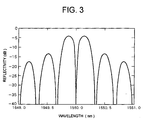
- the reflection spectrum of a grating having such a ⁇ /4-phase-shifted structure exhibits a region where the reflectivity abruptly drops at the Bragg wavelength.
- the uniform Bragg gratings UBG(1) 21, UBG(2) 22 are first-order gratings
- a ⁇ /4-phase-shift corresponds to ⁇ /2 (where ⁇ represents the grating period).
- the gratings are not limited to the first-order gratings but may be constituted as higher-order gratings.
- the first and second uniform gratings UBG(1) 21, UBG(2) 22 have a sinusoidal profile of refractive index as shown in Fig. 2.
- the refractive index profile is not necessarily sinusoidal.
- the UBG(1) 21 and UBG(2) 22 are required to have a refractive index which changes at a fixed period and to serve as Bragg gratings. For example, they may have a rectangular profile, a triangular profile or the like of refractive index distribution.
- a carrier suppressed RZ (CS-RZ) signal using the aforementioned phase-shifted grating (PSBG) 20 When an RZ optical pulse train of the same carrier wavelength as the Bragg wavelength of the PSBG 20 is input into the PSBG 20, a carrier component of the optical pulse train transmits through the PSBG 20, so that the carrier component is not included in a reflected wave.
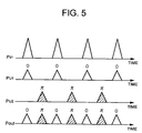
- the input optical pulse train (Pin) is partially reflected by the UBG(1) 21, and the reflected optical pulse train (P U1 ) is guided in the direction opposite to the input optical pulse train Pin.
- a portion of the input optical pulse train Pin which transmits through the UBG(1) 21 is reflected by the UBG(2) 22.
- the reflected optical pulse train (P U2 ) is guided in the same direction as the reflected light pulse train P U1 .
- the reflected optical pulse train P U2 from the UBG(2) 22 experiences a phase difference and a propagation delay with respect to the reflected optical pulse train P U1 from the UBG(1) 21.
- the reflected optical pulse train PU2 has a round-trip phase shift of ⁇ when it is guided to and reflected from the UBG(2) 22.
- the propagation delay time can be adjusted in accordance with the interval between the respective reflection center positions of the UBG(1) 21 and UBG(2) 22, or in accordance with the lengths of the UBG(1) 21 and UBG(2) 22.
- the reflected optical pulse train(Pout) from the ⁇ /4-phase-shifted grating PSBG 20 is a combination of the reflected optical pulse train P U1 from the UBG(1) 21 and the reflected optical pulse train P U2 reflected from the UBG(2) 22 through the phase shift section PS 23 and again passing through the phase shift section PS 23 .
- the optical pulse train Pout has a bit-rate twice as high as that of the input optical pulse train Pin, and has optical pulses which are alternately shifted in phase by ⁇ .
- the reflected optical pulse train Pout from the PSBG 20 can be used as the carrier suppressed RZ(CS-RZ) optical signal.
- Fig. 6 schematically shows the relation in the light intensity between the input optical pulses Pin and the reflected optical pulses from the UBG(1) and UBG(2), when the optical pulse Pin (at wavelength ⁇ C in a vacuum) is input to the phase-shifted fiber grating 10.
- the reflectivity R of the uniform Bragg grating is determined by such parameters as a grating length L, the wavelength ⁇ of light, a detuning amount ⁇ between the Bragg wavelength ⁇ B and the input light wavelength, and a coupling coefficient ⁇ of the light with the grating.
- the wavelength ⁇ is equal to the Bragg grating center wavelength (i.e., when the detuning amount ⁇ is equal to zero)
- the wavelength ⁇ C (wavelength in a vacuum) of the input optical pulse train Pin is chosen to be 1550 nanometers (nm), and the Bragg wavelengths ⁇ B of the UBG(1) 21 and UBG(2) 22 are also chosen to be 1550 nm.
- the optical pulse period is 50 picoseconds (ps)
- the optical pulse width is 25 ps.
- the effective refractive index neff of the fiber including the phase shift section PS 23 is chosen to be 1.45, and the length of the phase shift section PS 23 to be 267.2 nm.
- a delay time of the reflected optical pulses from the UBG(2) 22 is determined by the interval between the reflection center positions of the respective UBG(1) 21 and UBG(2) 22.
- the lengths L U1 , L U2 of the UBG(1) 21 and UBG(2) 22 are chosen to be 2.5 millimeters (mm) (see Fig. 2), respectively, and the interval between the reflection center positions to be 2.5 mm.
- the length L U1, L U2 are approximately equal to the optical path length corresponding to the full width (25 ps) of the optical pulse.
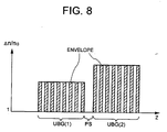
- Fig. 8 shows an envelope of a refractive index modulation factor ⁇ n/n 0 (n 0 represents the refractive index of an optical fiber portion where no grating is formed) in the axial direction of the phase-shifted fiber grating 10. Since the aforementioned coupling coefficient K changes in accordance with the refractive index modulation factor, the reflectivities of the UBG(1) 21 and UBG(2) 22 can be changed.
- the UBG(1) 21 and UBG(2) 22 are gratings which are not apodized (non-apodized gratings).
- the reflected optical pulses P U1 , P U2 from the UBG(1) 21 and UBG(2) 22 have light intensities expressed by R1. (1-R1) 2 R2, respectively, when the light intensity of the input optical pulses Pin is normalized to one, and the reflectivities of the UBG(1) 21 and UBG(2) 22 for the input optical pulses Pin are represented by R1, R2, respectively (see Fig. 6).
- the reflected optical pulse trains P U1 , P U2 are made equal in light intensity by choosing the lengths L U1, L U2 to be equal and providing the UBG(1) 21 and UBG(2) 22 with different refractive index modulation factors.
- the reflected optical pulse train P U2 (broken line) from the UBG(2) 22 deviates in phase from the reflected optical pulse train P U1 (one-dot chain line) from the UBG(1) 21 by ⁇ , while the reflected optical pulse trains are approximately equal in light intensity.
- the interval between respective optical pulses is substantially constant (25 ps).
- the pulse widths of optical pulses in the reflected optical pulse trains P U1 , P U2 are increased by reflection, and partially overlap each other.
- the optical pulse train Pout is a carrier suppressed RZ(CS-RZ) optical signal which has a bit-rate (40 Gbit/s) twice as high as that of the input optical pulse train Pin.
- the UBG(1) 21 and UBG(2) 22 are designed to have different reflectivities R1, R2 to make the light intensities of the reflected optical pulses P U1, P U2 to be equal.
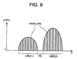
- Fig. 9 schematically illustrates an envelope of a refractive index modulation factor of a ⁇ /4 phase-shifted grating PSBG 20 according to a second embodiment of the present invention.
- an uniform grating UBG(1) 21 has a refractive index modulation factor reduced at both ends in the longitudinal direction of an optical fiber 11.
- UBG(1) 21 is configured as an apodized grating.
- the uniform grating UBG(2) 22 is configured as an apodized grating.
- the apodized gratings result in an improvement in time-axis broadening of reflected pulses by the gratings.
- the uniform grating UBG(1) 21, UBG(2) 22 are not apodized, adjacent optical pulses cancel out each other because the pulses are in an inverted phase relation as shown in Fig. 7B. However, the optical power is lost.
- the uniform gratings UBG(1) 21 and UBG(2) 22 are both apodized to prevent the power loss.
- the uniform gratings UBG(1) 21 and UBG(2) 22 are both apodized, but either one of the gratings may be apodized.
- the overlapping of optical pulses can be reduced by decreasing the full optical pulse width of the input optical pulse train Pin to be one half of the pulse period or less, or by decreasing the full width at half maximum (FWHM) of the optical pulses to be one quarter of the pulse period or less.
- FWHM full width at half maximum
- a phase-shifted grating operates as a wavelength selection Fabry-Perot resonator
- multiple reflections may occur.
- Fig. 10 illustrates multiple reflections by the UBG( 1) 21 and UBG(2) 22 for the input optical pulse train Pin.
- Fig. 11 illustrates interference of optical pulses due to the multiple reflections.
- the multiple reflections for the optical pulse train Pin result in reflected optical pulse trains S1, S2, S3, S4, ....
- a multiple-reflection optical pulse train P-1' comprised of multiple reflection optical pulses S1-1; S2-1, S3-1, S4-1, .... is produced for the first optical pulse P-1 of the optical pulse train Pin, as shown in Fig. 11.
- a multiple-reflection optical pulse train P-2' comprised of multiple reflection optical pulses S1-2, S2-2, S3-2, S4-2, ... is produced for the second optical pulse P-2 of the optical pulse train Pin.
- multiple-reflection optical pulses are produced for the respective optical pulses P-3, P-4 .... of the optical pulse train Pin.
- the coherent cross-talk increases as the reflectivities of the UBG(1) 21 and UBG(2) 22 increases. Therefore, the reflectivities of the UBG(1) 21 and UBG(2) 22 are determined to prevent the coherent cross-talk from affecting the transmission characteristic. For example, in order to limit a power penalty to 1 dB or less after transmission, the reflectivities R1, R2 of the UBG(1) 21 and UBG(2) 22 may be determined to satisfy that the ratio of the intensity of an interfering signal to the intensity of a main signal is equal to or less than -30 dB, i.e., so as to satisfy the following equation: R1xR2 ⁇ 10 -3
- a grating device can be provided for generating a carrier suppressed optical pulse signal having a high transmission performance by forming the phase-shifted grating PSBG 20 so as to satisfy the condition.
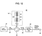
- Fig. 12 is a block diagram showing the configuration of a carrier-suppressed optical carrier signal (CS-RZ signal) generator 30 of a fourth embodiment of the present invention to which the ⁇ / 4-phase-shifted grating PSBG 20 is applied.
- CS-RZ signal carrier-suppressed optical carrier signal
- a light source 31 generates an optical pulse train (RZ signal) having a predetermined pulse period.
- the light source 31 employs, for example, a mode lock laser or the like for generating an RZ optical signal which has a wavelength ⁇ C of 1550 nm (wavelength in a vacuum), an optical pulse width (FWHM) of 12.5 ps, and a bit-rate equal to 20 Gbit/s.
- the generated RZ optical signal is supplied to a first port of an optical circulator 33 through an optical fiber 32.
- the RZ optical signal is output from a second port of the optical circulator 33, and supplied to a ⁇ /4-phase-shifted fiber grating 10.
- the UBG(1) 21 and UBG(2) 22 have the Bragg wavelength ⁇ B of 1550 nm, and a length of 2.5 mm.
- the phase shift section PS 23 has the length of 267.2 nm.
- a CS-RZ optical signal at 40 Gbit/s is produced as a reflected optical pulse train from the phase-shifted fiber grating 10.
- the CS-RZ optical signal is supplied to an optical amplifier (OA) 35 for amplification through the optical circulator 33.
- the optical amplifier (OA) 35 can be implemented by an optical fiber amplifier such as an Erbium-doped fiber amplifier, or a variety of optical amplifiers such as a semiconductor amplifier.
- the CS-RZ optical signal amplified to a predetermined signal level by the optical amplifier (OA) 35 is output from an output terminal 36.
- the CS-RZ optical signal is used as a carrier suppressed optical signal.
- a plurality of CS-RZ signal generators 30 having different wavelengths may be provided to serve as carrier light sources for WDM.
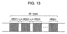
- ⁇ /4-phase-shifted grating 20 comprised of the two uniform gratings UBG(1) 21 and UBG(2) 22, the present invention is not limited to this particular configuration.
- ⁇ /4-phase-shifted grating may be configured so as to include a plurality of uniform gratings UBG(1), UBG(2), ..., UBG(n).
- the plurality of uniform pitch grating waveguides and ⁇ /4-phase-shift waveguides are optically coupled in an alternating sequence.
- the plurality of uniform gratings UBG(1), UBG(2), ..., UBG(n) are sequentially coupled via ⁇ /4-phase-shift sections or waveguides, in which each of the ⁇ /4-phase-shift waveguides is provided between the adjacent uniform gratings, so as to form a multiple ⁇ /4-phase-shift grating waveguide.
- the Bragg wavelengths of the plurality of uniform pitch gratings may be determined such that each of the plurality of uniform pitch gratings reflects the input optical pulses.
- phase-shifted grating (PSBG) waveguide is not necessary configured as an optical fiber grating.
- the phase-shifted grating waveguide may be configured to be planar channel optical waveguide or planar lightwave circuit (PLC).
- a propagation delay time or a pulse interval of the reflected pulse train from the UBG(2) 22 can be adjusted in accordance with the interval between the reflection center positions of the respective UBG(1) 21 and UBG(2) 22.
- the reflectivity of the grating is increased as the product (KL) of the grating length L and coupling coefficient K is increased
- the reflectivity of the UBG(2) 22 can be increased, for example, by forming the grating UBG(2) 22 at the latter stage longer than the grating UBG(1) 21 provided nearer to the light input end.
- the reflectivities of the UBG(1) 21 and UBG(2) 22 can be adjusted without varying the coupling coefficients K, or the refractive index modulation factors thereof. Therefore, the UBG(1) 21 and UBG( 2 ) 22 may be designed to have the same coupling coefficient or refractive index modulation factor.
- the UBG(1) 21 and UBG(2) 22 may be designed to have different refractive index modulation factors and different grating lengths.
- the length of the grating UBG(2) 22 provided at the latter stage may be made shorter than that of the grating UBG(1) 21 provided nearer to the light input end to prevent deterioration of the pulse waveform.
- the present invention is not limited to the wavelength band.
- the present invention can be applied as well to any wavelength band, for example, a 1310 nm band and the like.
- a high-performance, low manufacturing cost grating device which has a reduced insertion loss as well as a simple configuration, and a method and apparatus for generating a train of carrier suppressed pulses.
- a method for generating an optical pulse train includes generating a source optical pulse train having a predetermined pulse period; optically combining a plurality of uniform pitch grating waveguides having a substantially identical Bragg wavelength and ⁇ /4-phase-shift waveguides in an alternating sequence so as to form a multiple ⁇ /4-phase-shift grating waveguide; inputting the source optical pulse train from one end of the multiple ⁇ /4-phase-shifted grating waveguide; and extracting reflected optical pulses by the plurality of uniform pitch grating waveguides from the one end of the multiple ⁇ /4-phase-shifted grating waveguide.
Landscapes
- Physics & Mathematics (AREA)
- Engineering & Computer Science (AREA)
- Microelectronics & Electronic Packaging (AREA)
- Optics & Photonics (AREA)
- General Physics & Mathematics (AREA)
- Computer Networks & Wireless Communication (AREA)
- Signal Processing (AREA)
- Electromagnetism (AREA)
- Optical Communication System (AREA)
- Diffracting Gratings Or Hologram Optical Elements (AREA)
- Lasers (AREA)
- Optical Fibers, Optical Fiber Cores, And Optical Fiber Bundles (AREA)
- Optical Integrated Circuits (AREA)
Applications Claiming Priority (2)
| Application Number | Priority Date | Filing Date | Title |
|---|---|---|---|
| JP2002051307 | 2002-02-27 | ||
| JP2002051307A JP4053787B2 (ja) | 2002-02-27 | 2002-02-27 | 搬送波抑圧光パルス列生成方法及び装置並びにグレーティング装置 |
Publications (3)
| Publication Number | Publication Date |
|---|---|
| EP1341012A2 true EP1341012A2 (de) | 2003-09-03 |
| EP1341012A3 EP1341012A3 (de) | 2005-09-07 |
| EP1341012B1 EP1341012B1 (de) | 2006-09-13 |
Family
ID=27678510
Family Applications (1)
| Application Number | Title | Priority Date | Filing Date |
|---|---|---|---|
| EP03003695A Expired - Lifetime EP1341012B1 (de) | 2002-02-27 | 2003-02-18 | Verfahren und Vorrichtung zur Erzeugung eines optischen Pulszugs mit unterdrücktem Träger und Gitter-Vorrichtung |
Country Status (5)
| Country | Link |
|---|---|
| US (1) | US7039260B2 (de) |
| EP (1) | EP1341012B1 (de) |
| JP (1) | JP4053787B2 (de) |
| KR (1) | KR100858853B1 (de) |
| DE (1) | DE60308244T2 (de) |
Cited By (4)
| Publication number | Priority date | Publication date | Assignee | Title |
|---|---|---|---|---|
| KR100858853B1 (ko) * | 2002-02-27 | 2008-09-17 | 오끼 덴끼 고오교 가부시끼가이샤 | 반송파 억압 광 펄스열 생성 방법 및 장치 그리고 그레이팅 장치 |
| WO2015195016A1 (en) * | 2014-06-19 | 2015-12-23 | Telefonaktiebolaget L M Ericsson (Publ) | An optical device, an optical transceiver and a network node |
| US20210318488A1 (en) * | 2018-06-26 | 2021-10-14 | National Research Council Of Canada | Phase-shifted fiber bragg grating sensor and method for producing same |
| US12613372B2 (en) | 2020-12-04 | 2026-04-28 | National Research Council Of Canada | Low scattering loss high temperature stable fiber Bragg grating sensor based on micropore formation and method for producing same |
Families Citing this family (13)
| Publication number | Priority date | Publication date | Assignee | Title |
|---|---|---|---|---|
| KR100536906B1 (ko) * | 2003-03-19 | 2005-12-16 | 한국전자통신연구원 | 씨에스-알젯 광신호 발생장치 |
| CN100418276C (zh) * | 2004-05-28 | 2008-09-10 | 清华大学 | 分布反馈式光波导激光器 |
| JP4784096B2 (ja) * | 2005-01-12 | 2011-09-28 | 沖電気工業株式会社 | 光パルス時間拡散器及び光符号分割多重伝送装置 |
| WO2007004338A1 (ja) * | 2005-07-01 | 2007-01-11 | University Of Yamanashi | 光信号からクロック信号を抽出する方法および装置 |
| KR100703629B1 (ko) * | 2005-11-30 | 2007-04-06 | 광주과학기술원 | 광 차동 위상 편이 신호 복조기 |
| KR100752362B1 (ko) * | 2005-11-30 | 2007-08-27 | 광주과학기술원 | 위상 가변 기능을 갖는 광 시간 지연 간섭계 |
| JP4876688B2 (ja) * | 2006-04-20 | 2012-02-15 | 沖電気工業株式会社 | 光パルス時間拡散器 |
| JP5184167B2 (ja) * | 2008-03-24 | 2013-04-17 | 古河電気工業株式会社 | リング型レーザ装置 |
| CN101614879B (zh) * | 2009-07-24 | 2011-01-26 | 北京工业大学 | 窄带光滤波器 |
| CN104081694B (zh) * | 2012-02-07 | 2016-08-24 | 瑞典爱立信有限公司 | 光子rf发生器 |
| JP6273701B2 (ja) * | 2013-06-27 | 2018-02-07 | 住友電気工業株式会社 | 光半導体素子 |
| US11125935B2 (en) * | 2019-03-11 | 2021-09-21 | Honeywell International Inc. | Optical structure for imparting a distributed phase shift to an optical signal, electro-optic modulator incorporating such structure for reduced size, low signal loss, and high extinction ratio, and related system and method |
| CN111208689B (zh) * | 2020-01-21 | 2026-03-06 | 天津理工大学 | 双幅度粒子布居数光栅生成方法 |
Family Cites Families (15)
| Publication number | Priority date | Publication date | Assignee | Title |
|---|---|---|---|---|
| US3970959A (en) * | 1973-04-30 | 1976-07-20 | The Regents Of The University Of California | Two dimensional distributed feedback devices and lasers |
| US5361130A (en) | 1992-11-04 | 1994-11-01 | The United States Of America As Represented By The Secretary Of The Navy | Fiber grating-based sensing system with interferometric wavelength-shift detection |
| AUPM386794A0 (en) | 1994-02-14 | 1994-03-10 | University Of Sydney, The | Optical grating |
| US5647039A (en) * | 1995-12-14 | 1997-07-08 | Lucent Technologies Inc. | Optical switching system and devices using a long period grating |
| US6041070A (en) * | 1997-11-14 | 2000-03-21 | Sdl, Inc. | Resonant pumped short cavity fiber laser |
| US5982963A (en) | 1997-12-15 | 1999-11-09 | University Of Southern California | Tunable nonlinearly chirped grating |
| US6046841A (en) | 1998-04-24 | 2000-04-04 | Mahgerefteh; Daniel | All-optical wavelength conversion system comprising an optical discriminator |
| US5974209A (en) | 1998-04-30 | 1999-10-26 | Cho; Pak Shing | System comprising an electroabsorption modulator and an optical discriminator |
| US6292282B1 (en) * | 1998-08-10 | 2001-09-18 | Templex Technology, Inc. | Time-wavelength multiple access optical communication systems and methods |
| KR20000040493A (ko) * | 1998-12-18 | 2000-07-05 | 이계철 | 파장분할다중 광통신 시스템에서의 커플러형 추가/추출 필터 |
| WO2000043828A1 (en) * | 1999-01-26 | 2000-07-27 | Templex Technology, Inc. | Dynamically reconfigurable composite grating filters for temporal waveform processing |
| US6804471B1 (en) | 2000-01-05 | 2004-10-12 | Hrl Laboratories Llc | Apparatus and method of pulsed frequency modulation for analog optical communication |
| US6885686B2 (en) * | 2002-01-18 | 2005-04-26 | Wisconsin Alumni Research Foundation | High coherent power, two-dimensional surface-emitting semiconductor diode array laser |
| JP4053787B2 (ja) * | 2002-02-27 | 2008-02-27 | 沖電気工業株式会社 | 搬送波抑圧光パルス列生成方法及び装置並びにグレーティング装置 |
| US6813447B2 (en) * | 2002-05-23 | 2004-11-02 | Corning Incorporated | Recovery of clock pulses of wavelength division multiplexed optical signals |
-
2002
- 2002-02-27 JP JP2002051307A patent/JP4053787B2/ja not_active Expired - Fee Related
- 2002-12-31 KR KR1020020087837A patent/KR100858853B1/ko not_active Expired - Fee Related
-
2003
- 2003-02-05 US US10/358,316 patent/US7039260B2/en not_active Expired - Fee Related
- 2003-02-18 EP EP03003695A patent/EP1341012B1/de not_active Expired - Lifetime
- 2003-02-18 DE DE60308244T patent/DE60308244T2/de not_active Expired - Lifetime
Cited By (6)
| Publication number | Priority date | Publication date | Assignee | Title |
|---|---|---|---|---|
| KR100858853B1 (ko) * | 2002-02-27 | 2008-09-17 | 오끼 덴끼 고오교 가부시끼가이샤 | 반송파 억압 광 펄스열 생성 방법 및 장치 그리고 그레이팅 장치 |
| WO2015195016A1 (en) * | 2014-06-19 | 2015-12-23 | Telefonaktiebolaget L M Ericsson (Publ) | An optical device, an optical transceiver and a network node |
| US9876578B2 (en) | 2014-06-19 | 2018-01-23 | Telefonaktiebolaget Lm Ericsson (Publ) | Optical device, an optical transceiver and a network node |
| US20210318488A1 (en) * | 2018-06-26 | 2021-10-14 | National Research Council Of Canada | Phase-shifted fiber bragg grating sensor and method for producing same |
| EP3814815A4 (de) * | 2018-06-26 | 2022-04-06 | National Research Council of Canada | Phasenverschobener faser-bragg-gitter-sensor und verfahren zu seiner herstellung |
| US12613372B2 (en) | 2020-12-04 | 2026-04-28 | National Research Council Of Canada | Low scattering loss high temperature stable fiber Bragg grating sensor based on micropore formation and method for producing same |
Also Published As
| Publication number | Publication date |
|---|---|
| US20030161581A1 (en) | 2003-08-28 |
| DE60308244T2 (de) | 2007-03-29 |
| JP2003258344A (ja) | 2003-09-12 |
| KR100858853B1 (ko) | 2008-09-17 |
| JP4053787B2 (ja) | 2008-02-27 |
| EP1341012A3 (de) | 2005-09-07 |
| DE60308244D1 (de) | 2006-10-26 |
| US7039260B2 (en) | 2006-05-02 |
| EP1341012B1 (de) | 2006-09-13 |
| KR20030071479A (ko) | 2003-09-03 |
Similar Documents
| Publication | Publication Date | Title |
|---|---|---|
| EP1341012B1 (de) | Verfahren und Vorrichtung zur Erzeugung eines optischen Pulszugs mit unterdrücktem Träger und Gitter-Vorrichtung | |
| US7174103B2 (en) | Optical signal converter, optical encoder, optical decoder, and optical code division multiplexing communication apparatus | |
| Giles | Lightwave applications of fiber Bragg gratings | |
| US6628864B2 (en) | Optical code generation and detection | |
| US7027468B2 (en) | Phase-insensitive recovery of clock pulses of wavelength division multiplexed optical signals | |
| US20080285977A1 (en) | Method and apparatus for transmitting optical signals | |
| EP1227363B1 (de) | Nichtlinearer optischer Ringspiegel | |
| EP0892516A2 (de) | Gesamt-optische Zeitdemultiplex-Schaltung und gesamtoptische TDM-WDM Konversionsschaltung | |
| Chen et al. | Applications of ultrashort pulse propagation in Bragg gratings for wavelength-division multiplexing and code-division multiple access | |
| JP6653886B2 (ja) | モード合分波器及びモード多重伝送システム | |
| Willner et al. | Fixed and tunable management of fiber chromatic dispersion | |
| Chan et al. | Widely tunable, high-FSR, coherence-free microwave photonic notch filter | |
| EP1460783B1 (de) | Wellenlängenvariable Raman-Pumpquelle zur optischen breitbandigen Verstärkung | |
| US5864421A (en) | Optical frequency shifter and optical soliton-like return-to-zero pulse transmission system using optical frequency shifter | |
| US7034988B2 (en) | Wavelength conversion device | |
| Li et al. | A dual-wavelength and dual-repetition-rate actively mode-locked fiber ring laser | |
| Petruzzi et al. | Dispersion compensation using only fiber Bragg gratings | |
| JP4140390B2 (ja) | 光符号化信号生成装置及び光符号分割多重装置 | |
| KR100438014B1 (ko) | 다중 모드 간섭을 이용한 가변 광필터 | |
| JP2004070166A (ja) | 光フィルタ | |
| US7031580B2 (en) | Restoring optical pulses | |
| EP1436920B1 (de) | Optisches übertragungssystem mit dispersionsverwaltungssystem | |
| Teh | Applications of superstructure fibre Bragg gratings for optical code division multiple access and packet switched networks | |
| Turitsyna | Advanced fibre Bragg gratings: design and applications | |
| Dalotra et al. | Performance Analysis of Nonlinearities in Optical Fibers |
Legal Events
| Date | Code | Title | Description |
|---|---|---|---|
| PUAI | Public reference made under article 153(3) epc to a published international application that has entered the european phase |
Free format text: ORIGINAL CODE: 0009012 |
|
| AK | Designated contracting states |
Kind code of ref document: A2 Designated state(s): AT BE BG CH CY CZ DE DK EE ES FI FR GB GR HU IE IT LI LU MC NL PT SE SI SK TR |
|
| AX | Request for extension of the european patent |
Extension state: AL LT LV MK RO |
|
| PUAL | Search report despatched |
Free format text: ORIGINAL CODE: 0009013 |
|
| AK | Designated contracting states |
Kind code of ref document: A3 Designated state(s): AT BE BG CH CY CZ DE DK EE ES FI FR GB GR HU IE IT LI LU MC NL PT SE SI SK TR |
|
| AX | Request for extension of the european patent |
Extension state: AL LT LV MK RO |
|
| RIC1 | Information provided on ipc code assigned before grant |
Ipc: 7H 04B 10/155 B Ipc: 7G 02B 6/293 A Ipc: 7H 01S 3/13 B |
|
| GRAP | Despatch of communication of intention to grant a patent |
Free format text: ORIGINAL CODE: EPIDOSNIGR1 |
|
| 17P | Request for examination filed |
Effective date: 20060206 |
|
| AKX | Designation fees paid |
Designated state(s): DE FR GB |
|
| GRAS | Grant fee paid |
Free format text: ORIGINAL CODE: EPIDOSNIGR3 |
|
| GRAA | (expected) grant |
Free format text: ORIGINAL CODE: 0009210 |
|
| AK | Designated contracting states |
Kind code of ref document: B1 Designated state(s): DE FR GB |
|
| REG | Reference to a national code |
Ref country code: GB Ref legal event code: FG4D |
|
| REF | Corresponds to: |
Ref document number: 60308244 Country of ref document: DE Date of ref document: 20061026 Kind code of ref document: P |
|
| ET | Fr: translation filed | ||
| PLBE | No opposition filed within time limit |
Free format text: ORIGINAL CODE: 0009261 |
|
| STAA | Information on the status of an ep patent application or granted ep patent |
Free format text: STATUS: NO OPPOSITION FILED WITHIN TIME LIMIT |
|
| 26N | No opposition filed |
Effective date: 20070614 |
|
| PGFP | Annual fee paid to national office [announced via postgrant information from national office to epo] |
Ref country code: FR Payment date: 20100223 Year of fee payment: 8 |
|
| PGFP | Annual fee paid to national office [announced via postgrant information from national office to epo] |
Ref country code: DE Payment date: 20100226 Year of fee payment: 8 Ref country code: GB Payment date: 20100202 Year of fee payment: 8 |
|
| GBPC | Gb: european patent ceased through non-payment of renewal fee |
Effective date: 20110218 |
|
| REG | Reference to a national code |
Ref country code: FR Ref legal event code: ST Effective date: 20111102 |
|
| REG | Reference to a national code |
Ref country code: DE Ref legal event code: R119 Ref document number: 60308244 Country of ref document: DE Effective date: 20110901 |
|
| PG25 | Lapsed in a contracting state [announced via postgrant information from national office to epo] |
Ref country code: FR Free format text: LAPSE BECAUSE OF NON-PAYMENT OF DUE FEES Effective date: 20110228 |
|
| PG25 | Lapsed in a contracting state [announced via postgrant information from national office to epo] |
Ref country code: GB Free format text: LAPSE BECAUSE OF NON-PAYMENT OF DUE FEES Effective date: 20110218 |
|
| PG25 | Lapsed in a contracting state [announced via postgrant information from national office to epo] |
Ref country code: DE Free format text: LAPSE BECAUSE OF NON-PAYMENT OF DUE FEES Effective date: 20110901 |