EP1341308A1 - Phasenregelschleife - Google Patents
Phasenregelschleife Download PDFInfo
- Publication number
- EP1341308A1 EP1341308A1 EP02256718A EP02256718A EP1341308A1 EP 1341308 A1 EP1341308 A1 EP 1341308A1 EP 02256718 A EP02256718 A EP 02256718A EP 02256718 A EP02256718 A EP 02256718A EP 1341308 A1 EP1341308 A1 EP 1341308A1
- Authority
- EP
- European Patent Office
- Prior art keywords
- switch
- output
- phase
- charge pump
- loop
- Prior art date
- Legal status (The legal status is an assumption and is not a legal conclusion. Google has not performed a legal analysis and makes no representation as to the accuracy of the status listed.)
- Granted
Links
Images




Classifications
-
- H—ELECTRICITY
- H03—ELECTRONIC CIRCUITRY
- H03L—AUTOMATIC CONTROL, STARTING, SYNCHRONISATION OR STABILISATION OF GENERATORS OF ELECTRONIC OSCILLATIONS OR PULSES
- H03L7/00—Automatic control of frequency or phase; Synchronisation
- H03L7/06—Automatic control of frequency or phase; Synchronisation using a reference signal applied to a frequency- or phase-locked loop
- H03L7/08—Details of the phase-locked loop
- H03L7/085—Details of the phase-locked loop concerning mainly the frequency- or phase-detection arrangement including the filtering or amplification of its output signal
- H03L7/089—Details of the phase-locked loop concerning mainly the frequency- or phase-detection arrangement including the filtering or amplification of its output signal the phase or frequency detector generating up-down pulses
- H03L7/0891—Details of the phase-locked loop concerning mainly the frequency- or phase-detection arrangement including the filtering or amplification of its output signal the phase or frequency detector generating up-down pulses the up-down pulses controlling source and sink current generators, e.g. a charge pump
- H03L7/0895—Details of the current generators
-
- H—ELECTRICITY
- H03—ELECTRONIC CIRCUITRY
- H03L—AUTOMATIC CONTROL, STARTING, SYNCHRONISATION OR STABILISATION OF GENERATORS OF ELECTRONIC OSCILLATIONS OR PULSES
- H03L7/00—Automatic control of frequency or phase; Synchronisation
- H03L7/06—Automatic control of frequency or phase; Synchronisation using a reference signal applied to a frequency- or phase-locked loop
- H03L7/08—Details of the phase-locked loop
- H03L7/14—Details of the phase-locked loop for assuring constant frequency when supply or correction voltages fail
-
- H—ELECTRICITY
- H03—ELECTRONIC CIRCUITRY
- H03L—AUTOMATIC CONTROL, STARTING, SYNCHRONISATION OR STABILISATION OF GENERATORS OF ELECTRONIC OSCILLATIONS OR PULSES
- H03L7/00—Automatic control of frequency or phase; Synchronisation
- H03L7/06—Automatic control of frequency or phase; Synchronisation using a reference signal applied to a frequency- or phase-locked loop
- H03L7/16—Indirect frequency synthesis, i.e. generating a desired one of a number of predetermined frequencies using a frequency- or phase-locked loop
- H03L7/18—Indirect frequency synthesis, i.e. generating a desired one of a number of predetermined frequencies using a frequency- or phase-locked loop using a frequency divider or counter in the loop
Definitions
- the present invention relates to a phase-locked loop, and more particularly to an improved phase-locked loop used as a local oscillator in a radio communication system, which is capable of maintaining the control voltage of the voltage controlled oscillator (VCO) constant during the open-loop operation, while coping with the tendency of reducing a source voltage.
- VCO voltage controlled oscillator
- Phase-locked loops are used as local oscillators in various communication systems.
- a PLL is incorporated in a front-end transceiver of a radio communication system to synchronize a local oscillation signal with an externally supplied reference signal.
- FIG. 1A illustrates a conventional PLL 100 used as a local oscillator in a radio communication system.
- PLL 100 comprises a phase detector 110, a charge pump 120, a loop filter 130, a voltage controlled oscillator (VCO) 140, and a programmable divider 150, in which an output from the VCO 140 is fed back to the phase detector 110 to define a closed loop.
- the phase detector 110 compares the phase of the feedback clock supplied from the VCO 140 with a reference clock externally supplied, and outputs a signal in proportion to the phase difference.
- the charge pump 120 and the loop filter 130 extract a low-frequency component (i.e., a differential component) from the output signal of the phase detector 110, and supply the extracted low-frequency component to the VCO 140.
- the VCO 140 varies its oscillating frequency based on the output from the loop filter 130.
- the PLL used in a radio communication system has an FSK (frequency shift keying) modulating function, in addition to the above-described local oscillating function.
- FSK modulation is a function for shifting the output frequency between two or more prescribed values in accordance with, for example, multiple channels.
- the output frequency is locked to a carrier frequency under the closed loop, and then, the loop of the PLL 100 is opened.
- a modulation signal is applied directly to the voltage controlled oscillator (VCO 140) from an external circuit (such as a baseband processing circuit connected to the front-end transceiver) to generate frequency-shifted waves.
- VCO 140 voltage controlled oscillator
- a PLL ordinarily operates in the closed-loop mode, functioning as a feedback circuit; however, it works in the open-loop mode when carrying out, for example, FSK modulation.
- the simplest way for opening the loop of the PLL 100 is turning off the charge pump 120.
- FIG. 1B illustrates a conventional charge pump 120 used in the PLL 100.
- the charge pump 120 can be realized as a simple structure shown in FIG. 1B through a CMOS process.
- the charge pump 120 comprises a switch (PMOS transistor M3) 123 that is turned on by application of an up signal, and a switch (NMOS transistor M4) 124 that is turned on by application of a down signal.
- a feedback signal input to the terminal fp of the phase detector 110 is compared with a reference signal input to the terminal fr. If the phase of the reference signal is ahead of that of the feedback signal, the phase detector 110 outputs a zero voltage or a negative voltage (which is referred to as "LOW") from its output terminal pu, which causes the PMOS transistor (M3) 123 of the charge pump 120 to be turned on. Upon turning on the PMOS transistor (M3) 123, charge is accumulated in the capacitor of the loop filter 130. Assuming that the control characteristic of the VCO 140 (FIG. 1A) has a positive polarity, the control voltage of the VCO 140 increases in accordance with the accumulation of charge in the loop filter 130.
- the phase of the feed back signal becomes into consistent with that of the reference signal.
- the phase of the reference signal input to the terminal fr is behind the feedback signal
- LOW is output from the terminal pd to turn on the NMOS transistor (M4) 124 of the charge pump 120. Then, the charge is taken out of the loop filter 130, and the control voltage of the VCO 140 lowers. As a result, the output frequency of the VCO 140 decreases, and the phase of the feedback signal becomes into consistent with that of the reference signal.
- the charge pump 120 is turned off. Both PMOS transistor 123 and NMOS transistor 124 of the charge pump 120 are turned off forcibly by an external control signal, regardless of the output of the phase detector 110. In the off state of the transistors 123 and 124, charge does not flow in and out of the capacitor of the loop filter 130. Consequently, the control voltage of the VCO 140 is maintained constant, and the output frequency of the VCO 140 becomes constant.
- a modulation signal is applied directly to the input terminal vc of the VCO 140 from an adder of the external circuit (e.g., the baseband processing circuit).
- the output frequency of the VCO 140 changes in response to the change in the voltage level of the VCO 140, and a prescribed value of FSK modulation waves can be obtained.
- the current becomes unbalanced.
- a current supply is used, or alternatively, the switches are differentiated to increase the speed of response of the charge pump 120.
- the design rule of the CMOS process becomes finer and finer, and the power source voltage is lowered along with the continued miniaturization of the circuit design.
- the threshold voltage is set lower, off-leakage of the MOS transistor becomes large. For example, when PMOS transistor 123 and NMOS transistor 124 are turned off in the charge pump 120 shown in FIG. 1B to open the loop, the charge accumulated in the capacity of the loop filter 130 fluctuates due to off-leakage of the transistors 123 and 124, and consequently, the control voltage of the VCO 140 abruptly varies.
- FIG. 2 illustrates a simulation result of the voltage drift of the loop filter due to off-leakage that occurs when PMOS transistor 123 and NMOS transistor 124 are turned off in the conventional charge pump 120 of the PLL 100.
- the amount of voltage change increases, and the voltage varies by 0.15V or more in 100 ⁇ s. This phenomenon prevents the PLL 100 from maintaining the transmission frequency constant under the open loop, and FSK modulation can not be carried out appropriately.
- transistors with a relatively long channel-length may be used to reduce the off-leakage from PMOS transistor (M3) and NMOS transistor (M4).
- M3 and M4 that are connected to the output of the charge pump 120 becomes large, and another problem arises, that is, the speed of response of the charge pump 120 slows down.
- the present invention was conceived to overcome the above-described problems in the prior art, and it is an object of the invention to provide a phase-locked loop that can maintain the control voltage of the voltage control oscillator (VCO) constant under the open loop, while coping with the trend of reducing the power source voltage along with the miniaturization of the CMOS process.
- VCO voltage control oscillator
- a third switch is inserted before the output of the charge pump to control switching between the open loop and the closed loop of the PLL.
- the third switch can be realized as, for example, a MOS transistor.
- a phase-locked loop comprises a phase detector receiving an externally supplied reference clock and a feedback clock; a charge pump connected to the output of the phase detector; a loop filter extracting a low-frequency component from the output of the charge pump; and a voltage controlled oscillator (VCO) having an input connected to the output of the loop filter and an output connected to the feedback clock supplied to the phase detector, in which the charge pump comprises a first switch that controls outputting a negative current based on the output of the phase detector, a second switch that controls outputting a positive current based on the output of the phase detector, a third switch connected between the first switch and the second switch to control an output to the loop filter, and an input terminal receiving a switching control signal for controlling opening and closing of the third switch.
- VCO voltage controlled oscillator
- a long-channel transistor with little leakage current can be used as the third switch, while using high-speed short-channel transistors for the first and second switches. Consequently, the leakage current flowing during the open-loop operation can be reduced, without deteriorating the speed of response, and the control voltage of the voltage controlled oscillator (VCO) can be maintained constant.
- VCO voltage controlled oscillator
- the input terminal receiving the switching control signal is connected directly to the third switch to control the opening and closing of the loop, regardless with the ON/OFF states of the first and second switches. This arrangement can reduce undesirable off-leakage, without slowing down the speed of response.
- the charge pump further comprises a control circuit connected before the first and second switches to control the ON/OFF operations of the first, second, and third switches.
- the input terminal for receiving the switching control signal is connected to the control circuit.
- the control circuit controls the first, second, and third switches so that the third switch is turned off, while turning on the first and second switches.
- FIG. 3 illustrates, in a block diagram, a phase-locked loop (PLL) 1 according to the invention
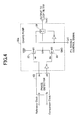
- FIG. 4 illustrates an example of the charge pump 20a used in the phase-locked loop (PLL) 1 shown in FIG. 3 according to the first embodiment of the invention.
- the phase-locked loop (PLL) 1 comprises a phase detector 10, a charge pump 20 connected to the phase detector 10, a loop filter 30 connected to the charge pump 20, and a voltage controlled oscillator (VCO) 40 connected to the loop filter 30.
- the output of the voltage controlled oscillator (VCO) 40 is fed back to the phase detector 10 to define a loop.
- the charge pump 20 has an input terminal that receives a switching control signal "enable" for controlling opening and closing the loop.
- the input terminal fr of the phase detector 10 receives a reference clock, which is externally supplied and used in the PLL 1, while the input terminal fp receives an output of the VCO 40, or its frequency-divided signal, which is to be compared with the reference clock.
- the phase detector 10 has a known structure shown in FIG. 5. If the phase of the feedback clock (or the comparison clock) supplied from the VCO 40 is behind that of the reference clock, an up signal is output from the output terminal pu of the phase detector 10 in order to raise the control voltage of the VCO 40 to increase the output frequency.
- phase of the feedback clock supplied from the VCO 40 is ahead of that of the reference clock, then a down signal is output from the output terminal pd of the phase detector 10 in order to reduce control voltage of the VCO 40 to decrease the output frequency.
- the charge pump 20a has a first MOS transistor (M1) 22 receiving the up signal at its gate, a second MOS transistor (M2) 23 receiving the inversion of the output from the terminal pd of the phase detector at its gate, and a third switch 24 connected to the drain voltage V1 of the first and second MOS transistors 22 and 23.
- the MOS transistor (M1) 22 functions as a first switch for controlling outputting a positive current
- the MOS transistor (M2) 23 functions as a second switch for controlling outputting a negative current.
- an input terminal (ct) receiving a PLL enable signal is connected directly to the third switch 24 to control the opening and closing of the loop of the PLL 1.
- the PLL enable signal is applied to the gate of the third switch 24.
- a low level (Low) representing logical "0" is input, as the PLL enable control signal, to the input terminal (ct). Then, the third switch 23 is turned on, which causes the PLL to operate in the ordinary closed loop.
- a high level (Hi) representing logical "1" is input, as the PLL enable control signal, to the input terminal (ct) to turn off the third switch 24. Since the third switch 24 is connected to the loop filter 30, the charge accumulated in the loop filter 30 does not change as long as the third switch is turned off. Consequently, the control voltage of the VCO 40 can be maintained constant during the open-loop operation.
- FIG. 6 is a diagram illustrating the first switch (PMOS transistor M1) 22, the second switch (NMOS transistor M2) 23, and the third switch 24 of the charge pump 20a as a resistor circuit.
- the resistances of the first, second and third switches 22, 23, 24 are denoted as R1, R2 and R3, and electric currents flowing through R1, R2 and R3 are denoted as I1, I2 and I3.
- I3 electric current flowing through the third switch 24 is expressed by equation (1).
- electric current I3 expressed by equation (1) which is generated in the charge pump of the first embodiment shown in FIG. 4, is much smaller than the electric current I3 of the conventional charge pump expressed by equation (2) because R1, R2, and R3 take positive values.
- the PLL 1 can maintain the transmission frequency stably during the open-loop operation.
- FIG. 7 illustrates a charge pump 20b used in the PLL 1 according to the second embodiment of the invention.
- the charge pump 20b comprises a first transistor (M1) 26 that controls outputting a positive current, a second transistor (M2) 27 that controls outputting a negative current, a third switch 28 connected to the drain voltage V1 of the first and second transistors 26 and 27, and a control circuit 25 that controls the ON/OFF operations of the first transistor (M1) 26, the second transistor (M2) 27, and the third switch 28.
- the input terminal (ct) receiving a PLL enable control signal is connected to the control circuit 25, and the opening and closing of the third switch 28 is controlled by the control circuit 25.
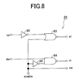
- FIG. 8 illustrates an example of the control circuit 25 shown in FIG. 7.
- the control circuit 25 illustrated in FIG. 8 comprises an inverting element 65 connected to the output terminal pu of the phase detector 10, a NOR gate 63 receiving the output of the inverting element 65 and the PLL enable control signal, an inverting element 66 receiving the PLL enable signal, and a NAND gate 64 receiving the output of the inverting element 66 and the down signal from the output terminal pd of the phase detector 10.
- the NAND gate 64 outputs logical "1" when at least one of the inputs is logical "0", and therefore, "Hi" is applied to the gate of the NMOS transistor (i.e., the second transistor M2) 27 via the node ni of the control circuit 25. Consequently, the second transistor 27 is also turned on.
- Electric current I3 flowing through the third switch 28 is expressed by equation (1), as has been described in the first embodiment.
- the ON/OFF operation of the third switch 24 is controlled independently, and accordingly, the first transistor (M1) 22 and the second transistor (M2) 23 are in the OFF state most of the time during the open-loop operation.
- I 3 1 1 2 ⁇ ( R off + R 3) ⁇ VDD where R off denotes the off resistance of the first and second transistors 22 and 23.
- equation (3) can be approximated to equation (5).
- I 3 2 a 2 2 ⁇ (2+ a 2) ⁇ R 3 .
- VDD where a2 denotes a value of coeffieicent "a" when the first transistor 26 and the second transistor 27 are both in the ON state in the second embodiment.
- the condition that satisfies I3 2 ⁇ I3 1 is R off ⁇ 2 a 2 ⁇ R3 .
- R off is the off resistance of the first transistor (M1) 22 and the second transistor (M2) 23 in the structure of the first embodiment
- R3 is the off resistance of the third switch 28 of the second embodiment. Since the third switch 28 can be realized as a long-channel transistor, R3 is equal to or greater than R off .
- a2 represents the difference in ON resistance between the first transistor (M1) 26 and the second transistor (M2) 27, a2 is smaller than 1 (a2 ⁇ 1). Accordingly, condition of inequality (6) is satisfied.
- I3 2 appearing at the output of the charge pump 20b of the second embodiment is smaller than I3 1 appearing at the output of the charge pump 20a of the first embodiment, and that the influence on the loop filter 30 can be further reduced. Even if a charge pump with a low threshold voltage is used in the PLL 1, the control voltage of the voltage controlled oscillator (VCO) 40 is maintained constant in a stable manner during the open-loop operation.
- VCO voltage controlled oscillator
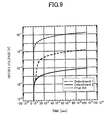
- FIG. 9 is a graph showing the effect of the present invention for reducing the voltage drift of the PLL 1, where the horizontal axis represents time and the vertical axis represents the time-variable offset voltage expressed in logarithmic form.
- the dashed line indicates the offset voltage of the conventional charge pump
- the long dashed line indicates the offset voltage of the PLL of the first embodiment
- the solid line indicates the offset voltage of the PLL of the second embodiment.
- the offset voltage greatly increases as time passes due to the difference in off-leakage between the first (PMOS) transistor M3 and the second (NMOS) transistor M4.
- using the charge pump according to the first embodiment can reduce the voltage fluctuation by order of magnitude two, as compared with the conventional circuit.
- the structure of the second embodiment can further reduce the voltage fluctuation by order of magnitude two, as compared with the circuit of the first embodiment.
- the present invention realizes a phase-locked loop (PLL) that is capable of efficiently reducing the leakage current from the charge pump during the open-loop operation, even if the charge pump is comprised of CMOS transistors which are likely to produce more leakage current as the CMOS process becomes finer, and as the threshold voltage is set lower.
- PLL phase-locked loop
- control circuit used in the second embodiment to control opening and closing the loop is realized by a combination of the NOR gate and the NAD gate.
- control circuitry that can turn on the first and second transistors during the open-loop operation may be employed as the control circuit.
Landscapes
- Stabilization Of Oscillater, Synchronisation, Frequency Synthesizers (AREA)
Applications Claiming Priority (2)
| Application Number | Priority Date | Filing Date | Title |
|---|---|---|---|
| JP2002030565A JP3748414B2 (ja) | 2002-02-07 | 2002-02-07 | 位相同期ループ回路 |
| JP2002030565 | 2002-02-07 |
Publications (2)
| Publication Number | Publication Date |
|---|---|
| EP1341308A1 true EP1341308A1 (de) | 2003-09-03 |
| EP1341308B1 EP1341308B1 (de) | 2005-10-26 |
Family
ID=27654749
Family Applications (1)
| Application Number | Title | Priority Date | Filing Date |
|---|---|---|---|
| EP02256718A Expired - Lifetime EP1341308B1 (de) | 2002-02-07 | 2002-09-26 | Phasenregelschleife |
Country Status (4)
| Country | Link |
|---|---|
| US (1) | US6759912B2 (de) |
| EP (1) | EP1341308B1 (de) |
| JP (1) | JP3748414B2 (de) |
| DE (1) | DE60206875T2 (de) |
Families Citing this family (11)
| Publication number | Priority date | Publication date | Assignee | Title |
|---|---|---|---|---|
| JP4546716B2 (ja) * | 2003-11-10 | 2010-09-15 | シャープ株式会社 | Pllクロック信号生成回路 |
| EP1564890A1 (de) * | 2004-02-13 | 2005-08-17 | Ecole Polytechnique Federale De Lausanne | Analoges selbstkalibrierendes Verfahren und Vorrichtung für einen rauscharmen, schnellen und breitbandigen Phasenregelkreis |
| JP4371893B2 (ja) * | 2004-04-27 | 2009-11-25 | セイコーNpc株式会社 | チャージポンプ回路及びこのチャージポンプ回路を用いたpll回路 |
| US7102400B1 (en) * | 2004-08-30 | 2006-09-05 | Sitel Semiconductor B.V. | Phase locked loop charge pump and method of operation |
| FR2879858B1 (fr) * | 2004-12-16 | 2007-03-30 | St Microelectronics Sa | Procede de correction du dephasage entre deux signaux d'enree d'une boucle a verrouillage de phase et dispositif associe |
| KR100660638B1 (ko) * | 2005-10-26 | 2006-12-21 | 삼성전자주식회사 | 고전압 발생 회로 및 이를 구비하는 반도체 장치 |
| US20090039929A1 (en) * | 2007-08-06 | 2009-02-12 | International Business Machines Corporation | Method to Reduce Static Phase Errors and Reference Spurs in Charge Pumps |
| US9000836B2 (en) | 2008-01-10 | 2015-04-07 | Micron Technology, Inc. | Voltage generator circuit |
| DE102008035456B4 (de) * | 2008-07-30 | 2012-09-06 | Lantiq Deutschland Gmbh | Schaltungsanordnung und Verfahren zur Erzeugung eines Signals mit im Wesentlichen konstantem Signalpegel |
| CN102136840B (zh) * | 2011-04-22 | 2016-03-16 | 上海华虹宏力半导体制造有限公司 | 自偏置锁相环 |
| CN103036411B (zh) * | 2012-11-30 | 2017-03-08 | 上海华虹宏力半导体制造有限公司 | 电荷泵电路 |
Citations (4)
| Publication number | Priority date | Publication date | Assignee | Title |
|---|---|---|---|---|
| EP0376847A2 (de) * | 1988-12-28 | 1990-07-04 | Fujitsu Limited | PLL-Synthetisierer |
| US5675292A (en) * | 1996-06-05 | 1997-10-07 | Mccune, Jr.; Earl W. | Phase lock loop enabling smooth loop bandwidth switching over a wide range |
| EP0840456A2 (de) * | 1990-10-22 | 1998-05-06 | NEC Corporation | Frequenzsynthetisierer mit PLL, der einen Frequenzwechsel des Ausgangs mit hoher Geschwindigkeit ermöglicht |
| EP1006662A2 (de) * | 1998-12-04 | 2000-06-07 | Fujitsu Limited | Integrierte Halbleiterschaltung |
Family Cites Families (4)
| Publication number | Priority date | Publication date | Assignee | Title |
|---|---|---|---|---|
| US5847614A (en) * | 1996-11-15 | 1998-12-08 | Analog Devices, Inc. | Low power charge pump |
| JP3851511B2 (ja) * | 2001-03-14 | 2006-11-29 | 株式会社ルネサステクノロジ | Fm送信機 |
| US6580329B2 (en) * | 2001-04-11 | 2003-06-17 | Tropian, Inc. | PLL bandwidth switching |
| JP3808338B2 (ja) * | 2001-08-30 | 2006-08-09 | 株式会社ルネサステクノロジ | 位相同期回路 |
-
2002
- 2002-02-07 JP JP2002030565A patent/JP3748414B2/ja not_active Expired - Lifetime
- 2002-09-26 US US10/254,973 patent/US6759912B2/en not_active Expired - Fee Related
- 2002-09-26 DE DE60206875T patent/DE60206875T2/de not_active Expired - Lifetime
- 2002-09-26 EP EP02256718A patent/EP1341308B1/de not_active Expired - Lifetime
Patent Citations (4)
| Publication number | Priority date | Publication date | Assignee | Title |
|---|---|---|---|---|
| EP0376847A2 (de) * | 1988-12-28 | 1990-07-04 | Fujitsu Limited | PLL-Synthetisierer |
| EP0840456A2 (de) * | 1990-10-22 | 1998-05-06 | NEC Corporation | Frequenzsynthetisierer mit PLL, der einen Frequenzwechsel des Ausgangs mit hoher Geschwindigkeit ermöglicht |
| US5675292A (en) * | 1996-06-05 | 1997-10-07 | Mccune, Jr.; Earl W. | Phase lock loop enabling smooth loop bandwidth switching over a wide range |
| EP1006662A2 (de) * | 1998-12-04 | 2000-06-07 | Fujitsu Limited | Integrierte Halbleiterschaltung |
Also Published As
| Publication number | Publication date |
|---|---|
| DE60206875T2 (de) | 2006-05-24 |
| US6759912B2 (en) | 2004-07-06 |
| DE60206875D1 (de) | 2005-12-01 |
| EP1341308B1 (de) | 2005-10-26 |
| US20030146794A1 (en) | 2003-08-07 |
| JP2003234651A (ja) | 2003-08-22 |
| JP3748414B2 (ja) | 2006-02-22 |
Similar Documents
| Publication | Publication Date | Title |
|---|---|---|
| JP3250540B2 (ja) | Pll回路 | |
| JP2845185B2 (ja) | Pll回路 | |
| US5825640A (en) | Charge pump circuit and method | |
| US8330511B2 (en) | PLL charge pump with reduced coupling to bias nodes | |
| EP1341308B1 (de) | Phasenregelschleife | |
| US5285114A (en) | Phase lock loop charge pump with symmetrical charge and discharge currents | |
| US9490824B1 (en) | Phase-locked loop with frequency bounding circuit | |
| US20080136531A1 (en) | Adaptive bandwidth phase locked loop with feedforward divider | |
| KR20100094859A (ko) | 비대칭 전하 펌프 및 그것을 포함한 위상 동기 루프 | |
| US7719331B2 (en) | PLL circuit | |
| US9407137B2 (en) | Charge pump circuit and PLL circuit | |
| US9401699B2 (en) | High frequency low-gain noise ring-type VCO oscillator leading to a low-noise/area PLL | |
| US7835220B2 (en) | PLL circuit for increasing potential difference between ground voltage and reference voltage or power source voltage of oscillation circuit | |
| US8022740B2 (en) | Fast-response phase-locked loop charge-pump driven by low voltage input | |
| EP0545517A1 (de) | Rauscharme Lade-Entladungsschaltung mit Multiplexbetriebenen Tore | |
| KR100711103B1 (ko) | 적응형 3상태 위상 주파수 검출기 및 검출방법과 이를이용한 위상동기루프 | |
| US7576578B2 (en) | Frequency synthesizer and charge pump circuit used for the same | |
| US20030142774A1 (en) | Half-rate clock and data recovery circuit | |
| US7504891B1 (en) | Initialization circuit for a phase-locked loop | |
| US6864723B2 (en) | High-swing transconductance amplifier | |
| US6236843B1 (en) | Radio terminal device for automatically correcting phase difference between a received signal and an internally generated signal | |
| US7944257B2 (en) | Method and system of optimizing a control system using low voltage and high-speed switching | |
| US20030214330A1 (en) | Phase-locked loop circuit | |
| US6628153B2 (en) | PLL circuit and frequency division method reducing spurious noise | |
| JP2003298414A (ja) | 半導体集積回路 |
Legal Events
| Date | Code | Title | Description |
|---|---|---|---|
| PUAI | Public reference made under article 153(3) epc to a published international application that has entered the european phase |
Free format text: ORIGINAL CODE: 0009012 |
|
| 17P | Request for examination filed |
Effective date: 20021010 |
|
| AK | Designated contracting states |
Kind code of ref document: A1 Designated state(s): AT BE BG CH CY CZ DE DK EE ES FI FR GB GR IE IT LI LU MC NL PT SE SK TR |
|
| AX | Request for extension of the european patent |
Extension state: AL LT LV MK RO SI |
|
| AKX | Designation fees paid |
Designated state(s): DE FR GB |
|
| 17Q | First examination report despatched |
Effective date: 20040511 |
|
| GRAP | Despatch of communication of intention to grant a patent |
Free format text: ORIGINAL CODE: EPIDOSNIGR1 |
|
| GRAS | Grant fee paid |
Free format text: ORIGINAL CODE: EPIDOSNIGR3 |
|
| GRAA | (expected) grant |
Free format text: ORIGINAL CODE: 0009210 |
|
| AK | Designated contracting states |
Kind code of ref document: B1 Designated state(s): DE FR GB |
|
| REG | Reference to a national code |
Ref country code: GB Ref legal event code: FG4D |
|
| REF | Corresponds to: |
Ref document number: 60206875 Country of ref document: DE Date of ref document: 20051201 Kind code of ref document: P |
|
| ET | Fr: translation filed | ||
| PLBE | No opposition filed within time limit |
Free format text: ORIGINAL CODE: 0009261 |
|
| STAA | Information on the status of an ep patent application or granted ep patent |
Free format text: STATUS: NO OPPOSITION FILED WITHIN TIME LIMIT |
|
| 26N | No opposition filed |
Effective date: 20060727 |
|
| PGFP | Annual fee paid to national office [announced via postgrant information from national office to epo] |
Ref country code: DE Payment date: 20140912 Year of fee payment: 13 |
|
| PGFP | Annual fee paid to national office [announced via postgrant information from national office to epo] |
Ref country code: FR Payment date: 20140806 Year of fee payment: 13 Ref country code: GB Payment date: 20140806 Year of fee payment: 13 |
|
| REG | Reference to a national code |
Ref country code: DE Ref legal event code: R119 Ref document number: 60206875 Country of ref document: DE |
|
| GBPC | Gb: european patent ceased through non-payment of renewal fee |
Effective date: 20150926 |
|
| REG | Reference to a national code |
Ref country code: FR Ref legal event code: ST Effective date: 20160531 |
|
| PG25 | Lapsed in a contracting state [announced via postgrant information from national office to epo] |
Ref country code: DE Free format text: LAPSE BECAUSE OF NON-PAYMENT OF DUE FEES Effective date: 20160401 Ref country code: GB Free format text: LAPSE BECAUSE OF NON-PAYMENT OF DUE FEES Effective date: 20150926 |
|
| PG25 | Lapsed in a contracting state [announced via postgrant information from national office to epo] |
Ref country code: FR Free format text: LAPSE BECAUSE OF NON-PAYMENT OF DUE FEES Effective date: 20150930 |