EP1345311A2 - Entladungslampenreaktanz mit hohem Leistungsfaktor - Google Patents
Entladungslampenreaktanz mit hohem Leistungsfaktor Download PDFInfo
- Publication number
- EP1345311A2 EP1345311A2 EP03005300A EP03005300A EP1345311A2 EP 1345311 A2 EP1345311 A2 EP 1345311A2 EP 03005300 A EP03005300 A EP 03005300A EP 03005300 A EP03005300 A EP 03005300A EP 1345311 A2 EP1345311 A2 EP 1345311A2
- Authority
- EP
- European Patent Office
- Prior art keywords
- output
- rectifier
- circuit
- accordance
- lamp
- Prior art date
- Legal status (The legal status is an assumption and is not a legal conclusion. Google has not performed a legal analysis and makes no representation as to the accuracy of the status listed.)
- Withdrawn
Links
Images
Classifications
-
- H—ELECTRICITY
- H05—ELECTRIC TECHNIQUES NOT OTHERWISE PROVIDED FOR
- H05B—ELECTRIC HEATING; ELECTRIC LIGHT SOURCES NOT OTHERWISE PROVIDED FOR; CIRCUIT ARRANGEMENTS FOR ELECTRIC LIGHT SOURCES, IN GENERAL
- H05B41/00—Circuit arrangements or apparatus for igniting or operating discharge lamps
- H05B41/14—Circuit arrangements
- H05B41/26—Circuit arrangements in which the lamp is fed by power derived from DC by means of a converter, e.g. by high-voltage DC
- H05B41/28—Circuit arrangements in which the lamp is fed by power derived from DC by means of a converter, e.g. by high-voltage DC using static converters
- H05B41/282—Circuit arrangements in which the lamp is fed by power derived from DC by means of a converter, e.g. by high-voltage DC using static converters with semiconductor devices
- H05B41/2825—Circuit arrangements in which the lamp is fed by power derived from DC by means of a converter, e.g. by high-voltage DC using static converters with semiconductor devices by means of a bridge converter in the final stage
- H05B41/2828—Circuit arrangements in which the lamp is fed by power derived from DC by means of a converter, e.g. by high-voltage DC using static converters with semiconductor devices by means of a bridge converter in the final stage using control circuits for the switching elements
-
- H—ELECTRICITY
- H05—ELECTRIC TECHNIQUES NOT OTHERWISE PROVIDED FOR
- H05B—ELECTRIC HEATING; ELECTRIC LIGHT SOURCES NOT OTHERWISE PROVIDED FOR; CIRCUIT ARRANGEMENTS FOR ELECTRIC LIGHT SOURCES, IN GENERAL
- H05B41/00—Circuit arrangements or apparatus for igniting or operating discharge lamps
- H05B41/14—Circuit arrangements
- H05B41/26—Circuit arrangements in which the lamp is fed by power derived from DC by means of a converter, e.g. by high-voltage DC
- H05B41/28—Circuit arrangements in which the lamp is fed by power derived from DC by means of a converter, e.g. by high-voltage DC using static converters
Definitions
- the present invention relates to a compact electronic circuit or ballast for powering from the mains discharge lamps such as fluorescent lamps with a power factor near unity and a limited lamp current crest factor.
- Electronic ballasts are devices for powering high frequency (on the order of tens of kHz) discharge lamps with indubitable advantages in terms of efficiency and performance such as absence of flicker, protectors et cetera.
- a half-bridge converter or inverter commuting an almost continuous voltage at the desired frequency is typically used. Starting from the mains it is therefore first of all necessary to rectify the sinusoidal voltage to 50Hz. The most economical way to do this is to use a diode bridge (whole wave or double half-wave rectifier) followed by a filtering capacitor of appropriate value (typically on the order of tens of ⁇ F) to reduce the residual ripple to 100Hz.
- a diode bridge whole wave or double half-wave rectifier
- a filtering capacitor of appropriate value typically on the order of tens of ⁇ F
- This simple circuit suffers from the disadvantage of causing absorption of current from the mains with a trend very far from the ideal sinusoidal wave form. Indeed, the diode bridge conducts for a small period of time for each hemicycle giving origin to absorption of a pulsed current from the mains with resulting high harmonic distortion. In addition, there is a high lamp current crest factor.
- an active stage for active correction of the power factor can be used.
- a switching power supply supplying an adjusted direct voltage to ensure an approximately sinusoidal wave form of the current absorbed from the mains and easily obtaining a power factor near unity.
- This circuit completely resolves the problem of limitation of harmonic currents and also allows obtaining excellent lamp current crest factors.
- the main disadvantages are cost and the large number of added components required, to wit, the controller (typically an 8-pin integrated circuit), a power MOSFet, a transformer and numerous passive surrounding components.
- Another disadvantage is the need for a larger mains filter because of the noise introduced by the MOSFet switching.
- the general purpose of the present invention is to remedy the above mentioned shortcomings by making available an electronic reactor circuit for discharge lamps which would be simple, economical and strong and would provide satisfactory limitation of the harmonic content of the current absorbed from the mains with a good lamp current crest factor and limited voltage at the ends of the bulk capacitance.
- an electronic device for powering a fluorescent lamp from a sinusoidal alternating voltage source comprising a whole bridge rectifier which would rectify said alternating voltage, a rectified voltage processing circuit connected in parallel to the rectifier output, a half-bridge inverter with an output for high frequency powering of the lamp starting from a direct voltage output of said processing circuit obtained by means of a bulk capacitor connected in parallel to the output of the rectifier through a first diode characterized in that there is a resonant network comprising the lamp which is connected between the output of the half-bridge inverter and an intermediate point of a series of two capacitors connected in parallel to the rectifier output.
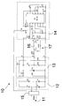
- FIG. 10 shows the electrical diagram of an innovative electronic device or ballast designated as a whole by reference number 10 for powering a discharge lamp 16 and in particular a fluorescent lamp from a source of sinusoidal alternating voltage applied to the input terminals 11.
- Said source is generally the normal electrical power distribution mains.
- the circuit comprises a whole-bridge diode rectifier 12 which rectifies the alternating voltage applied to the input 11.
- the rectified voltage output from the bridge 12 is applied to a circuit 13 connected in parallel to the output of the rectifier 12.
- the circuit 13 supplies a direct voltage output (terminals A-C) which is converted by a generically known half-bridge inverter 14 for high frequency powering of the lamp 16, and a point B for connection of one end of a resonant network 17 consisting of the series of an inductance LRES and a capacitor CRES and comprising the lamp 16 connected in parallel to the resonance capacitance CRES.
- the other end of the resonant network 17 is connected to the output D of the inverter.
- the inverter 14 has the half bridge made up of a pair of power MOSFets Q1, Q2 controlled by a half-bridge pilot circuit comprising a specialized integrated circuit IC1 with its own network of accompanying components (D5-D7, C1-C5, R1-R3).
- the diagram of the inverter 14 using by way of example the known integrated circuit IR2156 produced by International Rectifier is of a known type and not further described (any half bridge driver can be used). It supplies to its own output D a square wave with 50% duty cycle and frequency at least above 10kHz (advantageously around 40kHz).
- the resistance R3 connected between the pins 2,3 of the integrated circuit and the anode of the diode D1 ensures powering of the integrated circuit during startup.
- the half-bridge driver starts to oscillate, the power supply of the integrated circuit is ensured by the charge pump consisting of the capacitor C1 and the diodes D5 and D7.
- the circuit 13 supplies the virtually direct voltage to points A-C by means of a bulk capacitor CB connected in parallel to the output of the rectifier 12 through a first diode DP.
- Point B is obtained as the intermediate point of a series of two capacitors CP1, CP2 connected in parallel to the output of the rectifier 12.
- the circuit 13 comprises a second diode DC2 connected to the cathode at the intermediate point B and with the anode to the negative pole C of the direct voltage output A-C and a third diode DC1 connected to the anode again at the intermediate point B and to the cathode at the positive pole A of the direct voltage output A-C.
- the two diodes DC1 and DC2 have the function of containing the range of the voltage at the ends of the resonant network of the load so as to keep the lamp current crest factor limited.
- the input diode bridge 12 leads practically for the entire half-wave through a charge pump circuit consisting in the complete circuit shown of the capacitances CP1, CP2, CP3 and the diodes DP, DC1 and DC2.
- the voltage VB must be greater than the rectified input voltage; this way the bridge diode and the diode DP cannot be polarized directly simultaneously, i.e. they cannot both conduct at the same time.
- the input line current is thus equal to the charge current of the capacitance CP1 combined with the current running in CP3 with each switching cycle of the half bridge (on the order of tens of microseconds).
- the diodes D1, D2, D3 and D4 of the input rectifier bridge 12 are thus run through by a high frequency current and will therefore have to be fast diodes (fast switching rectifiers).
- This current is of course proportionate to the input voltage at each switching cycle of the inverter; its mean value thus has a sinusoidal behavior. This reduces harmonic distortion to the minimum.
- a known simple antistatic filter 15 can be fitted at the input of the rectifier 12 so as to curb the reduced EMI noise which might be generated.
- Sizing of the various components is closely tied to the nature of the load it is desired to power and in particular to its electrical parameters, to wit, nominal power, current and voltage.
- the inductance LRES is on the order of mH while the capacitance CRES is measured in tens of nF.
- the capacitances CP2 and CP3 must be of the same order of magnitude of CRES while CP1 is on the order of hundreds of nF.
- the voltage at the ends of the bulk capacitor - typically an electrolyte with capacitance on the order of tens of microfarads - is little more than 400V in order to be able to use capacitors with nominal voltage of 450V which are readily available on the market.
- Performance obtained is extremely interesting and especially allows respecting the standard, to wit, power factor over 0.97 and harmonic content (up to the thirty-ninth harmonic) well below the limits set in EN-61000-3-2.
- the stability of the inverter supply voltage it can be held at a value sufficient to allow direct lighting of the lamp without the interposition of step-up transformers with the resulting cost and space savings.
Landscapes
- Circuit Arrangements For Discharge Lamps (AREA)
Applications Claiming Priority (2)
| Application Number | Priority Date | Filing Date | Title |
|---|---|---|---|
| ITMI20020564 | 2002-03-15 | ||
| IT2002MI000564A ITMI20020564A1 (it) | 2002-03-15 | 2002-03-15 | Reattore elettronico ad alto fattoe di potenza per lampade a scarica |
Publications (2)
| Publication Number | Publication Date |
|---|---|
| EP1345311A2 true EP1345311A2 (de) | 2003-09-17 |
| EP1345311A3 EP1345311A3 (de) | 2005-04-13 |
Family
ID=11449528
Family Applications (1)
| Application Number | Title | Priority Date | Filing Date |
|---|---|---|---|
| EP03005300A Withdrawn EP1345311A3 (de) | 2002-03-15 | 2003-03-11 | Entladungslampenreaktanz mit hohem Leistungsfaktor |
Country Status (2)
| Country | Link |
|---|---|
| EP (1) | EP1345311A3 (de) |
| IT (1) | ITMI20020564A1 (de) |
Cited By (2)
| Publication number | Priority date | Publication date | Assignee | Title |
|---|---|---|---|---|
| EP2104402A1 (de) * | 2008-03-17 | 2009-09-23 | Chuan Shih Industrial Co., Ldt. | Elektronisches Vorschaltgerät für Gasentladungslampen |
| GB2464497A (en) * | 2008-10-17 | 2010-04-21 | Kaoyi Electronic Co Ltd | Fluorescent light electronic ballast circuit |
Families Citing this family (1)
| Publication number | Priority date | Publication date | Assignee | Title |
|---|---|---|---|---|
| CN104282209A (zh) * | 2014-10-24 | 2015-01-14 | 吴筱枝 | 一种电学演示教具 |
Family Cites Families (7)
| Publication number | Priority date | Publication date | Assignee | Title |
|---|---|---|---|---|
| US6057652A (en) * | 1995-09-25 | 2000-05-02 | Matsushita Electric Works, Ltd. | Power supply for supplying AC output power |
| CN1113583C (zh) * | 1996-09-24 | 2003-07-02 | 马士科技有限公司 | 荧光灯电子镇流器 |
| US5994847A (en) * | 1997-01-31 | 1999-11-30 | Motorola Inc. | Electronic ballast with lamp current valley-fill power factor correction |
| IL127335A0 (en) * | 1998-11-30 | 1999-09-22 | N L G I Electronics Ltd | Self exciting high freqency converter for gas discharge lamp |
| CN2394401Y (zh) * | 1999-10-25 | 2000-08-30 | 俞志龙 | 低灯电流波峰比的高功率因数电子镇流器 |
| JP2001176689A (ja) * | 1999-12-15 | 2001-06-29 | Si Electronics:Kk | 蛍光灯制御装置 |
| US6356034B1 (en) * | 2000-03-22 | 2002-03-12 | Regal King Manufacturing Limited | Low voltage discharge lamp power supply |
-
2002
- 2002-03-15 IT IT2002MI000564A patent/ITMI20020564A1/it unknown
-
2003
- 2003-03-11 EP EP03005300A patent/EP1345311A3/de not_active Withdrawn
Cited By (3)
| Publication number | Priority date | Publication date | Assignee | Title |
|---|---|---|---|---|
| EP2104402A1 (de) * | 2008-03-17 | 2009-09-23 | Chuan Shih Industrial Co., Ldt. | Elektronisches Vorschaltgerät für Gasentladungslampen |
| GB2464497A (en) * | 2008-10-17 | 2010-04-21 | Kaoyi Electronic Co Ltd | Fluorescent light electronic ballast circuit |
| GB2464497B (en) * | 2008-10-17 | 2013-07-31 | Kaoyi Electronic Co Ltd | Fluorescent light electronic ballast circuit |
Also Published As
| Publication number | Publication date |
|---|---|
| ITMI20020564A0 (it) | 2002-03-15 |
| EP1345311A3 (de) | 2005-04-13 |
| ITMI20020564A1 (it) | 2003-09-15 |
Similar Documents
| Publication | Publication Date | Title |
|---|---|---|
| Poorali et al. | Analysis of the integrated SEPIC-flyback converter as a single-stage single-switch power-factor-correction LED driver | |
| US8368314B2 (en) | Charge pump electronic ballast for use with low input voltage | |
| KR100724155B1 (ko) | 일단형 pfc와 전력 변환기 회로 | |
| EP2124509A2 (de) | Vorschaltgerät für Entladungslampe mit Leistungsfaktorverbesserung | |
| JP2003520407A (ja) | 多ランプ動作用の電力帰還力率修正方式 | |
| US6118225A (en) | High frequency discharge lamp operating circuit with resonant power factor correction circuit | |
| US8427064B2 (en) | Electronic ballast circuit for fluorescent lamps | |
| De Morais et al. | A high power factor ballast using a single switch with both power stages integrated | |
| WO2011086440A2 (en) | A power factor correction circuit of an electronic ballast | |
| Vilela et al. | An electronic ballast with high power factor and low voltage stress | |
| JP2000003798A (ja) | 放電ランプ点灯装置および照明装置 | |
| CN110419157A (zh) | 具有电荷泵电路的驱动器 | |
| CA2549206A1 (en) | Electronic ballast for at least one lamp | |
| EP1345311A2 (de) | Entladungslampenreaktanz mit hohem Leistungsfaktor | |
| Chiu et al. | Single-stage voltage source charge-pump electronic ballast with switched-capacitor dimmer for multiple fluorescent lamps | |
| Cardesín et al. | Low-cost PFC electronic ballast for 250W HID lamps operating as constant power source with 400 kHz switching frequency | |
| WO2010054454A2 (en) | Electronic ballast for metal vapor lamps using integration techniques for power factor correction and acoustic resonance elimination | |
| KR101220255B1 (ko) | 광원들을 동작시키기 위한 회로 어레인지먼트 | |
| Pereira et al. | Electronic ballast for fluorescent lamps with the PFC stage integrated with the resonant inverter | |
| CN103874306A (zh) | 具有无源功率因数校正的电子镇流器 | |
| JP3493943B2 (ja) | 電源装置 | |
| JP3733675B2 (ja) | インバータ装置、放電灯点灯装置及び照明装置 | |
| KR100871109B1 (ko) | 직류교류겸용 고압방전등용 안정기회로 | |
| Morais et al. | An electronic ballast employing a boost half-bridge topology | |
| CN1925710A (zh) | Sepic变换器的电隔离 |
Legal Events
| Date | Code | Title | Description |
|---|---|---|---|
| PUAI | Public reference made under article 153(3) epc to a published international application that has entered the european phase |
Free format text: ORIGINAL CODE: 0009012 |
|
| AK | Designated contracting states |
Kind code of ref document: A2 Designated state(s): AT BE BG CH CY CZ DE DK EE ES FI FR GB GR HU IE IT LI LU MC NL PT SE SI SK TR |
|
| AX | Request for extension of the european patent |
Extension state: AL LT LV MK RO |
|
| PUAL | Search report despatched |
Free format text: ORIGINAL CODE: 0009013 |
|
| AK | Designated contracting states |
Kind code of ref document: A3 Designated state(s): AT BE BG CH CY CZ DE DK EE ES FI FR GB GR HU IE IT LI LU MC NL PT SE SI SK TR |
|
| AX | Request for extension of the european patent |
Extension state: AL LT LV MK RO |
|
| RIC1 | Information provided on ipc code assigned before grant |
Ipc: 7H 05B 41/282 B Ipc: 7H 05B 41/24 A |
|
| 17P | Request for examination filed |
Effective date: 20051010 |
|
| AKX | Designation fees paid |
Designated state(s): AT BE BG CH CY CZ DE DK EE ES FI FR GB GR HU IE IT LI LU MC NL PT RO SE SI SK TR |
|
| 17Q | First examination report despatched |
Effective date: 20060914 |
|
| STAA | Information on the status of an ep patent application or granted ep patent |
Free format text: STATUS: THE APPLICATION IS DEEMED TO BE WITHDRAWN |
|
| 18D | Application deemed to be withdrawn |
Effective date: 20080318 |