EP1346314B1 - Gleichzeitige elektrische personalisierung und graphisches drucken einer chipkarte - Google Patents
Gleichzeitige elektrische personalisierung und graphisches drucken einer chipkarte Download PDFInfo
- Publication number
- EP1346314B1 EP1346314B1 EP01993902A EP01993902A EP1346314B1 EP 1346314 B1 EP1346314 B1 EP 1346314B1 EP 01993902 A EP01993902 A EP 01993902A EP 01993902 A EP01993902 A EP 01993902A EP 1346314 B1 EP1346314 B1 EP 1346314B1
- Authority
- EP
- European Patent Office
- Prior art keywords
- support
- objects
- customization
- face
- graphic printing
- Prior art date
- Legal status (The legal status is an assumption and is not a legal conclusion. Google has not performed a legal analysis and makes no representation as to the accuracy of the status listed.)
- Expired - Lifetime
Links
Images


Classifications
-
- G—PHYSICS
- G06—COMPUTING OR CALCULATING; COUNTING
- G06K—GRAPHICAL DATA READING; PRESENTATION OF DATA; RECORD CARRIERS; HANDLING RECORD CARRIERS
- G06K17/00—Methods or arrangements for effecting co-operative working between equipments covered by two or more of main groups G06K1/00 - G06K15/00, e.g. automatic card files incorporating conveying and reading operations
Definitions
- the field of the invention is that of the manufacture of intelligent portable objects such as smart cards, and more particularly that of their personalization.
- the customization is therefore performed successively first by electrical writing, then the graphic customization is performed.
- data from electrical customization are often used to obtain, by querying a database for example, the graphical data corresponding to the object to be manufactured.
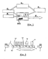
- the different stages of electrical and graphic customization are represented figure 1 .
- the different elements allowing to realize these stages are represented figure 2 .
- the electrical customization time varies in particular depending on the type of chip and the application. As an indication, the average time of electrical customization of a mobile GSM chip is for example about 12 seconds. It is then necessary, to maintain a usual rate of 3600 cards per hour, one card per second, to increase the number of electric personalization heads: twelve (12) in the case of GSM smart cards.
- an object of the invention is to perform electrical and graphical customizations in masked time, on a single equipment.
- Power and graphics customization in one location ensures correlation security of electrical and graphical information and avoids fraud as any attempt to recover card between the two operations does not complete both operations.
- the invention also has the advantage of reducing the number of equipment and its size, since the two equipment of Electrical customization and graphic personalization are replaced by a unique equipment.
- the cards 1 comprising a chip 2 are placed on a support 3.
- This support 3 moves to present the chips 2 to a single or multiple electric personalization station 4 to perform the steps E1 and E2.
- the electrical customization station 4 shown on the figure 2 is a multiple customization station to increase the rate. It has an elevator which groups together several smart cards 1, for example 10 cards, then distributes them in front of as many customization heads before transferring them for the next step.
- the read data are submitted to the processing unit responsible for step E3 and then the bodies of the cards 1 are presented to a graphic personalization station 5 to perform step E4.
- the customization is sequential with two mechanical systems that can possibly be either two devices (one per system), or a device grouping the two systems, each system having a box discarded for cards with defects.
- Electrically but not graphically personalized smart cards are usually white or printed with a generic pattern for all cards; they can not be differentiated from each other in particular by the operator in charge of electrical and graphic personalization. This results in a significant risk of error or fraud when the graphic customization is not carried out on the good map already electrically personalized.
- the printing time Ti is observed, such that: 1s ⁇ Ti ⁇ 15s.
- the electric personalization time varies in particular according to the type of chip and the application as explained above.
- a carrier 3 of the smart cards 1 to be personalized is in the form of a wheel or drum rotatable and having locations for receiving the cards 1, for example 36 smart cards.
- the electrical customization station comprises electrical customization heads 40 distributed and fixed inside the drum 3, vis-à-vis each chip location of the cards 1. As shown figure 4b ), these chip locations are materialized by marks 30 possibly in the form of cavities, formed on the drum 3.
- the stationary graphic printing station consists of one or more print heads 50 depending on whether it is desired to obtain monochrome or color printing.
- the graphic print heads 50 are preferably situated on the other side of the smart card 1 with respect to the electrical personalization heads 40.
- 256-jet inkjet printing heads can be used per head.
- the inks will then be dried by a drying device 51 of the inks, for example an ultraviolet lamp.
- a drying device 51 of the inks for example an ultraviolet lamp.
- Other printing devices may be used, including thermal printing devices.
- This equipment of course comprises input devices 6 and output 7 of the smart cards 1. It furthermore comprises a dimensional control system 8 of smart cards 1 to be personalized, consisting for example of a camera and a control system. graphic control 9 printed smart cards which can also be made of a camera.
- the input device 6 of the smart cards 1 places the cards 1 on the drum 3.
- the drum 1 presents the smart cards 1 to the dimensional control system 8 of the cards, to the print heads 50, to the device drying 51 possibly then to the graphical control system 9.
- the smart cards 1 are in contact with or in relation to the electric personalization heads 40.
- the personalization heads Electrical 40 write or read data inside the chip.
- the chip In the case of contact cards, the chip is flush with the surface of the card.
- the personalization heads 40 then comprise electrical contacts by which the information inside the chip is written and / or read. Since the graphic print heads 50 are located on the other side of the card relative to the electrical customization heads 40, the graphic information is printed on the face of the card opposite to the electrical contacts of the card.
- the contacts of the chip are constituted by an antenna buried in the body of the card.
- the electrical customization heads 40 then comprise antennas by which are written and / or read the information inside the chip.
- the chip has both flush contacts and an antenna.
- the personalization heads 40 then comprise antennas and / or electrical contacts.
- Electrical and graphic personalization can be achieved in a single pass of smart cards under the printing station or in several passes.
- the rotation of the drum makes it possible to carry out several passages, for example 6. This rotation is preferably carried out in one direction but it can be carried out in one and / or the other direction.
- FIG. 5 A second embodiment of an equipment according to the invention is presented figure 5 .
- the support 3 is plane.
- graphic customization may require one or more passes.
- the printing station comprising the print heads 50 can be fixed as in the previous embodiment.
- the support 3 can then be animated by a constant and unique translational movement or back-and-forth depending on whether it is a once-through graphic printing of the smart card 1 or multiple passes. Print times of 4 to 6 seconds can be achieved.
- the printing station can instead be mobile: it is then the print heads 50 that make the passes on the smart cards 1, the support 3 being fixed.
- the printing station can be driven by a constant and unique translational movement or back-and-forth depending on whether it is a single-pass graphic printing of the smart card or multiple passages. The performances obtained are often inferior to those of the previous case.
- electrical and graphic personalization operations are performed automatically without the smart cards being manipulated by an operator and thus ensure the coherence of electrical and graphic information.
- step E3 figures 1 and 3 We also improve the management of electrical or graphic waste. Indeed, if one of the video control systems (8 or 9 systems figure 4a )) or verification of the electrical data (step E3 figures 1 and 3 ) detects that a card 1 is not compliant, the smart card 1 can then have its graphic impression modified to clearly indicate that the smart card 1 is not compliant: a text such as "rejected” or For example, "rejection” can be added. The content of the electrically written information can also be blocked or erased so that the use of the smart card is no longer possible.
Landscapes
- Physics & Mathematics (AREA)
- General Physics & Mathematics (AREA)
- Engineering & Computer Science (AREA)
- Theoretical Computer Science (AREA)
- Credit Cards Or The Like (AREA)
- Die Bonding (AREA)
- Encapsulation Of And Coatings For Semiconductor Or Solid State Devices (AREA)
Claims (9)
- Ausrüstung für die Personalisierung von tragbaren intelligenten Objekten wie Chipkarten (1), wobei die genannten tragbaren Objekte auf einer ersten Seite grafisch und auf einer zweiten Seite elektrisch personalisierbar sind, wobei die genannte Ausrüstung folgendes umfasst:- einen Träger (3), elektrische Personalisierungsmittel (40) dieser Objekte (1);- einen grafischen Druckposten (50) dieser Objekte (1),
dadurch gekennzeichnet, dass sie unter anderem folgendes umfasst:- Verschiebemittel des Trägers (3) in Bezug auf den grafischen Druckposten (50) oder umgekehrt; dass der Träger auf einer ersten seiner Seiten Plätze hat, um die zu personalisierenden Objekte (1) aufzunehmen, und auf der anderen Seite die genannten elektrischen Personalisierungsmittel dieser Objekte, und dass der grafische Druckposten (50) an der Seite der ersten Seite des Trägers und der ersten Seite der zu personalisierenden Objekte angeordnet ist, so dass jedes vom Träger getragene Objekt sich beim Verschieben des Trägers in Bezug auf den grafischen Druckposten oder umgekehrt gleichzeitig zwischen einem der elektrischen Personalisierungsmittel (40) und dem genannten grafischen Druckposten (50) befindet, wobei das elektrische Personalisierungsmittel (40) und der grafische Druckposten (50) mindestens teilweise gleichzeitig auf dieses Objekt einwirken. - Ausrüstung gemäß Anspruch 1, dadurch gekennzeichnet, dass der Träger (3) ortsfest und der grafische Druckposten (5) mobil ist.
- Ausrüstung gemäß Anspruch 1, dadurch gekennzeichnet, dass der Träger (3) mobil und der grafische Druckposten (5) ortsfest ist.
- Ausrüstung gemäß einem der Ansprüche 1 bis 3, dadurch gekennzeichnet, dass der Träger (3) eine Trommel ist, beispielsweise mit etwa horizontaler Rotationsachse.
- Ausrüstung gemäß einem der Ansprüche 1 bis 4, dadurch gekennzeichnet, dass die elektrischen Personalisierungsmittel (40) der Karten elektrische Kontakte umfassen, die mit den Plätzen der Chips (30) der auf dem Träger (3) angeordneten zu personalisierenden Objekte (1) in Kontakt stehen.
- Ausrüstung gemäß einem der Ansprüche 1 bis 5, dadurch gekennzeichnet, dass die elektrischen Personalisierungsmittel (40) der Objekte (1) Antennen umfassen, die gegenüber den Plätzen der Chips (30) der auf dem Träger (3) angeordneten Objekte (1) angebracht sind und die gegenüber dem grafischen Druckposten (50) liegen.
- Ausrüstung gemäß einem der Ansprüche 1 bis 6, dadurch gekennzeichnet, dass sie eine grafische (9) und/oder elektrische Kontrollvorrichtung (8) der zu personalisierenden Objekte (1) und/oder eine Trockenvorrichtung (51) des Drucks umfasst.
- Verfahren für die kontinuierliche Personalisierung von tragbaren intelligenten Objekten wie Chipkarten (1), wobei die genannten tragbaren Objekte auf einer ersten Seite grafisch und auf einer zweiten Seite elektrisch personalisierbar sind, dadurch gekennzeichnet, dass das genannte Verfahren Schritte umfasst, um die zu personalisierenden Objekte an Plätzen anzuordnen, die auf einer ersten Seite eines Trägers vorgesehen sind, so dass jedes tragbare Objekt elektrisch personalisiert werden kann über ein elektrisches Personalisierungsmittel (40), das auf einer zweiten Seite des Trägers angeordnet ist, um dann den Träger gegenüber einen grafischen Druckposten (50) zu verschieben, der an der Seite der ersten Seite des Trägers und der ersten Seite des zu personalisierenden Objekts angeordnet ist; wobei die Verschiebung derart erfolgt, dass sich jedes zu personalisierende Objekt gleichzeitig zwischen einem elektrischen Personalisierungsmittel (40) und dem grafischen Druckposten (50) befindet, so dass das genannte Mittel (40) und der genannte Posten (50) mindestens teilweise gleichzeitig auf das zu personalisierende Objekt einwirken.
- Verfahren gemäß Anspruch 8, dadurch gekennzeichnet, dass die elektrische Personalisierung (40) komplett während des grafischen Drucks (50) erfolgt.
Applications Claiming Priority (3)
| Application Number | Priority Date | Filing Date | Title |
|---|---|---|---|
| FR0014560 | 2000-11-13 | ||
| FR0014560A FR2816738B1 (fr) | 2000-11-13 | 2000-11-13 | Machine et procede de personnalisation de cartes a puces |
| PCT/FR2001/003418 WO2002039375A1 (fr) | 2000-11-13 | 2001-11-06 | Personnalisation electrique et impression graphique d'une carte a puce en temps masque |
Publications (2)
| Publication Number | Publication Date |
|---|---|
| EP1346314A1 EP1346314A1 (de) | 2003-09-24 |
| EP1346314B1 true EP1346314B1 (de) | 2010-04-21 |
Family
ID=8856370
Family Applications (1)
| Application Number | Title | Priority Date | Filing Date |
|---|---|---|---|
| EP01993902A Expired - Lifetime EP1346314B1 (de) | 2000-11-13 | 2001-11-06 | Gleichzeitige elektrische personalisierung und graphisches drucken einer chipkarte |
Country Status (9)
| Country | Link |
|---|---|
| US (1) | US6827264B2 (de) |
| EP (1) | EP1346314B1 (de) |
| CN (1) | CN100498826C (de) |
| AT (1) | ATE465466T1 (de) |
| AU (1) | AU2002223750A1 (de) |
| DE (1) | DE60141914D1 (de) |
| ES (1) | ES2344731T3 (de) |
| FR (1) | FR2816738B1 (de) |
| WO (1) | WO2002039375A1 (de) |
Families Citing this family (14)
| Publication number | Priority date | Publication date | Assignee | Title |
|---|---|---|---|---|
| FR2847363B1 (fr) * | 2002-11-15 | 2005-01-07 | Smartware | Machine a haute cadence de personnalisation de module a circuit integre |
| FR2862409B1 (fr) * | 2003-11-17 | 2006-04-14 | Datacard Inc | Element d'adaptation pour supports electroniques programmables |
| EP1755092A1 (de) * | 2005-08-01 | 2007-02-21 | Axalto SA | Herstellungsmaschine und Verfahren zur Programmierung von tragbaren Geräten |
| US7309007B2 (en) * | 2005-10-04 | 2007-12-18 | First Data Corporation | Systems and methods for personalizing transaction cards |
| BRPI0621206A2 (pt) * | 2006-01-25 | 2011-12-06 | On Track Innovations Ltd | aparelho para processar uma folha de núcleo de documento e processo para processar um engaste de núcleo em uma folha de núcleo |
| US7991692B2 (en) * | 2006-10-09 | 2011-08-02 | First Data Corporation | Electronic payment instrument and packaging |
| FR2918196B1 (fr) * | 2007-06-27 | 2009-08-14 | Datacard Corp | Machine pour personnaliser des cartes a puce avec une cadence elevee. |
| US7885878B2 (en) | 2008-05-28 | 2011-02-08 | First Data Corporation | Systems and methods of payment account activation |
| DE102008051516A1 (de) * | 2008-06-03 | 2009-12-24 | Mühlbauer Ag | Codiervorrichtung für Datenträger und Verfahren zum Codieren von Datenträgern |
| US9306666B1 (en) | 2009-10-08 | 2016-04-05 | Dynamics Inc. | Programming protocols for powered cards and devices |
| FR2953617B1 (fr) * | 2009-12-03 | 2012-01-20 | Herve Mongin | Machine de personnalisation electrique et graphique d'objets electroniques portatifs |
| WO2013177762A1 (en) * | 2012-05-30 | 2013-12-05 | Gemalto Technologies (Shanghai) Co., Ltd. | Smart card graphical and electrical personalization module and method of graphical and electrical personalization for smart cards |
| CN103029451B (zh) * | 2012-12-27 | 2015-02-11 | 广州市华标科技发展有限公司 | 组合式多功能制证设备及方法 |
| EP3383662B1 (de) | 2016-01-08 | 2020-09-02 | Entrust Datacard Corporation | Kartendruckmechanismus kartenrückweg |
Family Cites Families (9)
| Publication number | Priority date | Publication date | Assignee | Title |
|---|---|---|---|---|
| JP2728102B2 (ja) * | 1990-03-08 | 1998-03-18 | 富士通株式会社 | 固定型ディスク装置 |
| FR2668096B1 (fr) * | 1990-10-19 | 1993-01-22 | Schlumberger Ind Sa | Procede de fabrication de carte a memoire apte a recevoir une image photographique et carte ainsi obtenue. |
| FR2669267B1 (fr) * | 1990-11-16 | 1993-01-22 | Supermag | Machine de personnalisation pour cartes a puces. |
| FR2676564B1 (fr) * | 1991-05-17 | 1996-06-07 | Schlumberger Ind Sa | Dispositif mixte de lecture et/ou d'ecriture d'informations pour cartes a memoire electronique. |
| DE19641892A1 (de) * | 1996-10-10 | 1998-04-16 | Ods Gmbh & Co Kg | Vorrichtung sowie Verfahren zum Programmieren von Mikroprozessorkarten |
| US5941522A (en) * | 1997-05-13 | 1999-08-24 | Fargo Electronics, Inc. | Printer with auxiliary operation |
| FR2766945B1 (fr) * | 1997-07-29 | 1999-10-29 | Leroux Gilles Sa | Machine de personnalisation a haute cadence |
| US6173901B1 (en) * | 1999-07-21 | 2001-01-16 | Taylor Corporation | Process for making an encoded card |
| JP2001344570A (ja) * | 2000-06-05 | 2001-12-14 | Japan Servo Co Ltd | 近接型非接触icカード発行装置 |
-
2000
- 2000-11-13 FR FR0014560A patent/FR2816738B1/fr not_active Expired - Fee Related
-
2001
- 2001-11-06 ES ES01993902T patent/ES2344731T3/es not_active Expired - Lifetime
- 2001-11-06 EP EP01993902A patent/EP1346314B1/de not_active Expired - Lifetime
- 2001-11-06 AU AU2002223750A patent/AU2002223750A1/en not_active Abandoned
- 2001-11-06 US US10/416,189 patent/US6827264B2/en not_active Expired - Fee Related
- 2001-11-06 DE DE60141914T patent/DE60141914D1/de not_active Expired - Lifetime
- 2001-11-06 AT AT01993902T patent/ATE465466T1/de not_active IP Right Cessation
- 2001-11-06 CN CNB018064019A patent/CN100498826C/zh not_active Expired - Fee Related
- 2001-11-06 WO PCT/FR2001/003418 patent/WO2002039375A1/fr not_active Ceased
Also Published As
| Publication number | Publication date |
|---|---|
| FR2816738B1 (fr) | 2003-02-14 |
| US6827264B2 (en) | 2004-12-07 |
| WO2002039375A1 (fr) | 2002-05-16 |
| DE60141914D1 (de) | 2010-06-02 |
| CN100498826C (zh) | 2009-06-10 |
| CN1416555A (zh) | 2003-05-07 |
| ES2344731T3 (es) | 2010-09-06 |
| US20040011865A1 (en) | 2004-01-22 |
| AU2002223750A1 (en) | 2002-05-21 |
| EP1346314A1 (de) | 2003-09-24 |
| FR2816738A1 (fr) | 2002-05-17 |
| ATE465466T1 (de) | 2010-05-15 |
Similar Documents
| Publication | Publication Date | Title |
|---|---|---|
| EP1346314A1 (de) | Gleichzeitige elektrische personalisierung und graphisches drucken einer chipkarte | |
| EP1741051B1 (de) | Tragbarer informationsträger mit transpondern | |
| US6308890B1 (en) | Universal credit card apparatus and method | |
| EP1810227B1 (de) | Personalisierte elektronische usb-schlüssel-vorrichtung und verfahren zu ihrer herstellung | |
| FR2858866A1 (fr) | Element d'adaptation pour supports electroniques programmables et utilisation dans une machine de personnalisation universelle | |
| EP1531420A1 (de) | Adapterelement für programmierbare elektronische Datenträger | |
| CA2357002A1 (en) | Validation method for electronic cash cards and digital identity cards utilizing optical data storage | |
| FR2575566A1 (fr) | Procede pour personnaliser des supports portatifs tels que des cartes | |
| EP1585070A1 (de) | Hochgeschwindigkeitsmaschine zur Personalisierung | |
| FR2725540A1 (fr) | Procede de personnalisation en serie de cartes | |
| FR2893161A1 (fr) | Document a microcircuit electronique sans contact et capteur de proximite. | |
| FR2902550A1 (fr) | Machine de personnalisation a haute cadence | |
| FR3024003A1 (fr) | Dispositif et procede d'authentification de document | |
| US6592042B1 (en) | Method for making a card with integrated circuit | |
| EP1388808B1 (de) | Datenträger | |
| WO2007048927A1 (fr) | Procede de fabrication d'une pluralite de cartes à microcircuit | |
| WO2020115238A1 (fr) | Procede de fabrication d'un dispositif comprenant un corps en forme de carte et une zone d'information | |
| WO2006053988A1 (fr) | Procede de fabrication d’etiquettes electroniques optimise pour l’empilement | |
| FR2831147A1 (fr) | Dispositif de transport dans un systeme d'embossage de carte | |
| JP2001233314A (ja) | 転写装置及び転写フィルム | |
| FR2549623A1 (fr) | Procede et appareil pour verifier des cartes de credit | |
| FR2638265A1 (fr) | Support d'informations et systeme de gestion de tels supports | |
| FR2891640A1 (fr) | Systeme securise pour la gestion multiple de donnees relatives aux personnes. | |
| EP1434168A1 (de) | Verfahren zur Herstellung von personalisierten Chipkarten | |
| FR2864925A1 (fr) | Procede de fabrication de cartes plastiques |
Legal Events
| Date | Code | Title | Description |
|---|---|---|---|
| PUAI | Public reference made under article 153(3) epc to a published international application that has entered the european phase |
Free format text: ORIGINAL CODE: 0009012 |
|
| 17P | Request for examination filed |
Effective date: 20030613 |
|
| AK | Designated contracting states |
Kind code of ref document: A1 Designated state(s): AT BE CH CY DE DK ES FI FR GB GR IE IT LI LU MC NL PT SE TR |
|
| AX | Request for extension of the european patent |
Extension state: AL LT LV MK RO SI |
|
| 111L | Licence recorded |
Free format text: 0100 IMPIKA Effective date: 20040406 |
|
| 17Q | First examination report despatched |
Effective date: 20071217 |
|
| GRAP | Despatch of communication of intention to grant a patent |
Free format text: ORIGINAL CODE: EPIDOSNIGR1 |
|
| RAP1 | Party data changed (applicant data changed or rights of an application transferred) |
Owner name: GEMALTO SA |
|
| GRAS | Grant fee paid |
Free format text: ORIGINAL CODE: EPIDOSNIGR3 |
|
| GRAA | (expected) grant |
Free format text: ORIGINAL CODE: 0009210 |
|
| AK | Designated contracting states |
Kind code of ref document: B1 Designated state(s): AT BE CH CY DE DK ES FI FR GB GR IE IT LI LU MC NL PT SE TR |
|
| REG | Reference to a national code |
Ref country code: GB Ref legal event code: FG4D Free format text: NOT ENGLISH |
|
| REG | Reference to a national code |
Ref country code: CH Ref legal event code: EP Ref country code: CH Ref legal event code: PK Free format text: COMPLETEMENT D'ENREGISTREMENT DE LICENCE: LICENCE EXCLUSIVE |
|
| REG | Reference to a national code |
Ref country code: IE Ref legal event code: FG4D Free format text: LANGUAGE OF EP DOCUMENT: FRENCH |
|
| REF | Corresponds to: |
Ref document number: 60141914 Country of ref document: DE Date of ref document: 20100602 Kind code of ref document: P |
|
| REG | Reference to a national code |
Ref country code: NL Ref legal event code: VDEP Effective date: 20100421 |
|
| REG | Reference to a national code |
Ref country code: ES Ref legal event code: FG2A Ref document number: 2344731 Country of ref document: ES Kind code of ref document: T3 |
|
| PG25 | Lapsed in a contracting state [announced via postgrant information from national office to epo] |
Ref country code: SE Free format text: LAPSE BECAUSE OF FAILURE TO SUBMIT A TRANSLATION OF THE DESCRIPTION OR TO PAY THE FEE WITHIN THE PRESCRIBED TIME-LIMIT Effective date: 20100421 Ref country code: NL Free format text: LAPSE BECAUSE OF FAILURE TO SUBMIT A TRANSLATION OF THE DESCRIPTION OR TO PAY THE FEE WITHIN THE PRESCRIBED TIME-LIMIT Effective date: 20100421 |
|
| REG | Reference to a national code |
Ref country code: IE Ref legal event code: FD4D |
|
| PG25 | Lapsed in a contracting state [announced via postgrant information from national office to epo] |
Ref country code: AT Free format text: LAPSE BECAUSE OF FAILURE TO SUBMIT A TRANSLATION OF THE DESCRIPTION OR TO PAY THE FEE WITHIN THE PRESCRIBED TIME-LIMIT Effective date: 20100421 Ref country code: FI Free format text: LAPSE BECAUSE OF FAILURE TO SUBMIT A TRANSLATION OF THE DESCRIPTION OR TO PAY THE FEE WITHIN THE PRESCRIBED TIME-LIMIT Effective date: 20100421 |
|
| PG25 | Lapsed in a contracting state [announced via postgrant information from national office to epo] |
Ref country code: GR Free format text: LAPSE BECAUSE OF FAILURE TO SUBMIT A TRANSLATION OF THE DESCRIPTION OR TO PAY THE FEE WITHIN THE PRESCRIBED TIME-LIMIT Effective date: 20100722 Ref country code: CY Free format text: LAPSE BECAUSE OF FAILURE TO SUBMIT A TRANSLATION OF THE DESCRIPTION OR TO PAY THE FEE WITHIN THE PRESCRIBED TIME-LIMIT Effective date: 20100421 |
|
| PG25 | Lapsed in a contracting state [announced via postgrant information from national office to epo] |
Ref country code: DK Free format text: LAPSE BECAUSE OF FAILURE TO SUBMIT A TRANSLATION OF THE DESCRIPTION OR TO PAY THE FEE WITHIN THE PRESCRIBED TIME-LIMIT Effective date: 20100421 Ref country code: PT Free format text: LAPSE BECAUSE OF FAILURE TO SUBMIT A TRANSLATION OF THE DESCRIPTION OR TO PAY THE FEE WITHIN THE PRESCRIBED TIME-LIMIT Effective date: 20100823 Ref country code: IE Free format text: LAPSE BECAUSE OF FAILURE TO SUBMIT A TRANSLATION OF THE DESCRIPTION OR TO PAY THE FEE WITHIN THE PRESCRIBED TIME-LIMIT Effective date: 20100421 |
|
| PLBE | No opposition filed within time limit |
Free format text: ORIGINAL CODE: 0009261 |
|
| STAA | Information on the status of an ep patent application or granted ep patent |
Free format text: STATUS: NO OPPOSITION FILED WITHIN TIME LIMIT |
|
| 26N | No opposition filed |
Effective date: 20110124 |
|
| PG25 | Lapsed in a contracting state [announced via postgrant information from national office to epo] |
Ref country code: MC Free format text: LAPSE BECAUSE OF NON-PAYMENT OF DUE FEES Effective date: 20101130 |
|
| REG | Reference to a national code |
Ref country code: CH Ref legal event code: PL |
|
| PG25 | Lapsed in a contracting state [announced via postgrant information from national office to epo] |
Ref country code: LI Free format text: LAPSE BECAUSE OF NON-PAYMENT OF DUE FEES Effective date: 20101130 Ref country code: CH Free format text: LAPSE BECAUSE OF NON-PAYMENT OF DUE FEES Effective date: 20101130 |
|
| PG25 | Lapsed in a contracting state [announced via postgrant information from national office to epo] |
Ref country code: LU Free format text: LAPSE BECAUSE OF NON-PAYMENT OF DUE FEES Effective date: 20101106 |
|
| PG25 | Lapsed in a contracting state [announced via postgrant information from national office to epo] |
Ref country code: TR Free format text: LAPSE BECAUSE OF FAILURE TO SUBMIT A TRANSLATION OF THE DESCRIPTION OR TO PAY THE FEE WITHIN THE PRESCRIBED TIME-LIMIT Effective date: 20100421 |
|
| PGFP | Annual fee paid to national office [announced via postgrant information from national office to epo] |
Ref country code: DE Payment date: 20131022 Year of fee payment: 13 Ref country code: GB Payment date: 20131025 Year of fee payment: 13 Ref country code: FR Payment date: 20131121 Year of fee payment: 13 Ref country code: BE Payment date: 20131022 Year of fee payment: 13 |
|
| PGFP | Annual fee paid to national office [announced via postgrant information from national office to epo] |
Ref country code: ES Payment date: 20131107 Year of fee payment: 13 Ref country code: IT Payment date: 20131025 Year of fee payment: 13 |
|
| REG | Reference to a national code |
Ref country code: DE Ref legal event code: R119 Ref document number: 60141914 Country of ref document: DE |
|
| PG25 | Lapsed in a contracting state [announced via postgrant information from national office to epo] |
Ref country code: BE Free format text: LAPSE BECAUSE OF NON-PAYMENT OF DUE FEES Effective date: 20141130 |
|
| GBPC | Gb: european patent ceased through non-payment of renewal fee |
Effective date: 20141106 |
|
| REG | Reference to a national code |
Ref country code: FR Ref legal event code: ST Effective date: 20150731 |
|
| PG25 | Lapsed in a contracting state [announced via postgrant information from national office to epo] |
Ref country code: DE Free format text: LAPSE BECAUSE OF NON-PAYMENT OF DUE FEES Effective date: 20150602 Ref country code: GB Free format text: LAPSE BECAUSE OF NON-PAYMENT OF DUE FEES Effective date: 20141106 |
|
| PG25 | Lapsed in a contracting state [announced via postgrant information from national office to epo] |
Ref country code: FR Free format text: LAPSE BECAUSE OF NON-PAYMENT OF DUE FEES Effective date: 20141201 |
|
| REG | Reference to a national code |
Ref country code: ES Ref legal event code: FD2A Effective date: 20151229 |
|
| PG25 | Lapsed in a contracting state [announced via postgrant information from national office to epo] |
Ref country code: IT Free format text: LAPSE BECAUSE OF NON-PAYMENT OF DUE FEES Effective date: 20141106 |
|
| PG25 | Lapsed in a contracting state [announced via postgrant information from national office to epo] |
Ref country code: ES Free format text: LAPSE BECAUSE OF NON-PAYMENT OF DUE FEES Effective date: 20141107 |