EP1347504A2 - Procédé pour produire des corps à semi-conducteurs présentant une succession de couches deposées par MOVPE - Google Patents
Procédé pour produire des corps à semi-conducteurs présentant une succession de couches deposées par MOVPE Download PDFInfo
- Publication number
- EP1347504A2 EP1347504A2 EP03012549A EP03012549A EP1347504A2 EP 1347504 A2 EP1347504 A2 EP 1347504A2 EP 03012549 A EP03012549 A EP 03012549A EP 03012549 A EP03012549 A EP 03012549A EP 1347504 A2 EP1347504 A2 EP 1347504A2
- Authority
- EP
- European Patent Office
- Prior art keywords
- etching
- semiconductor body
- layer sequence
- layer
- mesa
- Prior art date
- Legal status (The legal status is an assumption and is not a legal conclusion. Google has not performed a legal analysis and makes no representation as to the accuracy of the status listed.)
- Withdrawn
Links
Images

Classifications
-
- H—ELECTRICITY
- H10—SEMICONDUCTOR DEVICES; ELECTRIC SOLID-STATE DEVICES NOT OTHERWISE PROVIDED FOR
- H10H—INORGANIC LIGHT-EMITTING SEMICONDUCTOR DEVICES HAVING POTENTIAL BARRIERS
- H10H20/00—Individual inorganic light-emitting semiconductor devices having potential barriers, e.g. light-emitting diodes [LED]
- H10H20/01—Manufacture or treatment
-
- H—ELECTRICITY
- H10—SEMICONDUCTOR DEVICES; ELECTRIC SOLID-STATE DEVICES NOT OTHERWISE PROVIDED FOR
- H10H—INORGANIC LIGHT-EMITTING SEMICONDUCTOR DEVICES HAVING POTENTIAL BARRIERS
- H10H20/00—Individual inorganic light-emitting semiconductor devices having potential barriers, e.g. light-emitting diodes [LED]
- H10H20/01—Manufacture or treatment
- H10H20/011—Manufacture or treatment of bodies, e.g. forming semiconductor layers
- H10H20/013—Manufacture or treatment of bodies, e.g. forming semiconductor layers having light-emitting regions comprising only Group III-V materials
-
- H—ELECTRICITY
- H10—SEMICONDUCTOR DEVICES; ELECTRIC SOLID-STATE DEVICES NOT OTHERWISE PROVIDED FOR
- H10P—GENERIC PROCESSES OR APPARATUS FOR THE MANUFACTURE OR TREATMENT OF DEVICES COVERED BY CLASS H10
- H10P50/00—Etching of wafers, substrates or parts of devices
- H10P50/20—Dry etching; Plasma etching; Reactive-ion etching
- H10P50/24—Dry etching; Plasma etching; Reactive-ion etching of semiconductor materials
- H10P50/246—Dry etching; Plasma etching; Reactive-ion etching of semiconductor materials of Group III-V materials
-
- H—ELECTRICITY
- H10—SEMICONDUCTOR DEVICES; ELECTRIC SOLID-STATE DEVICES NOT OTHERWISE PROVIDED FOR
- H10P—GENERIC PROCESSES OR APPARATUS FOR THE MANUFACTURE OR TREATMENT OF DEVICES COVERED BY CLASS H10
- H10P54/00—Cutting or separating of wafers, substrates or parts of devices
-
- H—ELECTRICITY
- H10—SEMICONDUCTOR DEVICES; ELECTRIC SOLID-STATE DEVICES NOT OTHERWISE PROVIDED FOR
- H10H—INORGANIC LIGHT-EMITTING SEMICONDUCTOR DEVICES HAVING POTENTIAL BARRIERS
- H10H20/00—Individual inorganic light-emitting semiconductor devices having potential barriers, e.g. light-emitting diodes [LED]
- H10H20/80—Constructional details
- H10H20/81—Bodies
- H10H20/819—Bodies characterised by their shape, e.g. curved or truncated substrates
-
- H—ELECTRICITY
- H10—SEMICONDUCTOR DEVICES; ELECTRIC SOLID-STATE DEVICES NOT OTHERWISE PROVIDED FOR
- H10H—INORGANIC LIGHT-EMITTING SEMICONDUCTOR DEVICES HAVING POTENTIAL BARRIERS
- H10H20/00—Individual inorganic light-emitting semiconductor devices having potential barriers, e.g. light-emitting diodes [LED]
- H10H20/80—Constructional details
- H10H20/81—Bodies
- H10H20/819—Bodies characterised by their shape, e.g. curved or truncated substrates
- H10H20/82—Roughened surfaces, e.g. at the interface between epitaxial layers
Definitions
- the invention relates to a method for producing at least one semiconductor body, in which a layer sequence with at least one active zone is applied to a substrate wafer by means of organometallic gas phase epitaxy and in which the layer sequence is provided with at least one mesa trench. It relates in particular to a method for producing luminescence diode chips with a mesa structure using MOVPE ( M etal O rganic V apor P hase E pitaxy).
- MOVPE M etal O rganic V apor P hase E pitaxy
- a method of making MOVPE LED chips is known, for example, from US Pat. No. 5,233,204. This is done on a GaAs substrate wafer organometallic vapor phase epitaxy (MOVPE) a heterostructure an n-type first InGaAlP confinement layer, an n-type active InGaAlP layer and a p-type second InGaAlP confinement layer. On the second InGaAlP boundary layer a window layer made of AlGaAs, GaAsP or GaP by means of epitaxy applied. Then the bottom of the Substrate wafer and an underside contact metallization the top of the window layer has a plurality of top contact metallizations applied. The one after this procedure Manufactured semiconductor wafer is subsequently using Saws or cut-offs separated into individual LED chips.
- MOVPE organometallic vapor phase epitaxy
- the window layer serves firstly for the LED chips in addition, a lateral current spread over the entire Cross section of the pn junction and secondly, the surface available for decoupling the light to enlarge the LED chips.
- the relationship the surface of the semiconductor body covered by the top contact the free surface of the semiconductor body is enlarged.
- Such a wet chemical etching process leads to MOVPE manufactured luminescent diode chips to one selective etching of the MOVPE layer sequence. This creates so-called “mushroom” structures, which with a plastic coating provided semiconductor chips due to mechanical stress again accelerated aging (degradation electrical properties over time).
- No. 5,309,001 is a MOVPE light-emitting diode chip with a mesa structure described by means of wet chemical etching or is produced by means of reactive ion beam etching.
- the external However, quantum efficiency of such diodes is always still very low.
- the object of the invention is a method of develop with the semiconductor body can be produced, the reduced aging exhibit.
- it also consists of a procedure available with the MOVPE LED chips with an improved decoupling of the Radiation generated in the active layer from the semiconductor body can be produced.
- MOVPE organometallic gas phase epitaxy
- the layer sequence is by means of Provide dry etching with at least one mesa trench, the etching parameters being changed in this way during the dry etching become that the relationship with increasing etching depth is increased from vertical etching rate to horizontal etching rate, so that a semiconductor body with at least one from outside seen the concave curved side surface of the semiconductor body is produced.
- an etching gas mixture is preferably used that at least Chlorine and silicon tetrachloride or at least chlorine and has boron trichloride.
- Etching gas mixtures which contain only one of the gases silicon tetrachloride, Boron trichloride and chlorine is contained in the Add chlorine and at least one of the components silicon tetrachloride and boron trichloride have a significantly increased etching rate reached.
- the chlorine concentration in the etching gas mixture is an in-situ variation of the etching rate and therefore the Any etching angle can be set.
- the mesa trench is preferably so deep into the MOVPE layer sequence etched in that the active zone cuts through is.
- the composite becomes individual semiconductor bodies isolated with at least one mesa flank.
- the side faces of the active Zone for example a light emitting and / or receiving pn transition, advantageously significantly lower Destruction than when using saws or abrasives manufactured semiconductor bodies is the case.
- Another advantage of the method according to the invention is in the fact that in the case of light-emitting semiconductor bodies by the curvature of the side surfaces (mesa curvature) of the semiconductor body compared to the conventionally manufactured Semiconductor bodies with flat side surfaces a larger proportion of the light generated in the active zone at an angle to the boundary between the semiconductor body and the surrounding one Medium (e.g. air or plastic) falls, the smaller than the critical angle of total reflection. Therefore less light reflected back into the semiconductor body; the optical efficiency is increased.
- Medium e.g. air or plastic
- the method essentially consists of the substrate wafer GaAs.
- the inventive method can be particularly advantageous apply to semiconductor bodies that have a layer sequence with one or more semiconductor layers made of InGaAlP.
- Such semiconductor layers have namely a conventional cutting of the composite using saws severe destruction on their side flanks.
- the layer sequence has an n-type embodiment first InGaAlP confinement layer, an n-type active InGaAlP layer and an n-type second InGaAlP confinement layer on.
- the method according to the invention for producing light emitting and / or light receiving semiconductor bodies is advantageously based on the layer sequence, for example made of a semiconductor material existing window layer manufactured for the light emitted and / or received by the active zone is permeable.
- the window layer is made of one material, which has greater electrical conductivity than that Has layer sequence.
- the thickness of the window layer can be compared to the window layer of the already known described above Semiconductor body are advantageously significantly reduced and for example between 10 and 60 microns. by virtue of the mesa curvature of the side surfaces of the according to our invention manufactured semiconductor body falls namely a larger Proportion of light generated in the active zone in one Angle to the boundary between the semiconductor body and the surrounding medium (e.g. air or plastic), the smaller than the critical angle of total reflection.
- the surrounding medium e.g. air or plastic
- a window layer is applied to the layer sequence made of GaP or AlGaAs.
- the process becomes a roughening in dry etching of the side faces of the semiconductor body. This causes advantageously in the case of light-emitting semiconductor bodies an improvement in light decoupling because it does again the proportion of those emitted by the active zone Radiation that is at an angle to the boundary between the Semiconductor body and the surrounding medium falls, the smaller than the critical angle of total reflection is enlarged.
- the arrangement of the mesa trenches is chosen so that all side surfaces of the semiconductor body have a mesa curvature exhibit.
- semiconductor bodies with a plastic coating are provided by the roughening an improved Adhesion between plastic coating and semiconductor body achieved. This eliminates the risk of delamination between Semiconductor body and plastic coating reduced become.
- the method according to the invention not only used for semiconductor wafers with MOVPE layer sequence but can also be used for semiconductor wafers, according to any other deposition process (e.g. Liquid phase epitaxy, CVD or MBE etc.) are produced.
- any other deposition process e.g. Liquid phase epitaxy, CVD or MBE etc.
- the etching gas mixture preferably has Cl 2 and BCl 3 or Cl 2 and SiCl 4 .
- the concentration of Cl 2 in the etching gas mixture is changed during the etching of the mesa trench.
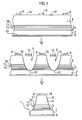
- the first step is on a substrate wafer 2, which consists of GaAs, for example organometallic gas phase epitaxy (MOVPE) a layer sequence 3 applied.
- This sequence of layers exists, for example made of InGaAsP and has an active zone 17.
- the active one Zone 17 is, for example, a pn junction of a light emitting diode.
- the layer sequence 3 has z. B. an n-type 15 and a p-type InGaAlP epitaxial layer 16 on.
- the active zone 17 is designed to emit light emits if it receives an electric current and / or that it generates an electrical voltage, if she receives light. Such active zones and the person skilled in the art is familiar with the associated production processes and are therefore no longer described here.
- a window layer 4 for example consists of GaP or AlGaAs.
- This semiconductor material has a larger band gap than InGaAlP and is therefore for and / or from the active zone received light translucent.
- the next step is to apply a for example made of metal, oxide or organic paint Mesa mask on top 14 of window layer 4 and the second contact metallizations 9 in the composite Substrate wafer 2, layer sequence 3, window layer 4 and the first and second contact metallizations 8, 9 by means of dry etching (indicated by the arrows 10) a plurality of Mesa trenches 5 etched with curved mesa flanks 6.
- the etching parameters become such changed that with increasing etching depth the ratio of vertical etching rate is increased to horizontal etching rate. Thereby the curved mesa flanks are created.
- the depth of this Mesa trenches 5 are chosen so that the window layer 4 and the layer sequence 3 are completely severed and the Substrate wafer 2 is only etched.
- dry etching for example, be used as a suitable known dry reactive ion etching (RIE for R eactive I on E tching), plasma etching, or another the art.
- RIE dry reactive ion etching
- CH 4 / Ar / H 2 / Cl 2 / BCl 3 or CH 4 / Ar / H 2 / Cl 2 / SiCl 4 is used as the etching gas mixture for RIE.
- the concentration of Cl 2 in the etching gas mixture is changed during the etching 10.
- the arrangement of the mesa trenches 5 can be selected in this way, for example be that the semiconductor body 1, as shown in Figure 4, Mesa curvature on all four side surfaces exhibit.
- the mesa trenches are, for example, in a square grid 18 arranged.
- the semiconductor wafer is after the etching of the mesa trenches 5 in these along the dividing lines 11 severed and thus to a plurality of semiconductor bodies 1 with mesa flanks 6 isolated.
- semiconductor bodies 1 manufactured, the at least one from outside the semiconductor body 1 have a concave side surface 6.
- the semiconductor body 1 of Figure 2 differs from that Semiconductor bodies according to FIG. 1 in that it has mesa flanks 6 has a roughening 12.
- This roughening 12 can, for example, by a suitable setting of the Dry etching parameters are generated when etching the mesa trenches 5.
- the depth of the roughening 12 can for example be between 50 and 300 microns are. Other than that, there is no difference between the method of manufacturing a plurality of such Semiconductor body and that described in connection with Figure 1 Method.
Landscapes
- Led Devices (AREA)
- Drying Of Semiconductors (AREA)
- Light Receiving Elements (AREA)
Applications Claiming Priority (3)
| Application Number | Priority Date | Filing Date | Title |
|---|---|---|---|
| DE19632626A DE19632626A1 (de) | 1996-08-13 | 1996-08-13 | Verfahren zum Herstellen von Halbleiterkörpern mit MOVPE-Schichtenfolge |
| DE19632626 | 1996-08-13 | ||
| EP97937453A EP0944918B9 (fr) | 1996-08-13 | 1997-08-13 | Procede pour produire des corps semi-conducteurs presentant une succession de couches deposees par epitaxie en phase gazeuse de melanges organometalliques |
Related Parent Applications (1)
| Application Number | Title | Priority Date | Filing Date |
|---|---|---|---|
| EP97937453A Division EP0944918B9 (fr) | 1996-08-13 | 1997-08-13 | Procede pour produire des corps semi-conducteurs presentant une succession de couches deposees par epitaxie en phase gazeuse de melanges organometalliques |
Publications (2)
| Publication Number | Publication Date |
|---|---|
| EP1347504A2 true EP1347504A2 (fr) | 2003-09-24 |
| EP1347504A3 EP1347504A3 (fr) | 2003-11-26 |
Family
ID=7802533
Family Applications (2)
| Application Number | Title | Priority Date | Filing Date |
|---|---|---|---|
| EP03012549A Withdrawn EP1347504A3 (fr) | 1996-08-13 | 1997-08-13 | Procédé pour produire des corps à semi-conducteurs présentant une succession de couches deposées par MOVPE |
| EP97937453A Expired - Lifetime EP0944918B9 (fr) | 1996-08-13 | 1997-08-13 | Procede pour produire des corps semi-conducteurs presentant une succession de couches deposees par epitaxie en phase gazeuse de melanges organometalliques |
Family Applications After (1)
| Application Number | Title | Priority Date | Filing Date |
|---|---|---|---|
| EP97937453A Expired - Lifetime EP0944918B9 (fr) | 1996-08-13 | 1997-08-13 | Procede pour produire des corps semi-conducteurs presentant une succession de couches deposees par epitaxie en phase gazeuse de melanges organometalliques |
Country Status (7)
| Country | Link |
|---|---|
| US (1) | US6177352B1 (fr) |
| EP (2) | EP1347504A3 (fr) |
| JP (1) | JP3863569B2 (fr) |
| CN (1) | CN1132231C (fr) |
| DE (2) | DE19632626A1 (fr) |
| TW (1) | TW432729B (fr) |
| WO (1) | WO1998007187A1 (fr) |
Cited By (2)
| Publication number | Priority date | Publication date | Assignee | Title |
|---|---|---|---|---|
| US8847241B2 (en) | 2010-04-01 | 2014-09-30 | Jenoptik Polymer Systems Gmbh | Surface-emitting semiconductor light-emitting diode |
| WO2025149575A1 (fr) * | 2024-01-12 | 2025-07-17 | Ams-Osram International Gmbh | Dispositif électroluminescent avec au moins un puits quantique sacrificiel |
Families Citing this family (33)
| Publication number | Priority date | Publication date | Assignee | Title |
|---|---|---|---|---|
| DE19828970C2 (de) * | 1998-06-29 | 2000-05-18 | Siemens Ag | Verfahren zur Herstellung und Vereinzelung von Halbleiter-Lichtemissionsdioden |
| US6277757B1 (en) * | 1999-06-01 | 2001-08-21 | Winbond Electronics Corp. | Methods to modify wet by dry etched via profile |
| TW502458B (en) | 1999-06-09 | 2002-09-11 | Toshiba Corp | Bonding type semiconductor substrate, semiconductor light emission element and manufacturing method thereof |
| US7015516B2 (en) | 2000-11-16 | 2006-03-21 | Gelcore Llc | Led packages having improved light extraction |
| US6887733B2 (en) * | 2002-09-11 | 2005-05-03 | Osram Opto Semiconductors (Malaysia) Sdn. Bhd | Method of fabricating electronic devices |
| US20040048033A1 (en) * | 2002-09-11 | 2004-03-11 | Osram Opto Semiconductors (Malaysia) Sdn. Bhd. | Oled devices with improved encapsulation |
| US7224116B2 (en) * | 2002-09-11 | 2007-05-29 | Osram Opto Semiconductors Gmbh | Encapsulation of active electronic devices |
| US7193364B2 (en) * | 2002-09-12 | 2007-03-20 | Osram Opto Semiconductors (Malaysia) Sdn. Bhd | Encapsulation for organic devices |
| US20040238846A1 (en) * | 2003-05-30 | 2004-12-02 | Georg Wittmann | Organic electronic device |
| US7439551B2 (en) * | 2004-07-08 | 2008-10-21 | Sharp Kabushiki Kaisha | Nitride-based compound semiconductor light emitting device |
| JP4371956B2 (ja) * | 2004-09-02 | 2009-11-25 | シャープ株式会社 | 窒化物系化合物半導体発光素子およびその製造方法 |
| US7352006B2 (en) * | 2004-09-28 | 2008-04-01 | Goldeneye, Inc. | Light emitting diodes exhibiting both high reflectivity and high light extraction |
| US7335576B2 (en) * | 2004-10-08 | 2008-02-26 | Irvine Sensors Corp. | Method for precision integrated circuit die singulation using differential etch rates |
| US20060145599A1 (en) * | 2005-01-04 | 2006-07-06 | Reza Stegamat | OLEDs with phosphors |
| US7563625B2 (en) * | 2005-01-11 | 2009-07-21 | SemiLEDs Optoelectronics Co., Ltd. | Method of making light-emitting diodes (LEDs) with improved light extraction by roughening |
| KR100630736B1 (ko) * | 2005-01-28 | 2006-10-02 | 삼성전자주식회사 | 반도체 소자의 범프 및 제조 방법 |
| JP4767035B2 (ja) * | 2005-04-12 | 2011-09-07 | シャープ株式会社 | 窒化物系半導体発光素子およびその製造方法 |
| EP1763075A1 (fr) | 2005-09-13 | 2007-03-14 | Irvine Sensors Corporation | Méthode de division de circuits intégrés de précision utilisant des vitesses de gravure différentielles. |
| JP2008091862A (ja) * | 2006-09-08 | 2008-04-17 | Sharp Corp | 窒化物半導体発光素子および窒化物半導体発光素子の製造方法 |
| JP2008117824A (ja) * | 2006-11-01 | 2008-05-22 | Sharp Corp | 窒化物系半導体素子の製造方法 |
| TWI344707B (en) * | 2007-04-20 | 2011-07-01 | Huga Optotech Inc | Semiconductor light-emitting device with high light extraction efficiency |
| US7687810B2 (en) * | 2007-10-22 | 2010-03-30 | Philips Lumileds Lighting Company, Llc | Robust LED structure for substrate lift-off |
| KR20120091839A (ko) * | 2011-02-10 | 2012-08-20 | 삼성전자주식회사 | 플립칩 발광소자 패키지 및 그 제조 방법 |
| US8871613B2 (en) * | 2012-06-18 | 2014-10-28 | Semiconductor Components Industries, Llc | Semiconductor die singulation method |
| CN105765740B (zh) * | 2013-10-07 | 2018-10-23 | 廉洪瑞 | 衬底和发光二极管 |
| CN104752306B (zh) * | 2013-12-31 | 2018-03-09 | 北京北方华创微电子装备有限公司 | 在氮化镓层上刻蚀隔离槽的处理方法 |
| US10615222B2 (en) * | 2014-08-21 | 2020-04-07 | The University Of Hong Kong | Flexible GAN light-emitting diodes |
| DE102014114613B4 (de) | 2014-10-08 | 2023-10-12 | OSRAM Opto Semiconductors Gesellschaft mit beschränkter Haftung | Strahlungsemittierender Halbleiterchip, Verfahren zur Herstellung einer Vielzahl an strahlungsemittierenden Halbleiterchips und optoelektronisches Bauelement mit einem strahlungsemittierenden Halbleiterchip |
| CN105742174A (zh) * | 2014-12-11 | 2016-07-06 | 北京北方微电子基地设备工艺研究中心有限责任公司 | 一种AlGaInP基多层结构的深槽刻蚀方法 |
| CN107507770B (zh) * | 2017-06-19 | 2019-11-12 | 青岛海信宽带多媒体技术有限公司 | 一种ⅲ-ⅴ族半导体材料刻蚀方法 |
| JP2019149472A (ja) * | 2018-02-27 | 2019-09-05 | 株式会社東芝 | 半導体装置及びダイシング方法 |
| WO2022047586A1 (fr) * | 2020-09-02 | 2022-03-10 | Vuereal Inc. | Structure de microdispositif à puce retournée |
| CN119545996A (zh) * | 2024-09-25 | 2025-02-28 | 南方科技大学 | 一种侧壁倾斜的红光Micro-LED及其刻蚀方法 |
Family Cites Families (10)
| Publication number | Priority date | Publication date | Assignee | Title |
|---|---|---|---|---|
| US4403241A (en) * | 1980-08-22 | 1983-09-06 | Bell Telephone Laboratories, Incorporated | Method for etching III-V semiconductors and devices made by this method |
| US4393574A (en) * | 1980-12-05 | 1983-07-19 | Kabushiki Kaisha Daini Seikosha | Method for fabricating integrated circuits |
| US4354898A (en) * | 1981-06-24 | 1982-10-19 | Bell Telephone Laboratories, Incorporated | Method of preferentially etching optically flat mirror facets in InGaAsP/InP heterostructures |
| JPS60117631A (ja) * | 1983-11-30 | 1985-06-25 | Toshiba Corp | 化合物半導体のドライエッチング方法 |
| US4984035A (en) * | 1984-11-26 | 1991-01-08 | Hitachi Cable, Ltd. | Monolithic light emitting diode array |
| US4786359A (en) * | 1987-06-24 | 1988-11-22 | Tegal Corporation | Xenon enhanced plasma etch |
| JP3077316B2 (ja) * | 1991-10-30 | 2000-08-14 | 富士電機株式会社 | 集積回路装置 |
| US5309001A (en) * | 1991-11-25 | 1994-05-03 | Sharp Kabushiki Kaisha | Light-emitting diode having a surface electrode of a tree-like form |
| US5233204A (en) * | 1992-01-10 | 1993-08-03 | Hewlett-Packard Company | Light-emitting diode with a thick transparent layer |
| DE4305296C3 (de) * | 1993-02-20 | 1999-07-15 | Vishay Semiconductor Gmbh | Verfahren zum Herstellen einer strahlungsemittierenden Diode |
-
1996
- 1996-08-13 DE DE19632626A patent/DE19632626A1/de not_active Withdrawn
-
1997
- 1997-08-13 DE DE59710312T patent/DE59710312D1/de not_active Expired - Fee Related
- 1997-08-13 EP EP03012549A patent/EP1347504A3/fr not_active Withdrawn
- 1997-08-13 JP JP50930098A patent/JP3863569B2/ja not_active Expired - Fee Related
- 1997-08-13 TW TW086111596A patent/TW432729B/zh not_active IP Right Cessation
- 1997-08-13 EP EP97937453A patent/EP0944918B9/fr not_active Expired - Lifetime
- 1997-08-13 CN CN97197326A patent/CN1132231C/zh not_active Expired - Fee Related
- 1997-08-13 WO PCT/DE1997/001738 patent/WO1998007187A1/fr not_active Ceased
-
1999
- 1999-02-16 US US09/250,868 patent/US6177352B1/en not_active Expired - Fee Related
Non-Patent Citations (1)
| Title |
|---|
| None * |
Cited By (2)
| Publication number | Priority date | Publication date | Assignee | Title |
|---|---|---|---|---|
| US8847241B2 (en) | 2010-04-01 | 2014-09-30 | Jenoptik Polymer Systems Gmbh | Surface-emitting semiconductor light-emitting diode |
| WO2025149575A1 (fr) * | 2024-01-12 | 2025-07-17 | Ams-Osram International Gmbh | Dispositif électroluminescent avec au moins un puits quantique sacrificiel |
Also Published As
| Publication number | Publication date |
|---|---|
| CN1228198A (zh) | 1999-09-08 |
| EP0944918A1 (fr) | 1999-09-29 |
| WO1998007187A1 (fr) | 1998-02-19 |
| EP0944918B1 (fr) | 2003-06-18 |
| TW432729B (en) | 2001-05-01 |
| JP3863569B2 (ja) | 2006-12-27 |
| DE19632626A1 (de) | 1998-02-19 |
| DE59710312D1 (de) | 2003-07-24 |
| EP1347504A3 (fr) | 2003-11-26 |
| JP2000516397A (ja) | 2000-12-05 |
| CN1132231C (zh) | 2003-12-24 |
| US6177352B1 (en) | 2001-01-23 |
| EP0944918B9 (fr) | 2004-01-02 |
Similar Documents
| Publication | Publication Date | Title |
|---|---|---|
| EP0944918B1 (fr) | Procede pour produire des corps semi-conducteurs presentant une succession de couches deposees par epitaxie en phase gazeuse de melanges organometalliques | |
| DE4305296C3 (de) | Verfahren zum Herstellen einer strahlungsemittierenden Diode | |
| DE102012217640B4 (de) | Optoelektronisches Bauelement und Verfahren zu seiner Herstellung | |
| EP2276075A1 (fr) | Disposiif semi-conducteur emetteur de rayonnements et procédé de sa manufacture | |
| EP1920508B1 (fr) | Procédé pour séparer latéralement une plaquette de semi-conducteurs empilés | |
| DE10245628A1 (de) | Elektromagnetische Strahlung emittierender Halbleiterchip und Verfahren zu dessen Herstellung | |
| EP1592072B1 (fr) | Dispositif semiconducteur optoélectronique et son procédé de fabrication | |
| DE102008050538A1 (de) | Optoelektronisches Bauelement und Verfahren zu dessen Herstellung | |
| DE102007004304A1 (de) | Dünnfilm-Leuchtdioden-Chip und Verfahren zur Herstellung eines Dünnfilm-Leuchtdioden-Chips | |
| DE2608562C2 (fr) | ||
| DE112015000850B4 (de) | Verfahren zur Herstellung einer Mehrzahl von Halbleiterbauelementen und Halbleiterbauelement | |
| DE2554029C2 (de) | Verfahren zur Erzeugung optoelektronischer Anordnungen | |
| DE10032246A1 (de) | Lumineszenzdiodenchip auf der Basis von InGaN und Verfahren zu dessen Herstellung | |
| DE102019131422A1 (de) | Optoelektronisches Bauelement und Verfahren zu dessen Herstellung | |
| DE102014111482A1 (de) | Optoelektronischer Halbleiterchip und Verfahren zu dessen Herstellung | |
| DE102014114194B4 (de) | Optoelektronischer Halbleiterchip und Verfahren zu dessen Herstellung | |
| DE102011017097A1 (de) | Verfahren zur Herstellung eines Halbleiterkörpers | |
| WO2015181005A1 (fr) | Puce de semi-conducteur optoélectronique et procédé pour la fabriquer | |
| WO2019215183A1 (fr) | Procédé de sectionnement d'un corps semi-conducteur à croissance épitaxiale et puce semi-conductrice | |
| DE102012112771A1 (de) | Verfahren zur Herstellung eines optoelektronischen Halbleiterchips und optoelektronischer Halbleiterchip | |
| DE102022119108A1 (de) | Optoelektronisches halbleiterbauelement und verfahren zur herstellung zumindest eines optoelektronischen halbleiterbauelements | |
| DE102021109986A1 (de) | Verfahren zur Herstellung eines Licht emittierenden Halbleiterchips und Licht emittierender Halbleiterchip | |
| EP1649497B1 (fr) | Procede de fabrication d'une pluralite de puces a semi-conducteur optoelectroniques et puce a semi-conducteur optoelectronique ainsi obtenue | |
| DE102020200468A1 (de) | Halbleiterlaserdiode und verfahren zur herstellung einer halbleiterlaserdiode | |
| WO2020007710A1 (fr) | Composant émettant un rayonnement et procédé de fabrication d'un composant émettant un rayonnement |
Legal Events
| Date | Code | Title | Description |
|---|---|---|---|
| PUAI | Public reference made under article 153(3) epc to a published international application that has entered the european phase |
Free format text: ORIGINAL CODE: 0009012 |
|
| AC | Divisional application: reference to earlier application |
Ref document number: 0944918 Country of ref document: EP Kind code of ref document: P |
|
| AK | Designated contracting states |
Kind code of ref document: A2 Designated state(s): DE FR GB |
|
| PUAL | Search report despatched |
Free format text: ORIGINAL CODE: 0009013 |
|
| RIN1 | Information on inventor provided before grant (corrected) |
Inventor name: SCHOENFELD, OLAF Inventor name: NIRSCHL, ERNST |
|
| AK | Designated contracting states |
Kind code of ref document: A3 Designated state(s): DE FR GB |
|
| 17P | Request for examination filed |
Effective date: 20040224 |
|
| AKX | Designation fees paid |
Designated state(s): DE |
|
| 17Q | First examination report despatched |
Effective date: 20061017 |
|
| RAP1 | Party data changed (applicant data changed or rights of an application transferred) |
Owner name: OSRAM OPTO SEMICONDUCTORS GMBH |
|
| RAP1 | Party data changed (applicant data changed or rights of an application transferred) |
Owner name: OSRAM OPTO SEMICONDUCTORS GMBH |
|
| STAA | Information on the status of an ep patent application or granted ep patent |
Free format text: STATUS: THE APPLICATION IS DEEMED TO BE WITHDRAWN |
|
| 18D | Application deemed to be withdrawn |
Effective date: 20100302 |