EP1353401A1 - Antenne à directivité variable - Google Patents
Antenne à directivité variable Download PDFInfo
- Publication number
- EP1353401A1 EP1353401A1 EP03396030A EP03396030A EP1353401A1 EP 1353401 A1 EP1353401 A1 EP 1353401A1 EP 03396030 A EP03396030 A EP 03396030A EP 03396030 A EP03396030 A EP 03396030A EP 1353401 A1 EP1353401 A1 EP 1353401A1
- Authority
- EP
- European Patent Office
- Prior art keywords
- antenna
- radio apparatus
- conductive element
- directivity pattern
- conductive
- Prior art date
- Legal status (The legal status is an assumption and is not a legal conclusion. Google has not performed a legal analysis and makes no representation as to the accuracy of the status listed.)
- Granted
Links
- 230000005855 radiation Effects 0.000 claims abstract description 7
- 239000004020 conductor Substances 0.000 claims description 16
- 238000007493 shaping process Methods 0.000 claims description 3
- PEZNEXFPRSOYPL-UHFFFAOYSA-N (bis(trifluoroacetoxy)iodo)benzene Chemical compound FC(F)(F)C(=O)OI(OC(=O)C(F)(F)F)C1=CC=CC=C1 PEZNEXFPRSOYPL-UHFFFAOYSA-N 0.000 claims 1
- 230000004075 alteration Effects 0.000 description 2
- 230000000694 effects Effects 0.000 description 2
- 230000001681 protective effect Effects 0.000 description 2
- 238000007792 addition Methods 0.000 description 1
- 230000002238 attenuated effect Effects 0.000 description 1
- 238000004891 communication Methods 0.000 description 1
- 230000001419 dependent effect Effects 0.000 description 1
- 238000004519 manufacturing process Methods 0.000 description 1
- 239000000463 material Substances 0.000 description 1
- 238000000034 method Methods 0.000 description 1
- 238000010295 mobile communication Methods 0.000 description 1
- 230000003071 parasitic effect Effects 0.000 description 1
Images


Classifications
-
- H—ELECTRICITY
- H01—ELECTRIC ELEMENTS
- H01Q—ANTENNAS, i.e. RADIO AERIALS
- H01Q1/00—Details of, or arrangements associated with, antennas
- H01Q1/12—Supports; Mounting means
- H01Q1/22—Supports; Mounting means by structural association with other equipment or articles
- H01Q1/24—Supports; Mounting means by structural association with other equipment or articles with receiving set
- H01Q1/241—Supports; Mounting means by structural association with other equipment or articles with receiving set used in mobile communications, e.g. GSM
- H01Q1/242—Supports; Mounting means by structural association with other equipment or articles with receiving set used in mobile communications, e.g. GSM specially adapted for hand-held use
- H01Q1/245—Supports; Mounting means by structural association with other equipment or articles with receiving set used in mobile communications, e.g. GSM specially adapted for hand-held use with means for shaping the antenna pattern, e.g. in order to protect user against rf exposure
-
- H—ELECTRICITY
- H01—ELECTRIC ELEMENTS
- H01Q—ANTENNAS, i.e. RADIO AERIALS
- H01Q1/00—Details of, or arrangements associated with, antennas
- H01Q1/12—Supports; Mounting means
- H01Q1/22—Supports; Mounting means by structural association with other equipment or articles
- H01Q1/24—Supports; Mounting means by structural association with other equipment or articles with receiving set
- H01Q1/241—Supports; Mounting means by structural association with other equipment or articles with receiving set used in mobile communications, e.g. GSM
- H01Q1/242—Supports; Mounting means by structural association with other equipment or articles with receiving set used in mobile communications, e.g. GSM specially adapted for hand-held use
-
- H—ELECTRICITY
- H01—ELECTRIC ELEMENTS
- H01Q—ANTENNAS, i.e. RADIO AERIALS
- H01Q1/00—Details of, or arrangements associated with, antennas
- H01Q1/36—Structural form of radiating elements, e.g. cone, spiral, umbrella; Particular materials used therewith
- H01Q1/362—Structural form of radiating elements, e.g. cone, spiral, umbrella; Particular materials used therewith for broadside radiating helical antennas
-
- H—ELECTRICITY
- H01—ELECTRIC ELEMENTS
- H01Q—ANTENNAS, i.e. RADIO AERIALS
- H01Q11/00—Electrically-long antennas having dimensions more than twice the shortest operating wavelength and consisting of conductive active radiating elements
- H01Q11/02—Non-resonant antennas, e.g. travelling-wave antenna
- H01Q11/08—Helical antennas
-
- H—ELECTRICITY
- H01—ELECTRIC ELEMENTS
- H01Q—ANTENNAS, i.e. RADIO AERIALS
- H01Q19/00—Combinations of primary active antenna elements and units with secondary devices, e.g. with quasi-optical devices, for giving the antenna a desired directional characteristic
- H01Q19/005—Patch antenna using one or more coplanar parasitic elements
Definitions
- the invention relates to an antenna which is intended especially for radio telephones and the directivity pattern of which can be altered controllably.
- the invention further relates to a radio telephone having such an antenna.
- the above-mentioned desirable characteristics are achieved with a whip antenna having a large ground plane, for its directivity pattern is circular on the plane perpendicular to the axis of the whip.
- the ground plane is the body of the radio apparatus, which is relatively small and indefinitely shaped from the antenna standpoint. Therefore, the directivity pattern may have considerable alternation.
- the shape of the directivity pattern of a conventional whip antenna of a mobile phone varies uncontrollably so that radiation is directed towards the user's head, too.
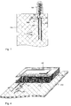
- Figs. 1a,b show an example of such a structure.
- Fig. 1a shows a portion of the body 110 of a mobile phone and, above that, a small antenna circuit board 120 on the front side of which there is a meander-type radiating element 121. This is connected by its bottom end to the antenna port through a feed conductor 125.
- a conductive patch 122 which covers a major part of the radiating element. When the phone is in the use position, the conductive patch 122 stands between the radiating element and the user's head.
- the conductive patch is connected to signal ground GND so that it does not function as a significant parasitic radiator. Instead, it functions as a surface reflecting radio waves, attenuating radiation in the direction of the user's head.
- a drawback of this solution is that also the reception characteristic of the antenna deteriorate in said direction.
- An object of the invention is to reduce the above-described disadvantages associated with the prior art.
- An antenna according to the invention is characterized in that which is specified in the independent claim 1.
- a radio telephone according to the invention is characterized in that which is specified in the independent claim 10.
- Preferred embodiments of the invention are presented in the dependent claims.
- At least one conductive element is added to the antenna structure of a radio telephone in order to change the directivity pattern of the antenna.
- a conductive element is connected to signal ground at a point relatively near the feed point of the antenna.
- the conductive element includes a part the length of which is about a quarter-wave length at the operating frequency of the antenna and which is directed from the ground point to a direction opposite to the feeding direction of the radiating element. This part is used to equalize the directivity pattern of the antenna in the receiving band.
- the conductive element includes a second part which is substantially shorter and directed from the ground point to the feeding direction of the radiating element. The second part is used to set a notch in the directivity pattern at transmitting band frequencies so that it is in a desired direction.
- An advantage of the invention is that the directivity pattern of an antenna can be shaped separately in the transmitting and receiving bands of a given radio system. This means that the directivity pattern can be kept relatively even in the receiving band despite the fact that a directivity pattern notch is provided in the transmitting band.
- Another advantage of the invention is that when using an external antenna, said notch can be achieved through an internal arrangement in the radio telephone without additional elements in the external antenna.
- a further advantage of the invention is that the arrangement according to the invention is simple.
- Fig. 1 was already discussed in conjunction with the description of the prior art.
- Fig. 2 shows enlarged an example of an antenna structure according to the invention.
- the radiating element proper is a helix conductor 220 outside the covers of a radio telephone, placed within a protective sheath.
- the helix may be dimensioned so as to function in frequency bands of two radio systems.
- a feed conductor 225 an extension to the helix conductor, is galvanically connected to a circuit board 210 in the radio telephone at a feed point F of the antenna.
- the feed point F is connected via a duplex filter or antenna switch to the transmitter and receiver of the radio telephone.
- the antenna structure comprises a conductive strip 230 according to the invention on the surface of the circuit board 210.
- the conductive strip 230 is connected to signal ground GND relatively close to the feed point F .
- a thick broken line represents the signal ground. It may be located on the back surface of the circuit board and, in the case of a multilayer board, in intermediate layers as well. "Relatively close” means here that the distance between the ground point G of the conductive strip and the feed point F of the antenna is smaller than a tenth of the wavelength corresponding to the operating frequency.
- the ground point G divides the conductive strip into a first part 231 and a second part 232.
- the length of the first part substantially equals a quarter of the wavelength, and the first part is directed from the ground point to a direction opposite to the feeding direction of the radiating element.
- the second part 232 of the conductive element 230 is substantially shorter than the first part, and it is directed from the ground point G to the feeding direction of the radiating element.
- the first part 231 of the conductive element according to the invention is used to equalize the antenna directivity pattern in the receiving band. This is based on the fact that the antenna structure becomes more regular, dipole-like, removing distinct notches caused in the directivity pattern by the radio telephone body and other conductors functioning as signal ground. Since the shape and location of signal ground e.g. in a circuit board of the radio telephone are indefinable from the antenna standpoint, the exact optimum length of the first part 231 of the conductive element must be found experimentally.
- the second part 232 of the conductive element is used to move a notch of the directivity pattern affecting in the transmitting band to the desired direction.
- Fig. 3 shows a second example of an antenna structure according to the invention.
- the radiating element proper 320 is a helix conductor.
- a feed conductor 325 which is an extension to the helix conductor, is galvanically connected to the radio telephone circuit board 310 at an antenna feed point F , as in Fig. 2.
- the difference is that now the antenna structure comprises not one but two conductive strips according to the invention.
- the first conductive strip 330 is nearly identical with strip 230 in Fig. 2. It has a first ground point G1 , from which there extend in different directions a first part 331, the length of which is substantially a quarter of the wavelength, and a second part 332, which is short compared to the first part.
- the second part has a portion which is transversal with respect to the longitudinal direction of the whole strip, and a portion in the longitudinal direction of the whole strip.
- the second conductive strip 340 according to the invention is connected to signal ground GND at a second ground point G2 , which, like the first ground point G1 , is relatively near the antenna feed point F .
- the second ground point G2 is at the end of the second conductive strip, and the second conductive strip extends therefrom, away from the radiating element and the feed conductor thereof.
- the second conductive element 340 is thus intended only for shaping the directivity pattern in the receiving band. Using two strips, the directivity pattern in the receiving band can be shaped even more round than when using one strip. Moreover, the second conductive strip enhances the independence of the tuning of the directivity patterns in the transmitting and receiving bands.
- Fig. 4 shows a third example of an antenna structure according to the invention.
- the radiating element proper 420 is now a conductive plane elevated from the radio telephone circuit board 410.
- the circuit board 410 has a ground plane 415 below the radiating plane 420, which is a part of the signal ground.
- the radiating plane and ground plane are interconnected at a point through a short-circuit conductor 422, which means the antenna in question is a planar inverted-F antenna (PIFA).
- PIFA planar inverted-F antenna
- a feed conductor 425 of the spring contact type extends out from the edge of the radiating plane and is galvanically connected to an antenna feed point F on the circuit board 410. In this example the latter is quadrangular and surrounded by the ground plane 415 from three sides.
- a first conductive element 431 is connected to the ground plane.
- the first conductive element is a meander-type conductive strip on the surface of the circuit board 410 and it is directed perpendicularly away from the PIFA, as observed from the ground plane connecting point G1 .
- a second conductive element 432 is connected to the ground plane. This is a straight conductive strip on the surface of the circuit board 410, directed perpendicularly away from the PIFA, as observed from the ground plane connecting point.
- the radiating plane 420 is divided by the slot in the plane into two branches so that the PIFA has two operating frequency bands.
- the conductive elements according to the invention can be used to affect the directivity characteristics of the antenna in either one of the bands.
- Fig. 4 also shows a portion of the dielectric support frame 470 for the radiating plane.
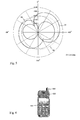
- Fig. 5 shows an example illustrating the directivity characteristics of an antenna structure like the one depicted in Fig. 3, placed in a mobile phone.
- the antenna is dimensioned so as to have two bands for systems GSM900 and GSM1800 (Global System for Mobile telecommunications).
- the transmitting band of the latter for a mobile station is 1710 to 1785 MHz, and receiving band 1805 to 1880 MHz.
- Fig. 5 shows the antenna gain on the horizontal plane when the mobile phone is oriented in an upright position.
- Direction 0° refers to the direction outwards of the front side of the phone, i.e. in the normal use position, towards the user's head.
- Curve 51 shows antenna gain alteration prior to making additions according to the invention in the structure.
- the phone structure in question happens to produce distinct gain notches in directions 30° and 180°. In direction 0°, radiation is relatively strong. This result applies approximately in the whole upper operating band of the antenna, i.e. from 1710 to 1880 MHz.
- the conductive strips according to the invention are dimensioned so as to shape directivity characteristics in the frequency band of the GSM1800 system.
- Curve 52 shows the gain alteration of such an antenna structure at transmitting band frequencies.
- the notch in the gain is now arranged to be in direction 0°, which substantially reduces radiation directed towards the user's head.
- Curve 53 shows gain variation at receiving band frequencies. There are no gain notches at all that would indicate large attenuation, so the antenna receives relatively well from all directions.
- Fig. 6 shows a radio telephone RA with an antenna structure according to the invention.
- the antenna structure comprises an external radiating element 620 placed within a protective sheath, and at least one conductive element 630 within the case of the radio telephone, which conductive element affects the directivity pattern of the antenna.
- the invention does not limit the shapes of antenna elements, nor the shapes of the additional conductive elements, to those described above.
- the conductive elements affecting the directivity pattern may also be conductive wires, for example, and they may be located, say, on the inner surface of the case of the radio apparatus.
- the invention limit the manufacturing method of the antenna or the materials used therein. The inventional idea can be applied in different ways within the scope defined by the independent claim 1.
Landscapes
- Engineering & Computer Science (AREA)
- Computer Networks & Wireless Communication (AREA)
- Support Of Aerials (AREA)
- Details Of Aerials (AREA)
- Variable-Direction Aerials And Aerial Arrays (AREA)
- Aerials With Secondary Devices (AREA)
Applications Claiming Priority (2)
| Application Number | Priority Date | Filing Date | Title |
|---|---|---|---|
| FI20020674A FI121519B (fi) | 2002-04-09 | 2002-04-09 | Suuntakuvioiltaan muokattava antenni |
| FI20020674 | 2002-04-09 |
Publications (2)
| Publication Number | Publication Date |
|---|---|
| EP1353401A1 true EP1353401A1 (fr) | 2003-10-15 |
| EP1353401B1 EP1353401B1 (fr) | 2007-04-25 |
Family
ID=8563724
Family Applications (1)
| Application Number | Title | Priority Date | Filing Date |
|---|---|---|---|
| EP03396030A Expired - Lifetime EP1353401B1 (fr) | 2002-04-09 | 2003-03-31 | Antenne à directivité variable |
Country Status (6)
| Country | Link |
|---|---|
| US (1) | US6967618B2 (fr) |
| EP (1) | EP1353401B1 (fr) |
| CN (1) | CN100346530C (fr) |
| AT (1) | ATE360898T1 (fr) |
| DE (1) | DE60313390T2 (fr) |
| FI (1) | FI121519B (fr) |
Cited By (2)
| Publication number | Priority date | Publication date | Assignee | Title |
|---|---|---|---|---|
| EP1808929A1 (fr) | 2006-01-13 | 2007-07-18 | Research In Motion Limited | Appareil de communication mobile sans fil avec un directeur électroconducteur et méthode correspondante |
| US7423605B2 (en) | 2006-01-13 | 2008-09-09 | Research In Motion Limited | Mobile wireless communications device including an electrically conductive director element and related methods |
Families Citing this family (86)
| Publication number | Priority date | Publication date | Assignee | Title |
|---|---|---|---|---|
| JP2005210521A (ja) * | 2004-01-23 | 2005-08-04 | Sony Corp | アンテナ装置 |
| US7899497B2 (en) | 2004-08-18 | 2011-03-01 | Ruckus Wireless, Inc. | System and method for transmission parameter control for an antenna apparatus with selectable elements |
| US8031129B2 (en) | 2004-08-18 | 2011-10-04 | Ruckus Wireless, Inc. | Dual band dual polarization antenna array |
| US7933628B2 (en) | 2004-08-18 | 2011-04-26 | Ruckus Wireless, Inc. | Transmission and reception parameter control |
| US7696946B2 (en) | 2004-08-18 | 2010-04-13 | Ruckus Wireless, Inc. | Reducing stray capacitance in antenna element switching |
| US7193562B2 (en) | 2004-11-22 | 2007-03-20 | Ruckus Wireless, Inc. | Circuit board having a peripheral antenna apparatus with selectable antenna elements |
| US7965252B2 (en) | 2004-08-18 | 2011-06-21 | Ruckus Wireless, Inc. | Dual polarization antenna array with increased wireless coverage |
| US7362280B2 (en) * | 2004-08-18 | 2008-04-22 | Ruckus Wireless, Inc. | System and method for a minimized antenna apparatus with selectable elements |
| US7880683B2 (en) | 2004-08-18 | 2011-02-01 | Ruckus Wireless, Inc. | Antennas with polarization diversity |
| US7292198B2 (en) | 2004-08-18 | 2007-11-06 | Ruckus Wireless, Inc. | System and method for an omnidirectional planar antenna apparatus with selectable elements |
| US7652632B2 (en) | 2004-08-18 | 2010-01-26 | Ruckus Wireless, Inc. | Multiband omnidirectional planar antenna apparatus with selectable elements |
| US7498996B2 (en) | 2004-08-18 | 2009-03-03 | Ruckus Wireless, Inc. | Antennas with polarization diversity |
| US8619662B2 (en) | 2004-11-05 | 2013-12-31 | Ruckus Wireless, Inc. | Unicast to multicast conversion |
| US8638708B2 (en) | 2004-11-05 | 2014-01-28 | Ruckus Wireless, Inc. | MAC based mapping in IP based communications |
| US7505447B2 (en) | 2004-11-05 | 2009-03-17 | Ruckus Wireless, Inc. | Systems and methods for improved data throughput in communications networks |
| TWI391018B (zh) | 2004-11-05 | 2013-03-21 | Ruckus Wireless Inc | 藉由確認抑制之增強資訊量 |
| CN1934750B (zh) | 2004-11-22 | 2012-07-18 | 鲁库斯无线公司 | 包括具有可选择天线元件的外围天线装置的电路板 |
| US7358912B1 (en) | 2005-06-24 | 2008-04-15 | Ruckus Wireless, Inc. | Coverage antenna apparatus with selectable horizontal and vertical polarization elements |
| US8792414B2 (en) | 2005-07-26 | 2014-07-29 | Ruckus Wireless, Inc. | Coverage enhancement using dynamic antennas |
| US7646343B2 (en) | 2005-06-24 | 2010-01-12 | Ruckus Wireless, Inc. | Multiple-input multiple-output wireless antennas |
| US7893882B2 (en) | 2007-01-08 | 2011-02-22 | Ruckus Wireless, Inc. | Pattern shaping of RF emission patterns |
| CN100385806C (zh) * | 2005-01-28 | 2008-04-30 | 联发科技股份有限公司 | 移动通信装置 |
| FI20055420A0 (fi) | 2005-07-25 | 2005-07-25 | Lk Products Oy | Säädettävä monikaista antenni |
| US7183979B1 (en) * | 2005-08-24 | 2007-02-27 | Accton Technology Corporation | Dual-band patch antenna with slot structure |
| FI119009B (fi) | 2005-10-03 | 2008-06-13 | Pulse Finland Oy | Monikaistainen antennijärjestelmä |
| FI118782B (fi) | 2005-10-14 | 2008-03-14 | Pulse Finland Oy | Säädettävä antenni |
| EP2763443B1 (fr) | 2005-12-01 | 2019-05-22 | Ruckus Wireless, Inc. | Services à la demande par virtualisation de station de base sans fil |
| US7479928B2 (en) | 2006-03-28 | 2009-01-20 | Motorola, Inc. | Antenna radiator assembly and radio communications assembly |
| US7265724B1 (en) * | 2006-03-28 | 2007-09-04 | Motorola Inc. | Communications assembly and antenna assembly with a switched tuning line |
| CN103441984B (zh) | 2006-04-24 | 2017-09-05 | 鲁库斯无线公司 | 安全无线网络中的动态认证 |
| US9071583B2 (en) | 2006-04-24 | 2015-06-30 | Ruckus Wireless, Inc. | Provisioned configuration for automatic wireless connection |
| US9769655B2 (en) | 2006-04-24 | 2017-09-19 | Ruckus Wireless, Inc. | Sharing security keys with headless devices |
| US7639106B2 (en) | 2006-04-28 | 2009-12-29 | Ruckus Wireless, Inc. | PIN diode network for multiband RF coupling |
| TW200803038A (en) * | 2006-06-23 | 2008-01-01 | Wistron Neweb Corp | A flat mini type digital television antenna |
| US8618990B2 (en) | 2011-04-13 | 2013-12-31 | Pulse Finland Oy | Wideband antenna and methods |
| US8670725B2 (en) | 2006-08-18 | 2014-03-11 | Ruckus Wireless, Inc. | Closed-loop automatic channel selection |
| FI20075269A0 (fi) | 2007-04-19 | 2007-04-19 | Pulse Finland Oy | Menetelmä ja järjestely antennin sovittamiseksi |
| US8547899B2 (en) | 2007-07-28 | 2013-10-01 | Ruckus Wireless, Inc. | Wireless network throughput enhancement through channel aware scheduling |
| FI120427B (fi) | 2007-08-30 | 2009-10-15 | Pulse Finland Oy | Säädettävä monikaista-antenni |
| US8355343B2 (en) | 2008-01-11 | 2013-01-15 | Ruckus Wireless, Inc. | Determining associations in a mesh network |
| KR100951228B1 (ko) * | 2008-05-13 | 2010-04-05 | 삼성전기주식회사 | 안테나 |
| US20100214184A1 (en) * | 2009-02-24 | 2010-08-26 | Qualcomm Incorporated | Antenna devices and systems for multi-band coverage in a compact volume |
| US8217843B2 (en) | 2009-03-13 | 2012-07-10 | Ruckus Wireless, Inc. | Adjustment of radiation patterns utilizing a position sensor |
| US8698675B2 (en) | 2009-05-12 | 2014-04-15 | Ruckus Wireless, Inc. | Mountable antenna elements for dual band antenna |
| FI20096134A0 (fi) | 2009-11-03 | 2009-11-03 | Pulse Finland Oy | Säädettävä antenni |
| US9979626B2 (en) | 2009-11-16 | 2018-05-22 | Ruckus Wireless, Inc. | Establishing a mesh network with wired and wireless links |
| US9999087B2 (en) | 2009-11-16 | 2018-06-12 | Ruckus Wireless, Inc. | Determining role assignment in a hybrid mesh network |
| FI20096251A0 (sv) | 2009-11-27 | 2009-11-27 | Pulse Finland Oy | MIMO-antenn |
| JP5637681B2 (ja) * | 2009-12-16 | 2014-12-10 | キヤノン株式会社 | 制御装置、中継装置、それらの制御方法およびプログラム |
| US8847833B2 (en) | 2009-12-29 | 2014-09-30 | Pulse Finland Oy | Loop resonator apparatus and methods for enhanced field control |
| FI20105158A7 (fi) | 2010-02-18 | 2011-08-19 | Pulse Finland Oy | Kuorisäteilijällä varustettu antenni |
| US9406998B2 (en) | 2010-04-21 | 2016-08-02 | Pulse Finland Oy | Distributed multiband antenna and methods |
| US9407012B2 (en) | 2010-09-21 | 2016-08-02 | Ruckus Wireless, Inc. | Antenna with dual polarization and mountable antenna elements |
| FI20115072A0 (fi) | 2011-01-25 | 2011-01-25 | Pulse Finland Oy | Moniresonanssiantenni, -antennimoduuli ja radiolaite |
| US9673507B2 (en) | 2011-02-11 | 2017-06-06 | Pulse Finland Oy | Chassis-excited antenna apparatus and methods |
| US8648752B2 (en) | 2011-02-11 | 2014-02-11 | Pulse Finland Oy | Chassis-excited antenna apparatus and methods |
| CN103858106B (zh) | 2011-05-01 | 2017-04-26 | 鲁库斯无线公司 | 远程电缆接入点复位 |
| CN102354807B (zh) * | 2011-06-24 | 2016-03-09 | 电子科技大学 | 宽带无线数据卡天线 |
| US8866689B2 (en) | 2011-07-07 | 2014-10-21 | Pulse Finland Oy | Multi-band antenna and methods for long term evolution wireless system |
| US9450291B2 (en) | 2011-07-25 | 2016-09-20 | Pulse Finland Oy | Multiband slot loop antenna apparatus and methods |
| US9123990B2 (en) | 2011-10-07 | 2015-09-01 | Pulse Finland Oy | Multi-feed antenna apparatus and methods |
| US9531058B2 (en) | 2011-12-20 | 2016-12-27 | Pulse Finland Oy | Loosely-coupled radio antenna apparatus and methods |
| US9484619B2 (en) | 2011-12-21 | 2016-11-01 | Pulse Finland Oy | Switchable diversity antenna apparatus and methods |
| US8756668B2 (en) | 2012-02-09 | 2014-06-17 | Ruckus Wireless, Inc. | Dynamic PSK for hotspots |
| US9634403B2 (en) | 2012-02-14 | 2017-04-25 | Ruckus Wireless, Inc. | Radio frequency emission pattern shaping |
| US10186750B2 (en) | 2012-02-14 | 2019-01-22 | Arris Enterprises Llc | Radio frequency antenna array with spacing element |
| US9092610B2 (en) | 2012-04-04 | 2015-07-28 | Ruckus Wireless, Inc. | Key assignment for a brand |
| US8988296B2 (en) | 2012-04-04 | 2015-03-24 | Pulse Finland Oy | Compact polarized antenna and methods |
| US9570799B2 (en) | 2012-09-07 | 2017-02-14 | Ruckus Wireless, Inc. | Multiband monopole antenna apparatus with ground plane aperture |
| US9979078B2 (en) | 2012-10-25 | 2018-05-22 | Pulse Finland Oy | Modular cell antenna apparatus and methods |
| US10069209B2 (en) | 2012-11-06 | 2018-09-04 | Pulse Finland Oy | Capacitively coupled antenna apparatus and methods |
| US9647338B2 (en) | 2013-03-11 | 2017-05-09 | Pulse Finland Oy | Coupled antenna structure and methods |
| US10079428B2 (en) | 2013-03-11 | 2018-09-18 | Pulse Finland Oy | Coupled antenna structure and methods |
| HK1220050A1 (zh) | 2013-03-15 | 2017-04-21 | Ruckus Wireless, Inc. | 为双频定向天线而设的低频带反射器 |
| US9634383B2 (en) | 2013-06-26 | 2017-04-25 | Pulse Finland Oy | Galvanically separated non-interacting antenna sector apparatus and methods |
| JP6167745B2 (ja) * | 2013-08-13 | 2017-07-26 | 富士通株式会社 | アンテナ装置 |
| US9680212B2 (en) | 2013-11-20 | 2017-06-13 | Pulse Finland Oy | Capacitive grounding methods and apparatus for mobile devices |
| US9590308B2 (en) | 2013-12-03 | 2017-03-07 | Pulse Electronics, Inc. | Reduced surface area antenna apparatus and mobile communications devices incorporating the same |
| US9350081B2 (en) | 2014-01-14 | 2016-05-24 | Pulse Finland Oy | Switchable multi-radiator high band antenna apparatus |
| US9948002B2 (en) | 2014-08-26 | 2018-04-17 | Pulse Finland Oy | Antenna apparatus with an integrated proximity sensor and methods |
| US9973228B2 (en) | 2014-08-26 | 2018-05-15 | Pulse Finland Oy | Antenna apparatus with an integrated proximity sensor and methods |
| US9722308B2 (en) | 2014-08-28 | 2017-08-01 | Pulse Finland Oy | Low passive intermodulation distributed antenna system for multiple-input multiple-output systems and methods of use |
| US9906260B2 (en) | 2015-07-30 | 2018-02-27 | Pulse Finland Oy | Sensor-based closed loop antenna swapping apparatus and methods |
| WO2018072067A1 (fr) * | 2016-10-18 | 2018-04-26 | 深圳市大疆创新科技有限公司 | Composant d'antenne et véhicule aérien sans pilote |
| EP4037099A4 (fr) * | 2019-09-27 | 2022-10-26 | Panasonic Intellectual Property Management Co., Ltd. | Dispositif d'antenne |
| CN112310643B (zh) * | 2020-09-03 | 2021-10-29 | 瑞声新能源发展(常州)有限公司科教城分公司 | 天线模组及应用该天线模组的终端设备 |
Citations (5)
| Publication number | Priority date | Publication date | Assignee | Title |
|---|---|---|---|---|
| EP0367609A2 (fr) * | 1988-11-02 | 1990-05-09 | Motorola, Inc. | Antenne pliante pour des radiotéléphones portatives dans un système cellulaire |
| WO1997044911A1 (fr) * | 1996-05-17 | 1997-11-27 | Ryhaenen Heikki | Procede et dispositif visant a eliminer ou a restreindre localement un champ de rayonnement a frequence radioelectrique |
| JP2000040910A (ja) * | 1998-07-23 | 2000-02-08 | Nippon Antenna Co Ltd | アンテナ給電部および携帯無線機 |
| US20020019247A1 (en) * | 2000-08-07 | 2002-02-14 | Igor Egorov | Antenna |
| EP1271688A1 (fr) * | 2001-06-13 | 2003-01-02 | Kabushiki Kaisha Toshiba | Module radio et appareil de communication radio avec le module radio |
Family Cites Families (15)
| Publication number | Priority date | Publication date | Assignee | Title |
|---|---|---|---|---|
| US6034638A (en) * | 1993-05-27 | 2000-03-07 | Griffith University | Antennas for use in portable communications devices |
| SE512062C2 (sv) | 1993-07-14 | 2000-01-17 | Ericsson Ge Mobile Communicat | Förfarande och anordning för att förbättra effektivitet och bandbredd för en antenn på en bärbar utrustning |
| JPH08307126A (ja) * | 1995-05-09 | 1996-11-22 | Kyocera Corp | アンテナの収納構造 |
| KR960043337A (ko) * | 1995-05-24 | 1996-12-23 | 김광호 | 반사판이 부착된 휴대용 무선기기 안테나 |
| SE509638C2 (sv) * | 1996-06-15 | 1999-02-15 | Allgon Ab | Meanderantennanordning |
| FI110394B (fi) * | 1996-08-06 | 2003-01-15 | Filtronic Lk Oy | Yhdistelmäantenni |
| JP2000165126A (ja) * | 1998-11-30 | 2000-06-16 | Matsushita Electric Ind Co Ltd | アンテナ装置 |
| US6249255B1 (en) * | 1999-04-30 | 2001-06-19 | Nokia Mobile Phones, Limited | Antenna assembly, and associated method, having parasitic element for altering antenna pattern characteristics |
| JP2001257522A (ja) * | 2000-03-09 | 2001-09-21 | Sony Corp | アンテナ装置及び携帯無線機 |
| JP4217938B2 (ja) | 2000-04-20 | 2009-02-04 | ソニー株式会社 | アンテナ装置及び携帯無線機 |
| FI112724B (fi) * | 2000-05-12 | 2003-12-31 | Nokia Corp | Symmetrinen antennirakenne ja menetelmä sen valmistamiseksi sekä antennirakennetta soveltava laajennuskortti |
| JP2002094311A (ja) | 2000-07-14 | 2002-03-29 | Sony Corp | アンテナ装置及び携帯型無線端末 |
| US6229488B1 (en) * | 2000-09-08 | 2001-05-08 | Emtac Technology Corp. | Antenna for receiving signals from GPS and GSM |
| US6606071B2 (en) * | 2001-12-18 | 2003-08-12 | Wistron Neweb Corporation | Multifrequency antenna with a slot-type conductor and a strip-shaped conductor |
| FI119861B (fi) * | 2002-02-01 | 2009-04-15 | Pulse Finland Oy | Tasoantenni |
-
2002
- 2002-04-09 FI FI20020674A patent/FI121519B/fi not_active IP Right Cessation
-
2003
- 2003-03-31 DE DE60313390T patent/DE60313390T2/de not_active Expired - Lifetime
- 2003-03-31 AT AT03396030T patent/ATE360898T1/de not_active IP Right Cessation
- 2003-03-31 EP EP03396030A patent/EP1353401B1/fr not_active Expired - Lifetime
- 2003-04-04 US US10/408,048 patent/US6967618B2/en not_active Expired - Fee Related
- 2003-04-09 CN CNB031103413A patent/CN100346530C/zh not_active Expired - Fee Related
Patent Citations (5)
| Publication number | Priority date | Publication date | Assignee | Title |
|---|---|---|---|---|
| EP0367609A2 (fr) * | 1988-11-02 | 1990-05-09 | Motorola, Inc. | Antenne pliante pour des radiotéléphones portatives dans un système cellulaire |
| WO1997044911A1 (fr) * | 1996-05-17 | 1997-11-27 | Ryhaenen Heikki | Procede et dispositif visant a eliminer ou a restreindre localement un champ de rayonnement a frequence radioelectrique |
| JP2000040910A (ja) * | 1998-07-23 | 2000-02-08 | Nippon Antenna Co Ltd | アンテナ給電部および携帯無線機 |
| US20020019247A1 (en) * | 2000-08-07 | 2002-02-14 | Igor Egorov | Antenna |
| EP1271688A1 (fr) * | 2001-06-13 | 2003-01-02 | Kabushiki Kaisha Toshiba | Module radio et appareil de communication radio avec le module radio |
Non-Patent Citations (2)
| Title |
|---|
| PATENT ABSTRACTS OF JAPAN vol. 2000, no. 05 14 September 2000 (2000-09-14) * |
| VAUGHAN R: "SWITCHED PARASITIC ELEMENTS FOR ANTENNA DIVERSITY", IEEE TRANSACTIONS ON ANTENNAS AND PROPAGATION, IEEE INC. NEW YORK, US, vol. 47, no. 2, February 1999 (1999-02-01), pages 399 - 405, XP000827246, ISSN: 0018-926X * |
Cited By (4)
| Publication number | Priority date | Publication date | Assignee | Title |
|---|---|---|---|---|
| EP1808929A1 (fr) | 2006-01-13 | 2007-07-18 | Research In Motion Limited | Appareil de communication mobile sans fil avec un directeur électroconducteur et méthode correspondante |
| US7423605B2 (en) | 2006-01-13 | 2008-09-09 | Research In Motion Limited | Mobile wireless communications device including an electrically conductive director element and related methods |
| US7830325B2 (en) | 2006-01-13 | 2010-11-09 | Research In Motion Limited | Mobile wireless communications device including an electrically conductive director element and related methods |
| US9214737B2 (en) | 2006-01-13 | 2015-12-15 | Blackberry Limited | Mobile wireless communications device including an electrically conductive director element and related methods |
Also Published As
| Publication number | Publication date |
|---|---|
| FI121519B (fi) | 2010-12-15 |
| DE60313390T2 (de) | 2008-01-03 |
| US6967618B2 (en) | 2005-11-22 |
| FI20020674A0 (fi) | 2002-04-09 |
| CN1450686A (zh) | 2003-10-22 |
| ATE360898T1 (de) | 2007-05-15 |
| US20030189523A1 (en) | 2003-10-09 |
| CN100346530C (zh) | 2007-10-31 |
| FI20020674A7 (fi) | 2003-10-10 |
| DE60313390D1 (de) | 2007-06-06 |
| EP1353401B1 (fr) | 2007-04-25 |
Similar Documents
| Publication | Publication Date | Title |
|---|---|---|
| US6967618B2 (en) | Antenna with variable directional pattern | |
| US8786499B2 (en) | Multiband antenna system and methods | |
| EP1113524B1 (fr) | Structure d'antenne, méthode pour coupler un signal sur la structure d antenne, unité d'antenne et station mobile avec une telle structure d'antenne | |
| CN100361346C (zh) | 移动体通信用宽频带天线 | |
| JP4562845B2 (ja) | 非対称ダイポール・アンテナ組立体 | |
| US7889143B2 (en) | Multiband antenna system and methods | |
| JP2870940B2 (ja) | 車載アンテナ | |
| US6930641B2 (en) | Antenna and radio device using the same | |
| US20130127674A1 (en) | Antenna with cover radiator and methods | |
| EP1629569B1 (fr) | Antenne interne avec fentes | |
| US20230071050A1 (en) | Broadband decoupling radiating elements and base station antennas having such radiating elements | |
| WO2007000483A1 (fr) | Antenne multibande interne | |
| WO1999013528A1 (fr) | Ensemble d'antenne a cadre pour dispositifs de telecommunications | |
| KR20010075231A (ko) | 용량성으로 튜닝된 광대역 안테나 구조 | |
| EP3079203A1 (fr) | Antenne multibande imprimée àlimentée par couplage et système électronique | |
| JP2007151115A (ja) | モノポールアンテナ、及びそれを含むmimoアンテナ | |
| KR20070101168A (ko) | 안테나 장치 및 이를 이용한 멀티 밴드 타입 무선 통신기기 | |
| EP4053996A1 (fr) | Antenne multibande et procédé d'accord d'antenne multibande | |
| CN116195137B (zh) | 天线设备及天线设备阵列 | |
| EP2323217B1 (fr) | Antenne pour communication mimo multimodale dans des dispositifs portables | |
| US6836246B1 (en) | Design of single and multi-band PIFA | |
| KR101049724B1 (ko) | 독립 조절이 가능하고 절곡부를 가지는 다중 대역 안테나 | |
| CN114374082A (zh) | 辐射元件和基站天线 | |
| KR100640339B1 (ko) | 광대역 모노폴 안테나 | |
| KR100538185B1 (ko) | 다중 밴드 내장형 안테나 및 이를 구비하는 무선 통신 장치 |
Legal Events
| Date | Code | Title | Description |
|---|---|---|---|
| PUAI | Public reference made under article 153(3) epc to a published international application that has entered the european phase |
Free format text: ORIGINAL CODE: 0009012 |
|
| AK | Designated contracting states |
Kind code of ref document: A1 Designated state(s): AT BE BG CH CY CZ DE DK EE ES FI FR GB GR HU IE IT LI LU MC NL PT RO SE SI SK TR |
|
| AX | Request for extension of the european patent |
Extension state: AL LT LV MK |
|
| 17P | Request for examination filed |
Effective date: 20031025 |
|
| AKX | Designation fees paid |
Designated state(s): AT BE BG CH CY CZ DE DK EE ES FI FR GB GR HU IE IT LI LU MC NL PT RO SE SI SK TR |
|
| 17Q | First examination report despatched |
Effective date: 20040615 |
|
| RAP1 | Party data changed (applicant data changed or rights of an application transferred) |
Owner name: LK PRODUCTS OY |
|
| GRAP | Despatch of communication of intention to grant a patent |
Free format text: ORIGINAL CODE: EPIDOSNIGR1 |
|
| RAP1 | Party data changed (applicant data changed or rights of an application transferred) |
Owner name: PULSE FINLAND OY |
|
| GRAS | Grant fee paid |
Free format text: ORIGINAL CODE: EPIDOSNIGR3 |
|
| GRAA | (expected) grant |
Free format text: ORIGINAL CODE: 0009210 |
|
| AK | Designated contracting states |
Kind code of ref document: B1 Designated state(s): AT BE BG CH CY CZ DE DK EE ES FI FR GB GR HU IE IT LI LU MC NL PT RO SE SI SK TR |
|
| PG25 | Lapsed in a contracting state [announced via postgrant information from national office to epo] |
Ref country code: FI Free format text: LAPSE BECAUSE OF FAILURE TO SUBMIT A TRANSLATION OF THE DESCRIPTION OR TO PAY THE FEE WITHIN THE PRESCRIBED TIME-LIMIT Effective date: 20070425 Ref country code: CH Free format text: LAPSE BECAUSE OF FAILURE TO SUBMIT A TRANSLATION OF THE DESCRIPTION OR TO PAY THE FEE WITHIN THE PRESCRIBED TIME-LIMIT Effective date: 20070425 Ref country code: LI Free format text: LAPSE BECAUSE OF FAILURE TO SUBMIT A TRANSLATION OF THE DESCRIPTION OR TO PAY THE FEE WITHIN THE PRESCRIBED TIME-LIMIT Effective date: 20070425 |
|
| REG | Reference to a national code |
Ref country code: GB Ref legal event code: FG4D |
|
| REG | Reference to a national code |
Ref country code: IE Ref legal event code: FG4D |
|
| REG | Reference to a national code |
Ref country code: CH Ref legal event code: EP |
|
| REF | Corresponds to: |
Ref document number: 60313390 Country of ref document: DE Date of ref document: 20070606 Kind code of ref document: P |
|
| REG | Reference to a national code |
Ref country code: SE Ref legal event code: TRGR |
|
| PG25 | Lapsed in a contracting state [announced via postgrant information from national office to epo] |
Ref country code: ES Free format text: LAPSE BECAUSE OF FAILURE TO SUBMIT A TRANSLATION OF THE DESCRIPTION OR TO PAY THE FEE WITHIN THE PRESCRIBED TIME-LIMIT Effective date: 20070805 |
|
| PG25 | Lapsed in a contracting state [announced via postgrant information from national office to epo] |
Ref country code: PT Free format text: LAPSE BECAUSE OF FAILURE TO SUBMIT A TRANSLATION OF THE DESCRIPTION OR TO PAY THE FEE WITHIN THE PRESCRIBED TIME-LIMIT Effective date: 20070925 |
|
| ET | Fr: translation filed | ||
| REG | Reference to a national code |
Ref country code: CH Ref legal event code: PL |
|
| NLV1 | Nl: lapsed or annulled due to failure to fulfill the requirements of art. 29p and 29m of the patents act | ||
| PG25 | Lapsed in a contracting state [announced via postgrant information from national office to epo] |
Ref country code: AT Free format text: LAPSE BECAUSE OF FAILURE TO SUBMIT A TRANSLATION OF THE DESCRIPTION OR TO PAY THE FEE WITHIN THE PRESCRIBED TIME-LIMIT Effective date: 20070425 |
|
| PG25 | Lapsed in a contracting state [announced via postgrant information from national office to epo] |
Ref country code: BE Free format text: LAPSE BECAUSE OF FAILURE TO SUBMIT A TRANSLATION OF THE DESCRIPTION OR TO PAY THE FEE WITHIN THE PRESCRIBED TIME-LIMIT Effective date: 20070425 |
|
| PG25 | Lapsed in a contracting state [announced via postgrant information from national office to epo] |
Ref country code: DK Free format text: LAPSE BECAUSE OF FAILURE TO SUBMIT A TRANSLATION OF THE DESCRIPTION OR TO PAY THE FEE WITHIN THE PRESCRIBED TIME-LIMIT Effective date: 20070425 Ref country code: NL Free format text: LAPSE BECAUSE OF FAILURE TO SUBMIT A TRANSLATION OF THE DESCRIPTION OR TO PAY THE FEE WITHIN THE PRESCRIBED TIME-LIMIT Effective date: 20070425 Ref country code: CZ Free format text: LAPSE BECAUSE OF FAILURE TO SUBMIT A TRANSLATION OF THE DESCRIPTION OR TO PAY THE FEE WITHIN THE PRESCRIBED TIME-LIMIT Effective date: 20070425 Ref country code: BG Free format text: LAPSE BECAUSE OF FAILURE TO SUBMIT A TRANSLATION OF THE DESCRIPTION OR TO PAY THE FEE WITHIN THE PRESCRIBED TIME-LIMIT Effective date: 20070725 Ref country code: SI Free format text: LAPSE BECAUSE OF FAILURE TO SUBMIT A TRANSLATION OF THE DESCRIPTION OR TO PAY THE FEE WITHIN THE PRESCRIBED TIME-LIMIT Effective date: 20070425 |
|
| PG25 | Lapsed in a contracting state [announced via postgrant information from national office to epo] |
Ref country code: SK Free format text: LAPSE BECAUSE OF FAILURE TO SUBMIT A TRANSLATION OF THE DESCRIPTION OR TO PAY THE FEE WITHIN THE PRESCRIBED TIME-LIMIT Effective date: 20070425 |
|
| PLBE | No opposition filed within time limit |
Free format text: ORIGINAL CODE: 0009261 |
|
| STAA | Information on the status of an ep patent application or granted ep patent |
Free format text: STATUS: NO OPPOSITION FILED WITHIN TIME LIMIT |
|
| 26N | No opposition filed |
Effective date: 20080128 |
|
| PG25 | Lapsed in a contracting state [announced via postgrant information from national office to epo] |
Ref country code: IT Free format text: LAPSE BECAUSE OF FAILURE TO SUBMIT A TRANSLATION OF THE DESCRIPTION OR TO PAY THE FEE WITHIN THE PRESCRIBED TIME-LIMIT Effective date: 20070425 Ref country code: GR Free format text: LAPSE BECAUSE OF FAILURE TO SUBMIT A TRANSLATION OF THE DESCRIPTION OR TO PAY THE FEE WITHIN THE PRESCRIBED TIME-LIMIT Effective date: 20070726 |
|
| PG25 | Lapsed in a contracting state [announced via postgrant information from national office to epo] |
Ref country code: RO Free format text: LAPSE BECAUSE OF FAILURE TO SUBMIT A TRANSLATION OF THE DESCRIPTION OR TO PAY THE FEE WITHIN THE PRESCRIBED TIME-LIMIT Effective date: 20070425 |
|
| PG25 | Lapsed in a contracting state [announced via postgrant information from national office to epo] |
Ref country code: MC Free format text: LAPSE BECAUSE OF NON-PAYMENT OF DUE FEES Effective date: 20080331 |
|
| PG25 | Lapsed in a contracting state [announced via postgrant information from national office to epo] |
Ref country code: EE Free format text: LAPSE BECAUSE OF FAILURE TO SUBMIT A TRANSLATION OF THE DESCRIPTION OR TO PAY THE FEE WITHIN THE PRESCRIBED TIME-LIMIT Effective date: 20070425 Ref country code: IE Free format text: LAPSE BECAUSE OF NON-PAYMENT OF DUE FEES Effective date: 20080331 |
|
| PG25 | Lapsed in a contracting state [announced via postgrant information from national office to epo] |
Ref country code: CY Free format text: LAPSE BECAUSE OF FAILURE TO SUBMIT A TRANSLATION OF THE DESCRIPTION OR TO PAY THE FEE WITHIN THE PRESCRIBED TIME-LIMIT Effective date: 20070425 |
|
| PGFP | Annual fee paid to national office [announced via postgrant information from national office to epo] |
Ref country code: SE Payment date: 20091218 Year of fee payment: 8 |
|
| PGFP | Annual fee paid to national office [announced via postgrant information from national office to epo] |
Ref country code: FR Payment date: 20100324 Year of fee payment: 8 |
|
| PGFP | Annual fee paid to national office [announced via postgrant information from national office to epo] |
Ref country code: GB Payment date: 20100322 Year of fee payment: 8 |
|
| PG25 | Lapsed in a contracting state [announced via postgrant information from national office to epo] |
Ref country code: LU Free format text: LAPSE BECAUSE OF NON-PAYMENT OF DUE FEES Effective date: 20080331 Ref country code: HU Free format text: LAPSE BECAUSE OF FAILURE TO SUBMIT A TRANSLATION OF THE DESCRIPTION OR TO PAY THE FEE WITHIN THE PRESCRIBED TIME-LIMIT Effective date: 20071026 |
|
| PG25 | Lapsed in a contracting state [announced via postgrant information from national office to epo] |
Ref country code: TR Free format text: LAPSE BECAUSE OF FAILURE TO SUBMIT A TRANSLATION OF THE DESCRIPTION OR TO PAY THE FEE WITHIN THE PRESCRIBED TIME-LIMIT Effective date: 20070425 |
|
| PGFP | Annual fee paid to national office [announced via postgrant information from national office to epo] |
Ref country code: DE Payment date: 20100430 Year of fee payment: 8 |
|
| GBPC | Gb: european patent ceased through non-payment of renewal fee |
Effective date: 20110331 |
|
| REG | Reference to a national code |
Ref country code: SE Ref legal event code: EUG |
|
| REG | Reference to a national code |
Ref country code: FR Ref legal event code: ST Effective date: 20111130 |
|
| PG25 | Lapsed in a contracting state [announced via postgrant information from national office to epo] |
Ref country code: DE Free format text: LAPSE BECAUSE OF NON-PAYMENT OF DUE FEES Effective date: 20111001 Ref country code: FR Free format text: LAPSE BECAUSE OF NON-PAYMENT OF DUE FEES Effective date: 20110331 |
|
| REG | Reference to a national code |
Ref country code: DE Ref legal event code: R119 Ref document number: 60313390 Country of ref document: DE Effective date: 20111001 |
|
| PG25 | Lapsed in a contracting state [announced via postgrant information from national office to epo] |
Ref country code: GB Free format text: LAPSE BECAUSE OF NON-PAYMENT OF DUE FEES Effective date: 20110331 |
|
| PG25 | Lapsed in a contracting state [announced via postgrant information from national office to epo] |
Ref country code: SE Free format text: LAPSE BECAUSE OF NON-PAYMENT OF DUE FEES Effective date: 20110401 |