EP1353446A2 - Système et méthode pour générer des codes cycliques pour le contrôle d'erreurs pour des communications digitales - Google Patents
Système et méthode pour générer des codes cycliques pour le contrôle d'erreurs pour des communications digitales Download PDFInfo
- Publication number
- EP1353446A2 EP1353446A2 EP03007893A EP03007893A EP1353446A2 EP 1353446 A2 EP1353446 A2 EP 1353446A2 EP 03007893 A EP03007893 A EP 03007893A EP 03007893 A EP03007893 A EP 03007893A EP 1353446 A2 EP1353446 A2 EP 1353446A2
- Authority
- EP
- European Patent Office
- Prior art keywords
- information signal
- circuit
- polynomial
- code
- represented
- Prior art date
- Legal status (The legal status is an assumption and is not a legal conclusion. Google has not performed a legal analysis and makes no representation as to the accuracy of the status listed.)
- Granted
Links
Images





Classifications
-
- H—ELECTRICITY
- H03—ELECTRONIC CIRCUITRY
- H03M—CODING; DECODING; CODE CONVERSION IN GENERAL
- H03M13/00—Coding, decoding or code conversion, for error detection or error correction; Coding theory basic assumptions; Coding bounds; Error probability evaluation methods; Channel models; Simulation or testing of codes
- H03M13/03—Error detection or forward error correction by redundancy in data representation, i.e. code words containing more digits than the source words
- H03M13/05—Error detection or forward error correction by redundancy in data representation, i.e. code words containing more digits than the source words using block codes, i.e. a predetermined number of check bits joined to a predetermined number of information bits
- H03M13/09—Error detection only, e.g. using cyclic redundancy check [CRC] codes or single parity bit
- H03M13/091—Parallel or block-wise CRC computation
-
- H—ELECTRICITY
- H03—ELECTRONIC CIRCUITRY
- H03M—CODING; DECODING; CODE CONVERSION IN GENERAL
- H03M13/00—Coding, decoding or code conversion, for error detection or error correction; Coding theory basic assumptions; Coding bounds; Error probability evaluation methods; Channel models; Simulation or testing of codes
- H03M13/03—Error detection or forward error correction by redundancy in data representation, i.e. code words containing more digits than the source words
- H03M13/05—Error detection or forward error correction by redundancy in data representation, i.e. code words containing more digits than the source words using block codes, i.e. a predetermined number of check bits joined to a predetermined number of information bits
- H03M13/13—Linear codes
- H03M13/15—Cyclic codes, i.e. cyclic shifts of codewords produce other codewords, e.g. codes defined by a generator polynomial, Bose-Chaudhuri-Hocquenghem [BCH] codes
-
- H—ELECTRICITY
- H03—ELECTRONIC CIRCUITRY
- H03M—CODING; DECODING; CODE CONVERSION IN GENERAL
- H03M13/00—Coding, decoding or code conversion, for error detection or error correction; Coding theory basic assumptions; Coding bounds; Error probability evaluation methods; Channel models; Simulation or testing of codes
- H03M13/61—Aspects and characteristics of methods and arrangements for error correction or error detection, not provided for otherwise
- H03M13/615—Use of computational or mathematical techniques
- H03M13/617—Polynomial operations, e.g. operations related to generator polynomials or parity-check polynomials
-
- H—ELECTRICITY
- H04—ELECTRIC COMMUNICATION TECHNIQUE
- H04J—MULTIPLEX COMMUNICATION
- H04J3/00—Time-division multiplex systems
- H04J3/02—Details
- H04J3/04—Distributors combined with modulators or demodulators
- H04J3/047—Distributors with transistors or integrated circuits
-
- H—ELECTRICITY
- H04—ELECTRIC COMMUNICATION TECHNIQUE
- H04L—TRANSMISSION OF DIGITAL INFORMATION, e.g. TELEGRAPHIC COMMUNICATION
- H04L25/00—Baseband systems
- H04L25/02—Details ; arrangements for supplying electrical power along data transmission lines
- H04L25/03—Shaping networks in transmitter or receiver, e.g. adaptive shaping networks
- H04L25/03006—Arrangements for removing intersymbol interference
- H04L25/03012—Arrangements for removing intersymbol interference operating in the time domain
- H04L25/03019—Arrangements for removing intersymbol interference operating in the time domain adaptive, i.e. capable of adjustment during data reception
- H04L25/03057—Arrangements for removing intersymbol interference operating in the time domain adaptive, i.e. capable of adjustment during data reception with a recursive structure
Definitions
- the present invention relates to digital communications. More particularly, the present invention relates to cyclic codes for error control in digital communications.
- Information transmitted by a digital communications system is typically encoded and transmitted as a series of information code words. Encoding is used to improve the overall performance of a digital communications system. In addition to encoding information prior to transmission, many digital communications systems also calculate groups of bits or code words that are appended to a group of information bits prior to transmission. These bits or code words may be used by a signal decoder of a receiver to detect and/or correct bit errors that can occur during transmission. Cyclic Redundancy Check (CRC) bits are an example of bits appended to a group of information bits prior to transmission. These bits are used by a signal decoder to detect and/or correct bit errors.
- CRC Cyclic Redundancy Check
- the bits and/or code words appended to a group of information bits for transmission form part of a cyclic code or a systematic cyclic code.
- Cyclic codes or more particularly systematic cyclic codes are often generated using a linear feedback shift register (LFSR) designed to implement a particular generator polynomial or a particular parity polynomial.
- LFSR linear feedback shift register
- the generation of a systematic cyclic code typically involves three operations. These operations are: (1) multiplying an information signal, U(x), by X n-k ; (2) dividing the product U(x)•X n-k by a generator polynomial G(x) to obtain a remainder R(x); and (3) adding R(x) to U(x)•X n-k .
- the invention operates by receiving an initial group of information bits to be transmitted. This initial group of information bits is operated on to form a transformed group of bits. The transformed group of bits is further operated on to form an initial codeword. This initial codeword is then transformed to form a codeword of a conventional cyclic code and appended to the initial group of information bits.
- a K-bit information signal represented by a polynomial U(x) having a degree K-1 is received.
- the information signal is operated on to form a transformed information signal using a first transform represented by a polynomial G 1 (x) having a degree P.
- the transformed information signal is represented by a polynomial T(x) having a degree K+P-1.
- T(x) equals U(x)G 1 (x).
- An initial cyclic code represented by a polynomial R 1 (x) is generated for the transformed information signal using a second transform represented by a polynomial G 2 (x).
- the second transform, G 2 (x) has high-order leading-zero terms.
- R 1 (x) equals the remainder obtained by dividing T(x) by G 2 (x).
- the initial cyclic code is transformed to form a final cyclic code represented by a polynomial R 2 (x) using the first transform.
- R 2 (x) equals R 1 (x)/G 1 (x).
- the invention can be used to generate the code words of conventional cyclic codes and/or systematic cyclic codes.
- the final cyclic code generated is a cyclic redundancy check code.
- the final cyclic code generated is a Bose-Chaudhuri-Hocquenghem code.
- the final cyclic code generated is a Reed-Solomon code.
- the invention can also be used, for example, to generate cyclic Hamming codes, cyclic Golay codes, and maximum-length shift-register codes.
- the transformed information signal is formed by adding the information signal, U(x), to at least one time-shifted copy of the information signal, U(x+t).
- a first linear feedback shift register is used to form the initial cyclic code and a second linear feedback shift register is used to form the final cyclic code.
- the final cyclic code is formed by dividing the initial cyclic code, R 1 (x), by the first transform, G 1 (x).
- the K-bits of the information signal, U(x) are processed in parallel to generate the polynomial, T(x), the initial cyclic code, R 1 (x), and the final codeword bits.
- cyclic codes are code words (groups of bits), interspersed between groups of information signal bits, that possess a large amount of structure. These code words are used, for example, to decode bits of a received digital information signal and correct transmission errors.
- Example cyclic codes are Cyclic Redundancy Check (CRC) codes, Bose-Chaudhuri-Hocquenghem (BCH) codes, the Reed-Solomon code, Cyclic Hamming codes, the Cyclic Golay code, and Maximum-Length Shift Register codes.
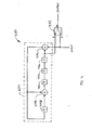
- FIG. 1 is a block diagram of a conventional circuit 100 that is used to generate CRC bits.
- circuit 100 generates a (7, 4) cyclic code.
- a (7, 4) cyclic code is a code that appends a three-bit codeword to four information bits thereby forming a group of seven total bits.
- G(x) has one high-order leading-zero term (i.e., the X 2 term is equal to zero).
- Circuit 100 includes a switch 102 and a linear feedback shift register (LFSR) 104.
- Switch 102 has three ports (a, b, and c).
- Switch 102 can be any conventional electronic switch such as, for example, any conventional type of field effect transistors (FET).
- FET field effect transistors
- LFSR 104 has three delay devices 106a, 106b, and 106c.
- LFSR 104 also has two adders 108a and 108b.
- Delay devices 106 can be any conventional type of delay device such as, for example, D-flipflops.
- Adders 108 represent modulo-2 addition and are implemented as exclusive-or circuits.
- LFSR 104 has two feedback loops. The innermost feedback loop is a nested feedback loop. This innermost nested feedback loop is formed by adders 108a and 108b, delay devices 106b and 106a, and the conductors coupling these devices together.
- Circuit 100 has two operating modes.
- a group of CRC bits or a CRC codeword (R 3 , R 2 , R 1 ) is generated by LFSR 104, wherein R 1 is output from delay device 106a, R 2 is output from delay device 106b, and R 3 is output from delay device 106c.
- the generated CRC codeword is shifted out of LFSR 104 and appended to a group of information bits.
- the a-port of switch 102 is electrically coupled to the b-port.
- bits of a digital information signal are input to the a-port of switch 102.
- a bit of the digital information signal is output at the b-port of switch 102.
- This same bit is also provided to adder 108a.
- the bit provided to adder 108a is added to an output of delay device 106a to form a resultant bit.
- This resultant bit is then provided as an input to adder 108b and to delay device 106c of LFSR 104.
- LFSR 104 is used to generate a CRC codeword for a group of four information signal bits (1, 1, 0, 1).
- each of the outputs of the delay devices 106 is a 0 bit (i.e., the codeword (R 3 , R 2 , R 1 ) of LFSR 104 is (0,0,0) before the first of four information signal bits (1, 1, 0, 1) is provided to circuit 100).
- the first bit of the four bits (1) is provided to the a-port of switch 102 and to adder 108a.
- This output bit (1) is then provided as an input to both delay device 106c and adder 108b.
- the second bit of the four bits (1) of the input signal is provided to the a-port of switch 102 and to adder 108a.
- clock cycle three the outputs of each of the delay devices 106 is again changed to that of their inputs, and the codeword (R 3 , R 2 , R 1 ) of LFSR 104 is changed from (1, 1, 0) to (1, 0, 1).
- the settling time of circuit 100 is equal to the settling time of two adders 108 (i.e., 2T adder ). This can be seen by noting that the output of adder 108b is dependent on the output of adder 108a. As illustrated by the circuit of FIG. 3, conventional unfolding techniques can increase this settling time of parallel CRC circuits since the critical paths of the unfolded circuits are typically longer than the sequential ones.
- circuit 100 In the second operating mode of circuit 100, the c-port rather than the a-port of switch 102 is electrically coupled to the b-port. In this second operating mode, during each clock cycle of circuit 100, a bit of a codeword generated by LFSR 104 is output at the b-port of switch 102.
- circuit 100 can be used to both generate CRC code words and append these code words to groups of bits of an information signal. For example, by switching to the second operating mode, the codeword (1, 0, 0) calculated during the transmission of the four information bits (1, 1, 0, 1) can be appended to the four information bits to form seven transmission bits (1, 1, 0, 1, 1, 0, 0).
- LFSR 104 includes two feedback loops. These feedback loops limit the rate at which data can be processed by circuit 100. Circuit 100 cannot be clocked any faster than the settling time of the slowest feedback loop.
- Unfolding is a technique for increasing the processing speed of certain digital circuits. Unfolding involves the formation of parallel processing paths. However, as described herein, conventional unfolding techniques can cause fan-out problems and increased circuit settling times. For this reason, conventional unfolding techniques cannot be used to design high speed digital communication systems, particularly systems intended to operate at a data rate in excess of 2 Gb/s.
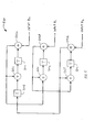
- FIG. 2 is a block diagram of a two parallel paths circuit 200 obtained by unfolding the LFSR 104 of circuit 100.
- circuit 200 has four adders 202a, 202b, 202c, and 202d and three delay devices 204a, 204b, and 204c.
- Circuit 200 can be used in lieu of LFSR 104 of circuit 100 to generate the code words of a (7, 4) CRC code.
- Circuit 200 generates a group of CRC bits or a CRC codeword (R 3 , R 2 , R 1 ), wherein R 1 is output from delay device 204a, R 2 is output from delay device 204b, and R 3 is output from delay device 204c.
- the iteration bound (settling time) of circuit 200 is equal to the settling time of two adders 202 (i.e., 2T adder ). This is due, for example, to the fact that the output of adder 202b is dependent on the output of adder 202a.
- Circuit 200 operates in a manner similar to that of circuit 100 except that two information bits are provided to circuit 200, rather than the one information of circuit 100, during each clock cycle of circuit 200.
- circuit 200 is used to generate a CRC codeword for a group of four information signal bits (1, 1, 0, 1). These are the same four information signal bits used above to illustrate the operation of LFSR 104.
- each of the outputs of the delay devices 204 is a 0 bit (i.e., the codeword (R 3 , R 2 , R 1 ) of circuit 200 is (0, 0, 0) before the first of four information signal bits (1, 1, 0, 1) is provided to circuit 200).
- the first bit of the four bits (1) is provided to adder 202a and the second bit of the four bits (1) is provided to adder 202d.
- the input to adder 202a is referred to as input B 0 .
- the second bit of the information signal (1) is provided as an input to adder 202d.
- This input to circuit 200 is referred to as input B 1 .
- This output bit is provided as an input bit to adder 202c and delay device 204c.
- clock cycle two the outputs of each of the delay devices 204 are changed to that of their inputs, and the codeword (R 3 , R 2 , R 1 ) of circuit 200 is changed from (0, 0, 0) to (1, 0, 1).
- the third bit of the four information bits (0) is provided to adder 202a.
- the fourth bit of the information signal (1) is provided as an input to adder 202d.
- circuit 200 generates the same codeword in two clock cycles as LFSR 104 generates in four clock cycles.
- the CRC code words generated by circuit 200 are appended to four information signal bits for transmission in a manner similar to that described above with regard to circuit 100.
- the circuit of FIG. 1 can be further unfolded in an attempt to further reduce processing time.
- further unfolding using conventional unfolding techniques can lead to increased circuit settling times and/or an inability to generate desired results.
- FIG. 3 is a block diagram of a three parallel paths circuit 300 obtained by unfolding the LFSR 104 of circuit 100.
- circuit 300 has six adders 302a, 302b, 302c, 302d, 302e, and 302f and three delay devices 304a, 304b, and 304c.
- Circuit 300 operates in a manner similar to that described above for circuit 200, and generates the codeword in two cycles. However, due to the increased unfolding, the setting time of the circuit is now equal to the settling time of four adders 302 (i.e., 4T adder ), which is double the setting time of circuit 200.
- FIG. 4 is a block diagram of a circuit 400 obtained by adding an additional time delay to the innermost nested feedback loop of the circuit 100 in accordance with the invention. Adding one or more additional time delays to the innermost nested feedback loop of a circuit prior to unfolding is a technique of the present invention. This technique of the invention is further described below. Adding one or more additional delays to the innermost nested feedback loop of a circuit prior to circuit unfolding allows the present invention to overcome the increased circuit settling time limitations associated with conventional unfolding techniques.
- Circuit 400 includes a switch 402 and a linear feedback shift register (LFSR) 404.
- Switch 402 has three ports (a, b, and c).
- LFSR 404 has four delay devices 406a, 406b, 406c, and 406d.
- LFSR 404 also has two adders 408a and 408b.
- the innermost nested feedback loop of LFSR 404 is formed by adder 408a, adder 408b, delay devices 406c, 406b and 406a, and the conductors coupling these devices together.
- Circuit 400 operates in a manner similar to that described above for circuit 100.
- P(x) has two high-order leading-zero term (i.e., the X 2 and the X 3 terms are equal to zero).
- the settling time of circuit 400 before unfolding is equal to the settling time of two adders 408 (i.e., 2T adder ). This can be seen by noting that the output of adder 408b is dependent on the output of adder 408a.
- FIG. 5 is a block diagram of a three parallel paths circuit 500 obtained by unfolding the LFSR 404 of circuit 400 in accordance with the invention. As shown in FIG. 5, circuit 500 has six adders 502a, 502b, 502c, 502d, 502e, and 502f and four delay devices 504a, 504b, 504c, and 504d.
- Circuit 500 is similar to that described above for circuit 300. However, the settling time of circuit 500 is equal to the settling time of two adders 502 (i.e., 2T adder ), which is the same as the setting time of circuit 400.
- the unfolding technique of the invention overcomes the limitations of conventional unfolding techniques.
- the unfolding technique of the invention is not limited by the example circuits illustrated herein.
- two additional time delays can be added to the innermost nested feedback loop of LFSR 104 such that each delay device 106a and 106b is effectively a 2T delay device.
- each of the delay devices 204a and 204b in circuit 200 would become a 2T delay device.
- additional time delays are added to the innermost nested feedback loop of LFSR 104 to permit increased unfolding in accordance with the invention and thereby increase the rate at which cyclic code words can be generated.
- the techniques of the present invention described above are used to form encoders for generating cyclic codes that are capable of operating at high data rates.
- FIG. 6A is a block diagram of an example encoder 600 according to the invention for generating the code words of a (7, 4) CRC code.
- Encoder 600 includes a first transform circuit 602, a LFSR 604, a second transform circuit 606 (which is another LFSR circuit), and a switch 608.
- Encoder 600 is different from circuit 100 in that it includes two transform circuits in addition to the LFSR 604, and LFSR 604 implements a different generator polynomial than LFSR 104.
- LFSR 104 implements the generator polynomial G(x) equals (1+X+X 3 ).
- G 2 (x) has two high-order leading-zero term (i.e., the X 3 and X 4 terms are equal to zero).
- the generator polynomial G 2 (x) is obtained by multiplying the generator polynomial G(x) equals (1+X+X 3 ) by the polynomial G 1 (x) equals (1+X 2 ).
- transform circuit 602 adds, using modulus-2 addition, the bits of a digital input signal U(x) to a copy of the digital input signal U(x) delayed by two time delays. This is equivalent to multiplying the bits of the digital input signal U(x) by the polynomial G 1 (x) equals (1+X 2 ), and it provides two degrees of look-ahead.
- Transform circuit 602 includes an adder 612a and two delay devices 610a and 610b.
- LFSR 604 operates in a manner similar to the devices described above with regard to LFSR 104.
- LFSR 604 implements a division operation and generates remained bits R 1 (x) at the output of a delay device 610c. These remainder bits are used to form a (7, 4) CRC code.
- LFSR 604 includes, in addition to delay device 610c, delay devices 610d, 610e, 610f, and 610g, and three adders 612b, 612c, and 612d.
- LFSR 604 divides the bits of the information signal U(x) by G 2 (x), wherein G 2 (x) equals G(x)G 1 (x).
- LFSR 604 is unfolded according to the invention to form three parallel processing paths and thereby increase the rate at which encoder 600 processes data.
- Transform circuit 606 transforms the remainder bits generated by LFSR 604 into the (7, 4) CRC code words generated by circuit 100. Transform circuit 606 adds the output signal generated at the output of delay device 610c by a delayed copy of this output signal. The delayed copy of the output signal is delayed by two time delays. Transform circuit 606 is equivalent to computing the quotient obtained by dividing the remainder bits generated by LFSR 604 by the polynomial G 1 (x) equals (1+X 2 ).
- Switch 608 operates similarly to switch 102 of circuit 100.
- Switch 608 can be any conventional electronic switch such as, for example, any conventional type of field effect transistors (FET).
- FET field effect transistors
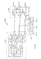
- FIG. 6B is a block diagram of an example three parallel paths circuit 650 according to the invention. Circuit 650 is obtained by unfolding circuit 600 by a factor of three.
- first transform circuit 602, LFSR 604, and second transform circuit 606 (which is another LFSR circuit) have each been unfolded in accordance with the invention.
- the unfolded first transform circuit 602 includes two delay devices 610 and three adders 612.
- the unfolded LFSR 604 includes five delay devices 610 and nine adders 612.
- the unfolded second transform circuit 606 includes two delay devices 610 and three adders 612.
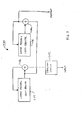
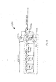
- FIG. 7 illustrates a simplified schematic of a second encoder 700 for generating a cyclic code according to an embodiment of the invention.
- Encoder 700 includes a transform circuit 702, a first LFSR 704, a second LFSR 706 and two modulo-2 adders 708a and 708b.
- the purpose of transform circuit 702 is to transform the bits of an information signal U(x) into the bits of a transformed information signal T(x).
- LFSR 704 implements a generator polynomial G 2 (x) formed by multiplying a conventional generator polynomial G(x) for implementing a particular cyclic code by a polynomial G 1 (x).
- the polynomial G 1 (x) is selected to increase the number of delays formed in the innermost nested feedback loop of LFSR 704.
- LFSR 704 may be unfolded/reformulated in accordance with the invention so as to avoid increasing the settling time (loop bound) of the unfolded/reformulated circuit.
- LFSR 706 implements a small degree polynomial used to transform the remained bits (code words) generated by LFSR 704 into the code words of a desired cyclic code (i.e., the code words that would typically be generated by the particular generator polynomial G(x) that was multiplied by the polynomial G 1 (x)). How to implement encoder 700 will become apparent to persons skilled in the relevant arts given the description of the invention herein.
- FIG. 8 is a block diagram of a second example LFSR circuit 800 for generating a cyclic code.
- This circuit can be derived from a circuit similar to circuit 100 (see FIG. 1) by retiming.
- Circuit 800 is used to generate the code words of a BCH code. As described below, the operation of circuit 800 is similar to the operation of circuit 100.
- FIG. 8 is provided as a second example circuit that can serve as a basis for making an encoder according to the invention.
- Other circuits for generating cyclic codes that can serve as a basis for making an encoder according to the invention will be known to persons skilled in the relevant arts given the description herein.
- circuit 800 includes three switches 802a, 802b and 802c, and an LFSR 804.
- LFSR 804 includes several delay devices 806 and several adders 808.
- Switch 802a has two ports (a and b).
- Switches 802b and 802c have three ports (a, b, and c).
- Switches 802 can be any conventional electronic switches such as, for example, any conventional type of field effect transistors (FET).
- Delay devices 806 can be any conventional type of delay devices such as, for example, D-flipflops.
- adders 808 can be any conventional type of modulo-2 adder circuits.
- LFSR 804 has several nested feedback loops.
- Delay device 806a forms a part of all of the nested feedback loops of LFSR 804.
- circuit 800 has two operating modes. In a first operating mode, a BCH codeword is generated by LFSR 804. In a second operating mode, the generated BCH codeword is shifted out of LFSR 804.
- the a-ports of switches 802a, 802b, and 802c are electrically coupled to the b-ports.
- two devices or nodes of a circuit are electrically coupled if a signal at one device or node of the circuit can be sensed at another device or node of the circuit.
- the sensed signal may be stored, filtered, and/or amplified, for example, before being sensed at another device or node of the circuit.
- bits of a digital information signal are input to the a-port of switch 802a.
- a bit of the digital information signal is output at the b-port of switch 802b. This same bit is also provided to adder 808a.
- the bit provided to adder 808a is added to an output of delay device 806a to form a resultant bit.
- This resultant bit is then provided as an input to each of the other adders 808 (e.g., adders 808b, 808c, and 808d) of LFSR 804 and to delay device 806d of LFSR 804.
- adders 808b, 808c, and 808d e.g., adders 808b, 808c, and 808d
- How LFSR loop 804 operates to generate a BCH codeword given a group of information signal bits would be known to a person skilled in the relevant arts given the description herein.
- the bits of the generated codeword are the outputs of each of the delay devices 806.
- the a-ports of switches 802a, 802b, and 802c are not electrically coupled to the b-ports.
- the c-port of switch 802b is electrically coupled to the b-port of switch 802b. Since the a-port of switch 802c is not electrically coupled to the b-port, the output of adder 808a is not fed back to any adder 808 or any delay device 806 of LFSR 804.
- a bit of the generated codeword is output at the b-port of switch 802b.
- a BCH encoder according to the invention has the form of encoder 700 described above.
- FIG. 9 and FIG. 10 illustrate how to apply the invention to retimed circuits.
- FIG. 9 illustrates an example embodiment of a LFSR circuit 900 that is equivalent to circuit 400 of FIG. 4.
- Circuit 900 is obtained by retiming circuit 400.
- FIG. 10 illustrates an example circuit 1000 according to the invention.
- Circuit 1000 is obtained by unfolding circuit 900 by a factor of three in accordance with the invention.
- Circuit 1000 illustrates how to apply the invention to retimed circuits such as, for example, the CRC circuits illustrated by FIG. 1 and FIG. 4.
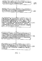
- FIG. 11 is a flowchart of the steps of a method 1100 for generating cyclic codes for error control in digital communications.
- method 1100 includes four steps 1102, 1104, 1106, and 1108.
- Method 1100 starts with step 1102.
- step 1102 a K-bit information signal is received.
- This information signal is represented by a polynomial U(x) having a degree K-1.
- the information signal U(x) is transformed to form a transformed information signal.
- the information signal U(x) is transformed using a first transform represented by a polynomial G 1 (x) having a degree P. P is greater than zero.
- the transformed information signal is represented by a polynomial T(x) having a degree K+P-1. T(x) equals U(x)G 1 (x).
- step 1104 involves adding the information signal U(x), using modulo-2 addition, to at least one time-shifted copy of the information signal to form the transformed information signal T(x).
- step 1104 can be implemented, for example, using the transform circuit 702 of circuit 700.
- step 1106 an initial cyclic code is generated for the transformed information signal T(x) using a second transform represented by a polynomial G 2 (x).
- This initial cyclic code is represented by a polynomial R 1 (x).
- G 2 (x) has high-order leading-zero terms.
- R 1 (x) equals the remainder obtained by dividing T(x) by G 2 (x).
- the K bits of the information signal U(x) are divided into at least two subsets of bits. These at least two subsets of bits are processed in parallel to generate the initial cyclic code R 1 (x).
- step 1106 can be implemented, for example, using the LFSR 704 of circuit 700.
- circuit 700 is unfolded in accordance with the invention to increase the rate at which data is processed.
- step 1108 the initial cyclic code R 1 (x) is transformed to form a final cyclic code represented by a polynomial R 2 (x).
- the initial cyclic code R 1 (x) is transformed using the first transform G 1 (x).
- R 2 (x) equals R 1 (x)/G 1 (x).
- the final cyclic code formed is a cyclic redundancy check code.
- the final cyclic code formed is a Bose-Chaudhuri-Hocquenghem code.
- the final cyclic code formed is a Reed-Solomon code.
- Other cyclic codes are also possible in accordance with the invention.
- step 1108 can be implemented, for example, using the LFSR 706 of circuit 700.
Landscapes
- Engineering & Computer Science (AREA)
- Physics & Mathematics (AREA)
- Theoretical Computer Science (AREA)
- General Physics & Mathematics (AREA)
- Mathematical Physics (AREA)
- Pure & Applied Mathematics (AREA)
- Probability & Statistics with Applications (AREA)
- Computing Systems (AREA)
- Computer Networks & Wireless Communication (AREA)
- Signal Processing (AREA)
- Algebra (AREA)
- Computational Mathematics (AREA)
- Mathematical Analysis (AREA)
- Mathematical Optimization (AREA)
- Power Engineering (AREA)
- Microelectronics & Electronic Packaging (AREA)
- Error Detection And Correction (AREA)
Applications Claiming Priority (2)
| Application Number | Priority Date | Filing Date | Title |
|---|---|---|---|
| US10/118,038 US6895545B2 (en) | 2002-01-28 | 2002-04-09 | System and method for generating cyclic codes for error control in digital communications |
| US118038 | 2002-04-09 |
Publications (3)
| Publication Number | Publication Date |
|---|---|
| EP1353446A2 true EP1353446A2 (fr) | 2003-10-15 |
| EP1353446A3 EP1353446A3 (fr) | 2004-03-17 |
| EP1353446B1 EP1353446B1 (fr) | 2006-07-12 |
Family
ID=28453960
Family Applications (1)
| Application Number | Title | Priority Date | Filing Date |
|---|---|---|---|
| EP03007893A Expired - Lifetime EP1353446B1 (fr) | 2002-04-09 | 2003-04-07 | Système et méthode pour générer des codes cycliques pour le contrôle d'erreurs pour des communications digitales |
Country Status (3)
| Country | Link |
|---|---|
| US (2) | US6895545B2 (fr) |
| EP (1) | EP1353446B1 (fr) |
| DE (1) | DE60306709T2 (fr) |
Cited By (3)
| Publication number | Priority date | Publication date | Assignee | Title |
|---|---|---|---|---|
| EP1612950A1 (fr) * | 2004-06-30 | 2006-01-04 | STMicroelectronics S.r.l. | Procédé et système pour corriger des erreurs pendant les opérations de lecture et d'écriture aux mémoires non-volatiles |
| RU2309537C1 (ru) * | 2006-04-07 | 2007-10-27 | ЗАО "Региональный научно-исследовательский экспертный центр" | Способ декодирования циклического помехоустойчивого кода |
| RU2435297C2 (ru) * | 2007-07-12 | 2011-11-27 | Самсунг Электроникс Ко., Лтд. | Способы и устройство для вычисления crc для множества кодовых блоков в системе связи |
Families Citing this family (7)
| Publication number | Priority date | Publication date | Assignee | Title |
|---|---|---|---|---|
| US7082563B2 (en) * | 2003-01-31 | 2006-07-25 | Italtel S.P.A. | Automated method for generating the cyclic redundancy check for transmission of multi-protocol packets |
| US8036380B2 (en) * | 2006-12-14 | 2011-10-11 | Telefonaktiebolaget L M Ericsson (Publ) | Efficient data integrity protection |
| US8464141B2 (en) | 2008-08-13 | 2013-06-11 | Infineon Technologies Ag | Programmable error correction capability for BCH codes |
| US8161434B2 (en) * | 2009-03-06 | 2012-04-17 | Synopsys, Inc. | Statistical formal activity analysis with consideration of temporal and spatial correlations |
| US8949703B2 (en) * | 2012-03-26 | 2015-02-03 | Xilinx, Inc. | Parallel encoding for non-binary linear block code |
| US11458909B2 (en) | 2020-02-06 | 2022-10-04 | Rosemount Aerospace Inc. | Adapter clip |
| TWI776483B (zh) * | 2021-04-26 | 2022-09-01 | 義守大學 | 循環碼之編碼與解碼方法 |
Family Cites Families (7)
| Publication number | Priority date | Publication date | Assignee | Title |
|---|---|---|---|---|
| US3703705A (en) * | 1970-12-31 | 1972-11-21 | Ibm | Multi-channel shift register |
| US5383204A (en) * | 1993-06-29 | 1995-01-17 | Mitsubishi Semiconductor America, Inc. | Parallel encoding apparatus and method implementing cyclic redundancy check and Reed-Solomon codes |
| AU4064697A (en) | 1996-08-15 | 1998-03-06 | Quantum Corporation | Parallel input ecc encoder and associated method of remainder computation |
| US5862159A (en) * | 1996-09-11 | 1999-01-19 | Texas Instruments Incorporated | Parallelized cyclical redundancy check method |
| US6519738B1 (en) * | 2000-03-07 | 2003-02-11 | International Business Machines Corporation | Method and apparatus for high-speed CRC computation based on state-variable transformation |
| US6934730B2 (en) * | 2000-10-13 | 2005-08-23 | Xpriori, Llc | Method and system for generating a transform |
| AU2003245898A1 (en) * | 2003-05-28 | 2005-01-21 | Telefonaktiebolaget L M Ericsson (Publ) | Parallel encoding of cyclic codes |
-
2002
- 2002-04-09 US US10/118,038 patent/US6895545B2/en not_active Expired - Fee Related
-
2003
- 2003-04-07 EP EP03007893A patent/EP1353446B1/fr not_active Expired - Lifetime
- 2003-04-07 DE DE60306709T patent/DE60306709T2/de not_active Expired - Lifetime
-
2005
- 2005-02-28 US US11/067,631 patent/US7539918B2/en not_active Expired - Fee Related
Cited By (5)
| Publication number | Priority date | Publication date | Assignee | Title |
|---|---|---|---|---|
| EP1612950A1 (fr) * | 2004-06-30 | 2006-01-04 | STMicroelectronics S.r.l. | Procédé et système pour corriger des erreurs pendant les opérations de lecture et d'écriture aux mémoires non-volatiles |
| RU2309537C1 (ru) * | 2006-04-07 | 2007-10-27 | ЗАО "Региональный научно-исследовательский экспертный центр" | Способ декодирования циклического помехоустойчивого кода |
| RU2435297C2 (ru) * | 2007-07-12 | 2011-11-27 | Самсунг Электроникс Ко., Лтд. | Способы и устройство для вычисления crc для множества кодовых блоков в системе связи |
| US8386878B2 (en) | 2007-07-12 | 2013-02-26 | Samsung Electronics Co., Ltd. | Methods and apparatus to compute CRC for multiple code blocks |
| US8862958B2 (en) | 2007-07-12 | 2014-10-14 | Samsung Electronics Co., Ltd. | Methods and apparatus to compute CRC for multiple code blocks |
Also Published As
| Publication number | Publication date |
|---|---|
| US6895545B2 (en) | 2005-05-17 |
| US20030154436A1 (en) | 2003-08-14 |
| DE60306709D1 (de) | 2006-08-24 |
| DE60306709T2 (de) | 2007-08-02 |
| US7539918B2 (en) | 2009-05-26 |
| US20050166122A1 (en) | 2005-07-28 |
| EP1353446B1 (fr) | 2006-07-12 |
| EP1353446A3 (fr) | 2004-03-17 |
Similar Documents
| Publication | Publication Date | Title |
|---|---|---|
| JP4355030B2 (ja) | 一般的なターボコードトレリスの終端方法およびシステム | |
| US4555784A (en) | Parity and syndrome generation for error detection and correction in digital communication systems | |
| US11804855B2 (en) | Pipelined forward error correction for vector signaling code channel | |
| US8108760B2 (en) | Decoding of linear codes with parity check matrix | |
| US8812940B2 (en) | Programmable error correction capability for BCH codes | |
| US7103830B1 (en) | DC balanced error correction coding | |
| US7219293B2 (en) | High performance CRC calculation method and system with a matrix transformation strategy | |
| KR101354288B1 (ko) | 통신 시스템에서 에러 검출 방법 및 장치 | |
| KR100659265B1 (ko) | 패리티비트가 역순으로 부가된 씨.알.씨. 코드의에러검출장치 및 방법 | |
| Parhi | Eliminating the fanout bottleneck in parallel long BCH encoders | |
| EP1353446A2 (fr) | Système et méthode pour générer des codes cycliques pour le contrôle d'erreurs pour des communications digitales | |
| US20050204268A1 (en) | Decoding and error correction for algebraic geometric codes | |
| US7320101B1 (en) | Fast parallel calculation of cyclic redundancy checks | |
| US7178091B1 (en) | Reed solomon encoder | |
| US20050066257A1 (en) | Parallelized CRC calculation method and system | |
| US20100031126A1 (en) | System and method for using the universal multipole for the implementation of a configurable binary bose-chaudhuri-hocquenghem (BCH) encoder with variable number of errors | |
| Panem et al. | Polynomials in Error Detection | |
| US8095848B1 (en) | Multi-byte cyclic redundancy check calculation circuit and method of operating the same | |
| Hajare et al. | Design and Implementation of Parallel CRC Generation for High Speed Application | |
| Kim | FPGA implementation of overhead reduction algorithm for interspersed redundancy bits using EEDC | |
| dos Santos | Insertion/deletion detection and bit-resynchronisation using the Viterbi algorithm | |
| Shanthi et al. | CHIPSCOPE Implementation of CRC circuit architecture | |
| Kaur et al. | VHDL IMPLEMENTATION OF UNIVERSAL LINEAR BLOCK ERROR DETECTOR AND CORRECTOR IN DIGITAL COMMUNICATION | |
| Boutros et al. | An efficient technique for detecting catastrophic convolutional codes |
Legal Events
| Date | Code | Title | Description |
|---|---|---|---|
| PUAI | Public reference made under article 153(3) epc to a published international application that has entered the european phase |
Free format text: ORIGINAL CODE: 0009012 |
|
| AK | Designated contracting states |
Kind code of ref document: A2 Designated state(s): AT BE BG CH CY CZ DE DK EE ES FI FR GB GR HU IE IT LI LU MC NL PT SE SI SK TR |
|
| AX | Request for extension of the european patent |
Extension state: AL LT LV MK RO |
|
| PUAL | Search report despatched |
Free format text: ORIGINAL CODE: 0009013 |
|
| AK | Designated contracting states |
Kind code of ref document: A3 Designated state(s): AT BE BG CH CY CZ DE DK EE ES FI FR GB GR HU IE IT LI LU MC NL PT SE SI SK TR |
|
| AX | Request for extension of the european patent |
Extension state: AL LT LV MK RO |
|
| RIC1 | Information provided on ipc code assigned before grant |
Ipc: 7H 03M 13/09 A Ipc: 7H 03M 13/15 B |
|
| 17P | Request for examination filed |
Effective date: 20040917 |
|
| 17Q | First examination report despatched |
Effective date: 20041018 |
|
| AKX | Designation fees paid |
Designated state(s): DE FR GB |
|
| GRAP | Despatch of communication of intention to grant a patent |
Free format text: ORIGINAL CODE: EPIDOSNIGR1 |
|
| GRAS | Grant fee paid |
Free format text: ORIGINAL CODE: EPIDOSNIGR3 |
|
| GRAA | (expected) grant |
Free format text: ORIGINAL CODE: 0009210 |
|
| AK | Designated contracting states |
Kind code of ref document: B1 Designated state(s): DE FR GB |
|
| REG | Reference to a national code |
Ref country code: GB Ref legal event code: FG4D |
|
| REF | Corresponds to: |
Ref document number: 60306709 Country of ref document: DE Date of ref document: 20060824 Kind code of ref document: P |
|
| ET | Fr: translation filed | ||
| PLBE | No opposition filed within time limit |
Free format text: ORIGINAL CODE: 0009261 |
|
| STAA | Information on the status of an ep patent application or granted ep patent |
Free format text: STATUS: NO OPPOSITION FILED WITHIN TIME LIMIT |
|
| RAP2 | Party data changed (patent owner data changed or rights of a patent transferred) |
Owner name: BROADCOM CORPORATION |
|
| 26N | No opposition filed |
Effective date: 20070413 |
|
| REG | Reference to a national code |
Ref country code: FR Ref legal event code: CA |
|
| PGFP | Annual fee paid to national office [announced via postgrant information from national office to epo] |
Ref country code: GB Payment date: 20130422 Year of fee payment: 11 |
|
| PGFP | Annual fee paid to national office [announced via postgrant information from national office to epo] |
Ref country code: FR Payment date: 20130523 Year of fee payment: 11 |
|
| PGFP | Annual fee paid to national office [announced via postgrant information from national office to epo] |
Ref country code: DE Payment date: 20140430 Year of fee payment: 12 |
|
| REG | Reference to a national code |
Ref country code: DE Ref legal event code: R119 Ref document number: 60306709 Country of ref document: DE |
|
| GBPC | Gb: european patent ceased through non-payment of renewal fee |
Effective date: 20140407 |
|
| REG | Reference to a national code |
Ref country code: DE Ref legal event code: R119 Ref document number: 60306709 Country of ref document: DE Effective date: 20141101 |
|
| REG | Reference to a national code |
Ref country code: FR Ref legal event code: ST Effective date: 20141231 |
|
| PG25 | Lapsed in a contracting state [announced via postgrant information from national office to epo] |
Ref country code: DE Free format text: LAPSE BECAUSE OF NON-PAYMENT OF DUE FEES Effective date: 20141101 Ref country code: GB Free format text: LAPSE BECAUSE OF NON-PAYMENT OF DUE FEES Effective date: 20140407 |
|
| PG25 | Lapsed in a contracting state [announced via postgrant information from national office to epo] |
Ref country code: FR Free format text: LAPSE BECAUSE OF NON-PAYMENT OF DUE FEES Effective date: 20140430 |