EP1353542A2 - Carte de circuit à couches multiples et méthode de sa production - Google Patents
Carte de circuit à couches multiples et méthode de sa production Download PDFInfo
- Publication number
- EP1353542A2 EP1353542A2 EP03014167A EP03014167A EP1353542A2 EP 1353542 A2 EP1353542 A2 EP 1353542A2 EP 03014167 A EP03014167 A EP 03014167A EP 03014167 A EP03014167 A EP 03014167A EP 1353542 A2 EP1353542 A2 EP 1353542A2
- Authority
- EP
- European Patent Office
- Prior art keywords
- glass
- metal element
- conductor layer
- converted
- dielectric
- Prior art date
- Legal status (The legal status is an assumption and is not a legal conclusion. Google has not performed a legal analysis and makes no representation as to the accuracy of the status listed.)
- Granted
Links
Images

Classifications
-
- C—CHEMISTRY; METALLURGY
- C03—GLASS; MINERAL OR SLAG WOOL
- C03C—CHEMICAL COMPOSITION OF GLASSES, GLAZES OR VITREOUS ENAMELS; SURFACE TREATMENT OF GLASS; SURFACE TREATMENT OF FIBRES OR FILAMENTS MADE FROM GLASS, MINERALS OR SLAGS; JOINING GLASS TO GLASS OR OTHER MATERIALS
- C03C4/00—Compositions for glass with special properties
- C03C4/16—Compositions for glass with special properties for dielectric glass
-
- C—CHEMISTRY; METALLURGY
- C03—GLASS; MINERAL OR SLAG WOOL
- C03C—CHEMICAL COMPOSITION OF GLASSES, GLAZES OR VITREOUS ENAMELS; SURFACE TREATMENT OF GLASS; SURFACE TREATMENT OF FIBRES OR FILAMENTS MADE FROM GLASS, MINERALS OR SLAGS; JOINING GLASS TO GLASS OR OTHER MATERIALS
- C03C8/00—Enamels; Glazes; Fusion seal compositions being frit compositions having non-frit additions
- C03C8/14—Glass frit mixtures having non-frit additions, e.g. opacifiers, colorants, mill-additions
-
- C—CHEMISTRY; METALLURGY
- C03—GLASS; MINERAL OR SLAG WOOL
- C03C—CHEMICAL COMPOSITION OF GLASSES, GLAZES OR VITREOUS ENAMELS; SURFACE TREATMENT OF GLASS; SURFACE TREATMENT OF FIBRES OR FILAMENTS MADE FROM GLASS, MINERALS OR SLAGS; JOINING GLASS TO GLASS OR OTHER MATERIALS
- C03C14/00—Glass compositions containing a non-glass component, e.g. compositions containing fibres, filaments, whiskers, platelets, or the like, dispersed in a glass matrix
- C03C14/004—Glass compositions containing a non-glass component, e.g. compositions containing fibres, filaments, whiskers, platelets, or the like, dispersed in a glass matrix the non-glass component being in the form of particles or flakes
-
- H—ELECTRICITY
- H05—ELECTRIC TECHNIQUES NOT OTHERWISE PROVIDED FOR
- H05K—PRINTED CIRCUITS; CASINGS OR CONSTRUCTIONAL DETAILS OF ELECTRIC APPARATUS; MANUFACTURE OF ASSEMBLAGES OF ELECTRICAL COMPONENTS
- H05K1/00—Printed circuits
- H05K1/02—Details
- H05K1/03—Use of materials for the substrate
- H05K1/0306—Inorganic insulating substrates, e.g. ceramic, glass
-
- H—ELECTRICITY
- H10—SEMICONDUCTOR DEVICES; ELECTRIC SOLID-STATE DEVICES NOT OTHERWISE PROVIDED FOR
- H10W—GENERIC PACKAGES, INTERCONNECTIONS, CONNECTORS OR OTHER CONSTRUCTIONAL DETAILS OF DEVICES COVERED BY CLASS H10
- H10W70/00—Package substrates; Interposers; Redistribution layers [RDL]
- H10W70/60—Insulating or insulated package substrates; Interposers; Redistribution layers
- H10W70/67—Insulating or insulated package substrates; Interposers; Redistribution layers characterised by their insulating layers or insulating parts
- H10W70/69—Insulating materials thereof
-
- C—CHEMISTRY; METALLURGY
- C03—GLASS; MINERAL OR SLAG WOOL
- C03C—CHEMICAL COMPOSITION OF GLASSES, GLAZES OR VITREOUS ENAMELS; SURFACE TREATMENT OF GLASS; SURFACE TREATMENT OF FIBRES OR FILAMENTS MADE FROM GLASS, MINERALS OR SLAGS; JOINING GLASS TO GLASS OR OTHER MATERIALS
- C03C2214/00—Nature of the non-vitreous component
- C03C2214/04—Particles; Flakes
-
- C—CHEMISTRY; METALLURGY
- C03—GLASS; MINERAL OR SLAG WOOL
- C03C—CHEMICAL COMPOSITION OF GLASSES, GLAZES OR VITREOUS ENAMELS; SURFACE TREATMENT OF GLASS; SURFACE TREATMENT OF FIBRES OR FILAMENTS MADE FROM GLASS, MINERALS OR SLAGS; JOINING GLASS TO GLASS OR OTHER MATERIALS
- C03C2214/00—Nature of the non-vitreous component
- C03C2214/30—Methods of making the composites
-
- H—ELECTRICITY
- H05—ELECTRIC TECHNIQUES NOT OTHERWISE PROVIDED FOR
- H05K—PRINTED CIRCUITS; CASINGS OR CONSTRUCTIONAL DETAILS OF ELECTRIC APPARATUS; MANUFACTURE OF ASSEMBLAGES OF ELECTRICAL COMPONENTS
- H05K1/00—Printed circuits
- H05K1/16—Printed circuits incorporating printed electric components, e.g. printed resistors, capacitors or inductors
- H05K1/162—Printed circuits incorporating printed electric components, e.g. printed resistors, capacitors or inductors incorporating printed capacitors
-
- H—ELECTRICITY
- H05—ELECTRIC TECHNIQUES NOT OTHERWISE PROVIDED FOR
- H05K—PRINTED CIRCUITS; CASINGS OR CONSTRUCTIONAL DETAILS OF ELECTRIC APPARATUS; MANUFACTURE OF ASSEMBLAGES OF ELECTRICAL COMPONENTS
- H05K3/00—Apparatus or processes for manufacturing printed circuits
- H05K3/46—Manufacturing multilayer circuits
- H05K3/4611—Manufacturing multilayer circuits by laminating two or more circuit boards
- H05K3/4626—Manufacturing multilayer circuits by laminating two or more circuit boards characterised by the insulating layers or materials
- H05K3/4629—Manufacturing multilayer circuits by laminating two or more circuit boards characterised by the insulating layers or materials laminating inorganic sheets comprising printed circuits, e.g. green ceramic sheets
-
- H—ELECTRICITY
- H05—ELECTRIC TECHNIQUES NOT OTHERWISE PROVIDED FOR
- H05K—PRINTED CIRCUITS; CASINGS OR CONSTRUCTIONAL DETAILS OF ELECTRIC APPARATUS; MANUFACTURE OF ASSEMBLAGES OF ELECTRICAL COMPONENTS
- H05K3/00—Apparatus or processes for manufacturing printed circuits
- H05K3/46—Manufacturing multilayer circuits
- H05K3/4644—Manufacturing multilayer circuits by building the multilayer layer by layer, i.e. build-up multilayer circuits
- H05K3/4673—Application methods or materials of intermediate insulating layers not specially adapted to any one of the previous methods of adding a circuit layer
- H05K3/4676—Single layer compositions
-
- Y—GENERAL TAGGING OF NEW TECHNOLOGICAL DEVELOPMENTS; GENERAL TAGGING OF CROSS-SECTIONAL TECHNOLOGIES SPANNING OVER SEVERAL SECTIONS OF THE IPC; TECHNICAL SUBJECTS COVERED BY FORMER USPC CROSS-REFERENCE ART COLLECTIONS [XRACs] AND DIGESTS
- Y10—TECHNICAL SUBJECTS COVERED BY FORMER USPC
- Y10T—TECHNICAL SUBJECTS COVERED BY FORMER US CLASSIFICATION
- Y10T428/00—Stock material or miscellaneous articles
- Y10T428/24—Structurally defined web or sheet [e.g., overall dimension, etc.]
- Y10T428/24802—Discontinuous or differential coating, impregnation or bond [e.g., artwork, printing, retouched photograph, etc.]
- Y10T428/24926—Discontinuous or differential coating, impregnation or bond [e.g., artwork, printing, retouched photograph, etc.] including ceramic, glass, porcelain or quartz layer
Definitions
- the present invention relates to a dielectric material and a dielectric sintered body, and to a wiring board using the same. More specifically, the invention relates to a dielectric material that can be sintered simultaneously with a conductor comprising a low-melting material such as Ag and Cu as a wiring board material and to a dielectric sintered body obtained by sintering the same. Particularly, the invention relates to a dielectric material having a low dielectric constant and superior high-frequency characteristics and having a wide width in optimum sintering conditions and to a dielectric sintered body obtained by sintering the same.
- the invention relates to a wiring board using this dielectric sintered body as a dielectric layer, which is suited for circuits having a high processing speed and high-frequency circuits.
- the wiring board according to the invention is widely used in high-frequency utilities such as packages for high-frequency MPU and packages of optical communication.
- the present invention also relates to a multilayered wiring board comprising a dielectric layer and a conductor layer, a part of the conductor layer being an entire electrode conductor layer having a forming area of 1 cm 2 or more, and a process of producing the same.
- the invention relates to a multilayered wiring board in which an entire electrode conductor layer is an ground electrode and/or a capacitor electrode and which is suitable for high-frequency applications having a strip line or micro-strip line.
- wiring boards are used in high-frequency regions having a frequency band in the order of GHz or more, with an increase in speed of information communication.
- the wiring boards are desired to use a metal having low conductor resistance, such as Ag and Cu, as a conductor layer thereof, thereby reducing a conductor loss.
- a metal having low conductor resistance such as Ag and Cu
- low temperature-sintering materials that can be sintered simultaneously with a low-melting metal such as Ag and Cu and that have superior high-frequency dielectric characteristics are being compared and investigated.
- crystallized glasses as a low temperature-sintering material having superior high-frequency characteristics, in which crystals having superior high-frequency characteristics crystallize during the sintering step.
- crystallized glasses there are, for example, known (1) crystallized glass of a spinel type crystal (for example, JP-A-9-175853(The term "JP-A” as used herein means an "unexamined published Japanese patent application")) , (2) crystallized glass of diopside (for example, JP-A-10-120436) , and (3) crystallized glass of alumina and anorthite (for example, JP-A-2000-143332).
- multilayered wiring boards that can realize relatively high-density wiring are widely used as wiring boards mounted with a semiconductor element such as LSI, IC, and discrete parts, or having a varied thick-film printing element incorporated therein.
- a semiconductor element such as LSI, IC, and discrete parts
- Most of these multilayered wiring boards are an alternate laminate of a dielectric layer comprising a glass ceramic and a conductor layer mainly composed of a metal conductor such as Cu, Ag, Au, W, and Mo, and if desired, a semiconductor element is mounted on the surface thereof.
- crystallized glasses are enumerated ones in which crystals of a spinel type structure are crystallized (JP-A-9-175853), ones in which crystals of diopside are crystallized (JP-A-10-120436), and ones in which crystals of alumina, etc. are crystallized (Japanese Patent Application No. 10-320612).
- a multilayered wiring board in which a part of the conductor layer is constituted as a strip line or micro-strip line (for example, JP-A-11-214812).
- a strip line or micro-strip line it is necessary to coat one surface of the dielectric layer substantially entirely and to form the entire electrode conductor layer, which functions as the ground conductor, as a part of the conductor layer.
- the entire electrode conductor layer is formed in a multilayered state inside the multilayered wiring board.
- the modulation of wiring boards there is a demand such that the entire electrode conductor layer is formed as a capacitor electrode, thereby forming a module wiring board with a built-in capacitor.
- the crystallized glass is once softened during the sintering step and thereafter loses fluidity with the progress of the crystallization. Accordingly, warp is liable to generate during the sintering step, and it is difficult to revise the warp by changing the sintering conditions. In contrast, in the case where a non-crystallized glass is used, such a problem hardly occurs. However, in the non-crystallized glass, though there is no problem in low-frequency regions of about 1 MHz, a dielectric loss often abruptly increases in high-frequency regions. Thus, it is not desired that the non-crystallized glass is used in the high-frequency regions.
- a first embodiment of the invention has been made and is aimed to provide a dielectric material having a wide width of sintering conditions, in which a dielectric sintered body after sintering has both characteristics of a low dielectric constant and a low dielectric loss and to provide a dielectric sintered body. Further, the first embodiment of the invention is aimed to provide a dielectric material that can undergo degreasing with a good efficiency, thereby stably obtaining a dielectric sintered body and a dielectric sintered body, and to provide a wiring board using the same.
- the dielectric material according to the first embodiment of the invention comprises a glass powder constituted of a glass containing Si, B and an alkali metal element, the glass being amorphous in sintering at a temperature of 1,050 °C or lower; and a ceramic filler containing at least one member of SiO 2 , Al 2 O 3 and 3Al 2 O 3 ⁇ 2SiO 2 , and an alkali metal element, wherein when the total sum of Si converted into SiO 2 , B converted into B 2 O 3 and the alkali metal element converted into A 2 O, wherein A represents an alkali metal element, all of which are contained in the glass, is 100 mole %, a content of the alkali metal element converted into A 2 O, which is contained in the glass, is 0.5 mole % or less; and when the total sum of at least one member of SiO 2, Al 2 O 3 and 3Al 2 O 3 ⁇ 2SiO 2 , and the alkali metal element converted into A 2 O, all of which are
- Another dielectric material according to the first embodiment of the invention comprises a glass powder constituted of a glass containing Si, B and an alkali metal element, the glass being amorphous in sintering at a temperature of 1,050 °C or lower; and a ceramic filler containing at least one member of SiO 2 , Al 2 O 3 and 3Al 2 O3 ⁇ 2SiO 2 but not containing an alkali metal element, wherein when the total sum of Si converted into SiO 2 , B converted into B 2 O 3 and the alkali metal element converted into A 2 O, wherein A represents an alkali metal element, all of which are contained in the glass, is 100 mole %, a content of the alkali metal element converted into A 2 O, which is contained in the glass, is 0.5 mole % or less.
- the glass can further contain Al and/or an alkaline earth metal element, and when the total sum of Si converted into SiO 2 , B converted into B 2 O 3 , the alkali metal element converted into A 2 O, wherein A represents an alkali metal element, Al converted into Al 2 O 3 in the case where Al is contained, and the alkaline earth metal element converted into EO, wherein E represents an alkaline earth metal element, in the case where the alkaline earth metal element is contained, is 100 mole %, the total sum of Si converted into SiO 2 and B converted into B 2 O 3 is from 80 to 95 mole %.
- the ceramic filler may not contain an alkaline earth metal element.
- the ceramic filler can further contain an alkaline earth metal element, and when the total sum of at least one member of SiO 2 , Al 2 O 3 and 3Al 2 O 3 ⁇ 2SiO 2 , the alkali metal element converted into A 2 O, in the case where the alkali metal element is contained, and the alkaline earth metal element converted into EO, wherein E represents an alkaline earth metal element, all of which are contained in the ceramic filler, is 100 mole %, a content of the alkaline earth metal element converted into EO is 1 mole % or less.
- the glass powder can account for from 55 to 70 % by volume, and the ceramic filler can account for from 30 to 45 % by volume.
- the dielectric sintered body according to the first embodiment of the invention is one obtained by sintering the dielectric material, wherein when the total sum of Si converted into SiO 2 , B converted into B 2 O 3 , the alkali metal element converted into A 2 O, wherein A represents an alkali metal element, Al converted into Al 2 O 3 in the case where Al is contained, and the alkaline earth metal element converted into EO, wherein E represents an alkaline earth metal element, in the case where the alkaline earth metal element is contained, all of which are contained in the glass, is 100 mole %, and at least one member of SiO 2 , Al 2 O 3 and 3Al 2 O 3 ⁇ 2SiO 2 , the alkali metal element converted into A 2 O, in the case where the alkali metal element is contained, and the alkaline earth metal element converted into EO, wherein E represents an alkaline earth metal element, all of which are contained in the ceramic filler, is 100 mole %, a content of the alkali metal element converted
- the wiring board according to the first embodiment of the invention comprises a dielectric layer comprising the dielectric sintered body and a conductor layer provided on the surface of or inside the dielectric layer, the conductor layer comprising at least one member selected from Ag, Au and Cu.
- Electrode layer a conductor layer containing the entire electrode conductor layer (hereinafter sometimes abbreviated as "electrode layer”) and a dielectric layer using the crystallized glass are simultaneously sintered to prepare a multilayered wiring board (second embodiment of the invention), as shown in a schematic view of Fig. 4, there is a problem that a blister or gap is liable to generate due to differences in the sintering temperature and sintering shrinkage behavior between the dielectric layer and the conductor layer. This is because since the crystallized glass has a nature such that it is abruptly sintered and shrunk during the sintering step, the sintering shrinkage behavior of the entire electrode conductor layer cannot follow it.
- Such a blister or gap is liable to generate in the entire electrode conductor layer (forming area: 1 cm 2 or more) having a large contact area with the dielectric layer.
- the generation of such a blister or gap results in inconveniences such as reduction in mechanical strength due to reduction of adhesiveness between the conductor layer and the dielectric layer and increase of the resistivity. Further, these inconveniences become remarkable when the entire electrode conductor layer is formed in a multilayered state in the multilayered wiring board.
- the blister or gap generated in the electrode layer occurs due to a difference of the shrinkage behavior caused by differences in the sintering temperature and sintering shrinkage behavior between the dielectric layer and the conductor layer during the sintering.
- it is attempted to regulate the amount of the metal conductor component mainly constituting the conductor layer or to add a metal conductor different from the metal conductor mainly constituting the conductor layer to the conductor layer.
- JP-A-63-168904 and JP-A-62-48097 propose such devices.
- the sintering be carried out at a sintering temperature lower than the melting point of the metal, namely, at a low sintering temperature of from 800 to 1,050 °C. Accordingly, the sintering temperature region at which the simultaneous sintering with the dielectric layer can be carried out is limited depending on the species of the metal constituting the conductor layer.
- the dielectric layer is required to have a low specific dielectric constant and a low dielectric loss, suited for the high-frequency signal.
- the sintering temperature region will be made narrower.
- the mere device on the constitutional components of the conductor layer as in the related art it becomes more difficult to inhibit the inconveniences generated in the electrode layer without worsening the electric characteristics such as resistivity in the conductor layer.
- the width of optimization of the sintering conditions such as sintering temperature is as wide as possible.
- the sintering is carried out in a neutral atmosphere or reductive atmosphere. For this reason, in particular, it is preferred that the width of optimization of the sintering conditions is as wide as possible.
- the dielectric layer is sintered and formed in a state where besides the constitutional components, a binder that is usually composed of an organic material is contained, or a state where debinding is effected in advance to some extent.
- the binder is degreased and removed in the sintering stage or debinding stage in advance.
- the sintering is carried out in a state where the debinding is incomplete, the constitutional components forming the dielectric layer become minute before the binder has completely come out, whereby a passage through which the binder comes out is clogged, leading to a problem such that the debinding becomes difficult.
- the width of optimization of the sintering conditions in the simultaneous sintering is as wide as possible.
- an object of the second embodiment of the invention is to provide a wiring board in which even in the case where the dielectric layer and the conductor layer are simultaneously sintered, not only inconveniences such as blister generated between the conductor layer (especially, the entire electrode conductor layer having a forming area of 1 cm 2 or more) and the dielectric layer are inhibited, but also electric characteristics represented by resistivity of the conductor layer to be formed can be enhanced, especially the dielectric layer and the conductor layer suited for high-frequency signals can be formed, and the productivity can be enhanced, and to provide a process of producing the same.
- the multilayered wiring board according to the second embodiment of the invention comprises a dielectric layer constituted of a glass having a crystallization temperature exceeding 1,000 °C and a ceramic filler and a conductor layer mainly constituted of a metal conductor, wherein a part of the conductor layer is constituted as an entire electrode conductor layer having a forming area of 1 cm 2 or more.
- the glass that is the raw material of the glass matrix constituting the dielectric layer one having a crystallization temperature exceeding 1,000 °C is used. Accordingly, in the case where the dielectric layer is sintered simultaneously with the conductor layer mainly constituted of a low-melting metal conductor such as Ag and Cu by sintering at from 800 to 1,000 °C, the glass matrix constituting the dielectric layer can be formed as one in which the crystallization is inhibited during the sintering or one in which no crystallization occurs. For this reason, it is possible to inhibit the difference in shrinkage behavior caused by the particles of the constitutional components of the dielectric layer and the conductor layer during the sintering.
- electrode layer the entire electrode conductor layer having a forming area of 1 cm 2 or more (hereinafter sometimes simply referred to "electrode layer"), which constitutes a part of the conductor layer. Furthermore, it is possible to enhance the electric characteristics of the conductor layer, such as resistivity.
- the dielectric layer is formed by using a glass in which the crystallization is inhibited during the sintering step, or a glass in which no crystallization occurs, it is possible to widen the width of the sintering conditions such as the sintering temperature for simultaneous sintering of the dielectric layer and the conductor layer. Furthermore, it is possible to enhance the productivity of the multilayered wiring board to be formed.
- the crystallization temperature of the glass to be used in the second embodiment of the invention is as high as possible.
- what the crystallization of the glass is inhibited during the sintering means that the crystallization of the glass does not substantially occur during the time when the dielectric layer becomes minute.
- the glass is crystallized by a post-treatment (for example, prolonging the holding time at the sintering temperature) after the dielectric layer has become minute should be included in the concept of the dielectric layer of the second embodiment of the invention. Further, even in the case where after the dielectric layer has become minute, the glass is crystallized, since the simultaneous sintering of the dielectric layer and the conductor layer is already completed, warp caused by mismatching of the sintering shrinkage does not occur.
- a post-treatment for example, prolonging the holding time at the sintering temperature
- the metal conductor mainly constituting the conductor layer in the multilayered wiring board according to the second embodiment of the invention is of a low resistivity.
- the resistivity of the conductor layer is low.
- a metal conductor can be enumerated silver-based conductors (such as silver alone, silver-metal oxide (oxides of, e.g., manganese, vanadium, bismuth, aluminum, silicon, copper (hereinafter simply referred to as "metal oxide")), silver-glass, silver-palladium, silver-platinum, and silver-rhodium), gold-based conductors (gold alone, gold-metal oxide, gold-palladium, gold-platinum, and gold-rhodium), and copper-based conductors (such as copper alone, copper-metal oxide, copper-palladium, copper-platinum, and copper-rhodium).
- silver-based conductors such as silver alone, silver-metal oxide (oxides of, e.g., manganese, vanadium, bismuth, aluminum, silicon, copper (hereinafter simply referred to as "metal oxide")
- silver-glass silver-palladium, silver-platinum, and silver-r
- Cu, Ag and Au are of a low resistivity. Accordingly, those mainly composed of Cu or Ag are suitable as the metal conductor mainly constituting the conductor layer. Especially, those mainly composed of Cu that is superior in anti-migration to Ag are suitable as the metal conductor mainly constituting the conductor layer. Further, in the second embodiment of the invention, since the dielectric layer is sintered at from 800 to 1,000 °C using the glass having a crystallization temperature exceeding 1,000 °C, sintering proceeds slowly as compared with the case of using a glass having a low crystallization temperature.
- the multilayered wiring board according to the second embodiment of the invention is characterized in that the entire electrode conductor layer is an ground electrode and/or a capacitor electrode.
- the ground electrode that is necessary in the case where a part of the conductor layer functions a strip line or a micro-strip line, or the capacitor electrode that is necessary in the case where a capacitor (including known capacitors such as laminate type capacitors in the concept) is built in the multilayered wiring board corresponding to high-frequency signals, is not only formed as a part of the conductor layer but also has a forming area as large as possible, i.e., a forming area of at least 1 cm 2 .
- Such ground electrode and capacitor electrode correspond to the entire electrode conductor layer.
- the dielectric layer is sintered while inhibiting the crystallization during the sintering, it is possible to inhibit the blister or gap that is conventionally generated in the conductor layer, especially the entire electrode conductor layer (forming area: 1 cm 2 or more) due to the difference in abrupt shrinkage behavior with the progress of crystallization of the crystallized glass during the sintering.
- the entire electrode conductor layer functioning as the ground electrode or capacitor electrode can have a forming area of at least 1 cm 2 .
- the electrode layer is formed in a multilayered state inside the multilayered wiring board, it is possible to inhibit effectively the blister or gap generated in the electrode layer.
- the conductor layer can have a volume resistivity of 4 x 10 -6 ⁇ cm or less (particularly 3 x 10 -6 ⁇ cm or less, and further particularly 2.5 x 10 -6 ⁇ cm or less) .
- the conductor layer can have a volume resistivity of 4 x 10 -6 ⁇ cm or less (particularly 3 x 10 -6 ⁇ cm or less, and further particularly 2.5 x 10 -6 ⁇ cm or less) .
- the specific dielectric constant and the dielectric loss of the dielectric layer are as low as possible.
- the specific dielectric constant may be 7 or less, and the dielectric loss in a high high-frequency band of 10 GHz or more may be 0.002 or less.
- the glass as a constitutional component of the dielectric layer can comprise SiO 2 and B 2 O 3 as major components and Al 2 O 3 and an alkaline earth metal oxide as sub-components, with a content of the major components being from 80 to 95 mole %.
- the glass consists essentially of SiO 2 and B 2 O 3 as major components and Al 2 O 3 and an alkaline earth metal oxide as sub-components. More preferably, the glass consists of SiO 2 and B 2 O 3 as major components and Al 2 O 3 and an alkaline earth metal oxide as sub-components.
- the glass comprising such components, even when the crystallization temperature exceeds 1,000 °C, and the sintering is carried out at from 800 to 1,000 °C, the glass is not crystallized. Accordingly, it is possible to relieve effectively the mismatching of the sintering shrinkage behavior during the simultaneous sintering with the metal conductor such as Cu.
- the content of SiO 2 and B 2 O 3 (hereinafter sometimes abbreviated as "major components") as the major components of the glass is from 80 to 95 mole %.
- major components When the content of the major components exceeds 95 mole %, crystals caused by SiO 2 , such as cristobalite, exist in the sintering step (sintering temperature: 1,000 °C or lower).
- the content of the major components is less than 80 mole%, there occur inconveniences such that the specific dielectric constant or dielectric loss in a high-frequency band of the formed dielectric layer becomes high. Taking into consideration these matters, it is desired that the content of the major components is from 80 to 95 mole %.
- Al 2 O 3 and an alkaline earth metal oxide as sub-components of the glass have an effect for inhibiting the crystallization caused by the major components in the sintering step, and desirably, the content of each of Al 2 O 3 and the alkaline earth metal oxide is from 3 to 10 mole %.
- the content of Al 2 O 3 is less than 3 mole %, crystals caused by SiO 2 exist in the sintering step.
- the content of Al 2 O 3 exceeds 10 mole %, there occur inconveniences such that Al 2 O 3 crystals and faldspar caused by Al 2 O 3 exist in the sintering step. Taking into consideration these matters, it is suitable that the content of Al 2 O 3 in the glass is from 3 to 10 mole %.
- the content of the alkaline earth metal oxide is less than 3 mole %, the melting of the glass as the major components in the sintering step becomes difficult.
- it exceeds 10 mole % there occur inconveniences such that crystals caused by the alkaline earth metal oxide exist in the sintering step. Taking into consideration these matters, it is desired that the content of the alkaline earth metal oxide is from 3 to 10 mole %.
- the alkaline earth metal oxide can be enumerated MgO, CaO, SriO, and BaO.
- MgO is liable to cause crystallization in the sintering step, and SrO and Bao excessively increase the specific dielectric constant of the formed dielectric layer. Therefore, it is particularly optimum to choose CaO.
- CaO is chosen as the alkaline earth metal oxide, not only it is possible to easily inhibit the generation of crystallization caused by the constitutional components of the glass during the sintering, but also it becomes possible to reduce the specific dielectric constant of the dielectric layer.
- the formation of oxides caused by these metal components in the sintering step increases the dielectric loss of the dielectric layer in a high-frequency band.
- the second embodiment of the invention it is possible to sinter and form the dielectric layer by sintering at 1,000 °C or lower without containing alkali metals and metal components such as Pb and Sb in the glass powder. As a result, it is possible to inhibit inconveniences such as an increase of the dielectric loss in a high-frequency band by the oxides caused by the metal components. Furthermore, it is possible to further reduce the dielectric loss of the formed dielectric layer in a high-frequency band.
- the entire electrode conductor layer in addition to the function of an ground conductor of, e.g., a strip line corresponding to high-frequency signals, there may be the case where the entire electrode conductor layer is formed as an ground conductor as a shield portion for noise protection irrespective of the frequency of high-frequency signals. Even in such case, as described in the second embodiment of the invention, it is possible to inhibit inconveniences such as blister or gap as generated during the sintering.
- the process of producing the multilayered wiring board according to the second embodiment of the invention comprises sintering a multilayered wiring board molding comprising a green material mainly constituted of a glass having a crystallization temperature exceeding 1,000 °C and a ceramic filler and a conductor layer mainly constituted of a metal conductor, a part of the conductor layer being constituted as an entire electrode conductor layer having a forming area of 1 cm 2 or more, at a temperature lower than the crystallization temperature of the glass.
- the crystallization temperature of the glass constituting the green material that will be the dielectric layer by sintering exceeds 1,000 °C, even in the case where simultaneous sintering with the conductor layer mainly composed of a metal conductor having a low melting point, such as Ag and Cu, is carried out by sintering at from 800 to 1,000 °C, it is possible to form the glass constituting the dielectric layer as a glass in which the crystallization is inhibited during the sintering, or a glass in which no crystallization occurs. For this reason, it is possible to inhibit the difference in shrinkage behavior caused in particles of the constitutional components between the dielectric layer and the conductor layer during the sintering.
- the dielectric layer and the conductor layer are subjected to simultaneous sintering, it is possible to inhibit the inconveniences such as blister and peeling generated in the conductor layer, especially the entire electrode conductor layer having a forming area of 1 cm 2 or more, which constitutes a part of the conductor layer. Furthermore, it is possible to produce a multilayered wiring board, namely a multilayered wiring board, having enhanced electric characteristics of the conductor layer, such as resistivity.
- the glass constituting the green material is a glass in which the crystallization is inhibited during the sintering step, or a glass in which no crystallization occurs, it is possible to widen the width of the sintering conditions such as the sintering temperature for simultaneous sintering of the dielectric layer and the conductor layer. As a result, by widening the width of the sintering conditions, it is possible to enhance the debinding properties of a binder comprising an organic material, which is contained in the green material, in the sintering step.
- the multilayered wiring board produced by the production process according to the second embodiment of the invention has the same effects as in the above-described multilayered wiring board according to the second embodiment of the invention.
- the dielectric layer has a specific dielectric constant of 7 or less and a dielectric loss of 0.002 or less in a high-frequency band of 10 GHz or more
- the glass powder in the production process according to the second embodiment of the invention have SiO 2 and B 2 O 3 as major components and Al 2 O 3 and an alkaline earth metal oxide as sub-components, with a content of the major components being from 80 to 95 mole %.
- the dielectric material (one before sintering, which is hereinafter sometimes simply referred to as "material") according to the first embodiment of the invention contains a glass powder and a ceramic filler.
- the glass powder preferably has a mean particle size of from 0.5 to 5 ⁇ m, and more preferably from 1 to 3 ⁇ m.
- the "glass powder” is constituted of a glass containing Si, B and an alkali metal element, the glass being amorphous. in sintering at a temperature of 1,050 °C or lower.
- amorphous means that no peak is confirmed in the X-ray diffraction. That is, it can be confirmed whether or not the "glass” is amorphous by the matter that when the glass powder is sintered at 1,050 °C for 2 hours and then subjected to X-ray diffraction measurement, no peak is present in the X-ray diffraction.
- Si and B are contained means that the glass is constituted of a borosilicate glass. Accordingly, these are contained mainly as oxides of Si and B.
- examples of the alkali metal element that is contained in the glass include Li, Na, and K. Still further, the alkali metal element is contained usually as its oxide. Also, the alkali metal element may be contained singly or in admixture of two or more thereof.
- Si converted into oxide B converted into B 2 O 3
- alkali metal element converted into A 2 O alkali metal element converted into oxide
- A represents an alkali metal element
- a content of the alkali metal element converted into A 2 O, which is contained in the glass is 0.5 mole % or less, preferably 0.3 mole % or less, and more preferably 0.2 mole % or less.
- what the total sum of Si, B and the alkali metal element (A) each converted into oxide is 100 mole % means that the total sum of Si converted into SiO 2 , B converted into B 2 O 3 and A converted into A 2 O is 100 mole % but does not mean mole % of Si, B and the alkali metal element contained in the oxides.
- the mole % of "B converted into B 2 O 3 " is 10 mole % but not the mole % of "B contained in B 2 O 3 " (namely, 20 mole %).
- This glass preferably has a yielding point of from 700 to 850 °C, and more preferably from 720 to 800 °C.
- the yielding point is lower than 700 °C, it is difficult to remove carbon generated from a binder during the sintering.
- the sintering temperature is too high, so that it becomes difficult to undergo the sintering simultaneously with metals such as Au, Ag, and Cu, and hence, such is not preferred.
- the glass is not particularly limited so far as it is a borosilicate glass that is amorphous in the sintering at 1,050 °C or lower. But, it may further contain Al and/or an alkaline earth metal element.
- the total sum of Si converted into oxide, B converted into oxide, the alkali metal element converted into oxide, Al converted into Al 2 O 3 (hereinafter referred to as "Al converted into oxide") in the case where Al is contained, and the alkaline earth metal element converted into EO (hereinafter referred to as "alkaline earth metal element converted into oxide), wherein E represents an alkaline earth metal element (hereinafter the same), in the case where the alkaline earth metal element is contained, all of which are contained in the glass, is 100 mole %
- the total sum of Si and B each converted into oxide is preferably from 80 to 95 mole %, more preferably from 82 to 93 mole %, and most preferably from 85 to 90 mole %.
- the content of Al converted into oxide is preferably from 3 to 10 mole %.
- the content of Al converted into oxide is less than 3 mole %, SiO 2 -based crystals are liable to crystallize during the sintering, whereas when it exceeds 10 mole %, Al 2 O 3 -based crystals or faldspar is liable to crystallize during the sintering, and hence, the both are not preferred.
- alkaline earth metal element examples include Ca, Mg, Sr, and Ba
- Ca is particularly preferred.
- Mg is liable to crystallize Mg-based crystals such as enstatite and cordierite during the sintering
- Sr and Ba are liable to increase the dielectric constant of the dielectric sintered body after the sintering, and hence, the both are not preferred.
- the content of the alkaline earth metal element converted into oxide is preferably from 3 to 10 mole %.
- the content of the alkaline earth metal element converted into oxide is less than 3 mole %, melting of the glass is difficult, whereas when it exceeds 10 mole %, crystals are liable to crystallize during the sintering, and hence, the both are not preferred.
- the "ceramic filler” means one containing at least one member of SiO 2 , Al 2 O 3 and 3Al 2 O 3 ⁇ 2SiO 2 (mullite).
- the ceramic filler may be one containing an alkali metal element, those not containing an alkali metal element are preferred. This is because in the case where the alkali metal element is contained, an increase of dielectric loss of the dielectric sintered body after the sintering is liable to occur.
- the alkali metal element is not contained means that in the chemical analysis (ICP emission), its detection amount is smaller than the measurement limit.
- the alkali metal element when the total sum of at least one member of SiO 2 , Al 2 O 3 and 3Al 2 O 3 ⁇ 2SiO 2 and the alkali metal element converted into oxide, all of which are contained in the ceramic filler, is 100 mole %, the content of the alkali metal element converted into oxide is 0.5 mole % or less, preferably 0.3 mole % or less, and more preferably 0.2 mole % or less.
- the content of the alkali metal element converted into oxide exceeds 0.5 mole %, the dielectric loss of the dielectric sintered body after the sintering becomes large, and hence, such is not preferred.
- the ceramic filler may be one containing an alkaline earth metal element, those not containing an alkaline earth metal element are preferred. This is because in the case where the alkaline earth metal element is contained, an increase of dielectric loss of the dielectric sintered body after the sintering is liable to occur.
- what the alkaline earth metal element is not contained means that in the chemical analysis (ICP emission), its detection amount is smaller than the measurement limit.
- the alkali metal element converted into oxide in the case where the alkali metal element is contained, and the alkaline earth metal element converted into oxide, all of which are contained in the ceramic filler is 100 mole %
- the content of the alkaline earth metal element converted into oxide is 1 mole % or less, preferably 0.5 mole % or less, and more preferably 0.2 mole % or less.
- the content of the alkali metal element converted into oxide exceeds 1 mole %, the dielectric loss of the dielectric sintered body after the sintering becomes large, and hence, such is not preferred.
- the ceramic filler may be in a powdered state or fibrous state, but preferably is in a powdered state. In the case where the ceramic filler is in a powdered state, it preferably has a mean particle size of from 0.5 to 5 ⁇ m, and more preferably from 1 to 3 ⁇ m.
- the ceramic filler examples include an alumina powder, a mullite powder, a quartz powder, and a silica glass powder.
- the alumina powder is preferred because it can enhance the strength of the dielectric sintered body.
- these ceramic fillers may be used singly or in admixture of two or more thereof depending upon the dielectric constant, strength and coefficient of thermal expansion required for the dielectric sintered body. Further, in the case where two or more of the ceramic fillers are used in combination, ones having an alumina powder mixed therewith are preferred because they can enhance the strength of the dielectric sintered body after the sintering.
- the glass powder accounts for from 55 to 70 % by volume, and the ceramic filler accounts for from 30 to 70 % by volume, and it is more preferred that the glass powder accounts for from 55 % by volume or more but less than 65 % by volume, and the ceramic filler accounts for more than 35 % by volume but 45 % by volume or less.
- the amount of the glass powder is less than 55 % by volume, a minute sintered body is hardly obtained during the sintering, whereas when it exceeds 70 % by volume, the debinding properties are lowered, and hence, the both are not preferred.
- % by volume means a volume ratio in a true volume, and the true volume of each of the glass powder and the ceramic filler is determined by dividing a weight of each powder by a particle density of each powder.
- the particle density of the powder can be measured by known methods (such as the pycnometer method of JIS R 1620 "Testing Method for Particle Density of Fine Ceramic Powder”).
- the dielectric material according to the first embodiment of the invention is usually obtained by compounding the glass powder and the ceramic filler further with at least a solvent and a binder.
- the binder is not particularly limited so far as it is generally used as a binder. But, acrylic resin-based binders such as acrylic resins and butyral resins are preferred, and acrylic resins are particularly preferably used.
- the binder may be used singly or in admixture of two or more thereof.
- a compounding amount of the binder is from 1 to 30 parts by weight, and preferably from 3 to 25 parts by weight.
- the solvent is not particularly limited so far as it is a solvent generally used for dielectric materials. But, examples include toluene, methyl ethyl ketone, acetone, and isopropyl alcohol. Of these are preferable toluene and methyl ethyl ketone.
- the solvent may be used singly or in admixture of two or more thereof.
- a compounding amount of the solvent is from 10 to 150 parts by weight, and preferably from 20 to 120 parts by weight.
- the dielectric material according to the first embodiment of the invention may be further compounded with a plasticizer. Such compounding is carried out for the purpose of enhancing the processing properties of a green sheet.
- plasticizer examples include dibutyl phthalate, 2-ethylhexyl phthalate, and 2-ethylhexyl adipate, with dibutyl phthalate being preferred.
- the plasticizer may be used singly or in admixture of two or more thereof.
- a compounding amount of the plasticizer is from 3 to 20 parts by weight, and preferably from 5 to 15 parts by weight.
- the dielectric sintered body according to the first embodiment of the invention is obtained by sintering the dielectric material.
- the dielectric sintered body is obtained from the dielectric material according to the first embodiment of the invention, it is usually carried out to mold the dielectric material prior to the sintering.
- the molding can be carried out by known molding methods represented by sheet molding by the doctor blade process (including a laminate of plural sheets) , film formation by the screen printing process, and press molding.
- the sintering is carried out at from 800 to 1,050 °C, and preferably from 900 to 1,000 °C for from 0.5 to 10 hours, and preferably from 1 to 5 hours.
- the sintering temperature is lower than 800 °C, sufficient sintering is hardly achieved, whereas when it exceeds 1,050 °C, growth of metallized abnormal particles (Cu) to be simultaneously sintered occurs, and hence, the both are not preferred.
- the sintering time is shorter than 0.5 hour, sufficient sintering is hardly achieved, whereas when it exceeds 10 hours, growth of metallized abnormal particles (Cu) to be simultaneously sintered occurs, and hence, the both are not preferred.
- the dielectric sintered body according to the first embodiment of the invention may contain an alkali metal element such as Li, Na, and K. But, it is preferred that the content of the alkali metal element is low.
- a content of the alkali metal element converted into oxide is 0.5 mole % or less, preferably 0.3 mole % or less, and more preferably from 0.2 mole % or less.
- the wiring board according to the first embodiment of the invention comprises a dielectric layer comprising the dielectric sintered body of the first embodiment of the invention and a conductor layer provided on the surface of or inside the dielectric layer.
- the conductor layer comprises at least one member selected from Ag, Au and Cu.
- the wiring board can be, for example, prepared by the following method.
- the glass powder, the ceramic filler, the binder, and the solvent are mixed in predetermined ratios as described above.
- the above-described plasticizer and the like may be compounded.
- the mixture is molded into a green sheet of the dielectric material by the above-described molding method.
- a conductor layer pattern comprising at least one member of Au, Ag and Cu is formed on the surface of the green sheet by the screen printing process or the like.
- the green sheet having the conductor layer formed on the surface thereof is sintered under the sintering conditions as described above. There is thus obtained the wiring board according to the first embodiment of the invention.
- the green sheet having the conductor layer formed on the surface thereof is laminated with other green sheet such that it covers the conductor layer, and the laminate is sintered under the sintering conditions as described above. There is thus obtained the wiring board having the conductor layer formed inside the dielectric layer.
- the dielectric sintered body according to the first embodiment of the invention is measured at TE011 mode and at a resonance frequency of from 8 to 12 GHz according to JIS R 1627, it has a specific dielectric constant of 5.8 or less, and preferably 5.7 or less and a dielectric loss of 0.0015 or less, preferably 0.0013 or less, and more preferably 0.0011 or less.
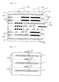
- Fig. 2 schematically shows an outline cross-sectional view of a multilayered wiring board 1 (hereinafter sometimes abbreviated as "board 1"), in which a dielectric layer 2 and a conductor layer 3 are alternately formed, and if desired, a semiconductor element 51 is mounted on the surface thereof. Respective wiring layers playing a role of wiring in the conductor layer 3 are electrically connected to each other by via holes 35 each penetrating through the wiring layer in the thickness direction. Further, in Fig. 2, there is constituted an entire electrode conductor layer 11 in which a part of the conductor layer 3 functions as an ground conductor for noise protection.
- a part of the wiring layer in the conductor layer 3 can be constituted as a strip line.
- the wiring board 1 may be a high-frequency package or one provided with an active element function having an ability for processing high-frequency signals itself, or may be one mounting a high-frequency element individually constituted, such as an antenna switch module.
- the board 1 of this embodiment is incorporated with various thick-film circuit elements such as a capacitor 54, an inductor 53, and a resistor 55, in addition to the conductor layer 3, but it may be constituted as a board having only the conductor layer 3 without particularly having the thick-film circuit elements.
- the board 1 can be applied to known wiring boards such as a mode comprising a high-frequency wiring layer 10 such as a high-frequency micro-strip line.
- the capacitor electrode in the capacitor 54 in Fig. 2 can be made the entire electrode conductor layer 11.
- the electrode layer 11 that functions as the shield portion for noise protection, functions as the ground conductor such as s trip line, or functions as the capacitor electrode is required to be large so as to have a forming area of 1 cm 2 or more.
- the dielectric layer 2 using a crystallized glass and the conductor layer 3 containing the electrode layer 11 are simultaneously sintered, there was hitherto a problem that blister or gap is liable to generate in the formed conductor layer 3, especially in the electrode layer 11, leading to reduction of the function of the electrode layer 11.
- the glass as a constitutional component of the dielectric layer 2 has a crystallization temperature exceeding 1,000 °C
- the glass is one in which the crystallization is inhibited during the sintering, or one in which no crystallization occurs at the sintering temperature of from 800 to 1,000 °C. Accordingly, it is possible to inhibit the generation of blister or gap as conventionally observed in the formed conductor layer due to the difference in the sintering shrinkage behavior between the dielectric layer and the conductor layer. As a result, it is possible to enhance the electric characteristics such as resistivity in the conductor layer, especially to form a conductor layer suitable for high-frequency signals. Further, since the electrode layer can have a forming area of 1 cm 2 or more, and the number of formed layers can be increased, not only the function of the electrode layer can be enhanced, but also a multilayered wiring board suitable for high-frequency signals can be provided.
- the glass constituting the dielectric layer of the second embodiment of the invention can be employed ones comprising SiO 2 and B 2 O 3 as major components and Al 2 O 3 and an alkaline earth metal oxide as sub-components, in which a content of the major components is from 80 to 95 mole %.
- silica, alumina, magnesia, zirconia, titania, mullite, spinel, and glass frit may be added.
- the production process of the glass in the second embodiment of the invention is not particularly limited, one example will be described below.
- Oxides of raw material elements in the raw material constituting the glass are weighed and mixed such that the material after sintering becomes one as specified previously; and the mixture is, for example, calcined at 1, 600 °C in a crucible and then pulverized by a ball mill, etc., to obtain a glass powder.
- the pulverization may be achieved such that the glass powder has a mean particle size ranging from 1 to 3 ⁇ m
- the mean particle size of the glass powder is larger than 3 ⁇ m, the mechanical strength of the formed dielectric layer is lowered, whereas when it is smaller than 1 ⁇ m, the debinding properties are lowered.
- the formed glass powder has a crystallization temperature exceeding 1,000 °C.
- a green sheet that will become a dielectric layer is prepared.
- the green sheet is prepared by compounding a glass powder having a mean particle size ranging from 1 to 3 ⁇ m, which can be formed by the foregoing step, with ceramic fillers such as alumina, mullite, aluminum nitride, and silicon nitride and additives such as a binder, a solvent, a plasticizer, a deflocculating agent, a surfactant, and a wetting agent and molding the mixture in a sheet-like state by the doctor blade process or the like.
- ceramic fillers such as alumina, mullite, aluminum nitride, and silicon nitride
- additives such as a binder, a solvent, a plasticizer, a deflocculating agent, a surfactant, and a wetting agent and molding the mixture in a sheet-like state by the doctor blade process or the like.
- binder examples include acrylic resins (such as polymethyl methacrylate and poly(t-butyl methacrylate)), cellulose acetate butyrate, polyethylene, polyvinyl alcohol, and polyvinyl butyral; and examples of the solvent include acetone, methyl ethyl ketone, diacetone, methyl isobutyl ketone, benzene, bromochloroethane, ethanol, butanol, propanol, toluene, and xylene.
- acrylic resins such as polymethyl methacrylate and poly(t-butyl methacrylate)
- solvent examples include acetone, methyl ethyl ketone, diacetone, methyl isobutyl ketone, benzene, bromochloroethane, ethanol, butanol, propanol, toluene, and xylene.
- examples of the plasticizer include butylbenzyl phthalate, dibutyl phthalate, dimethyl phthalate, di-2-ethylhexyl phthalate, adipic esters, polyethylene glycol derivatives, and tricresol phosphate;
- examples of the deflocculating agent include fatty acids (such as glycerin triolate) ;
- examples of the surfactant include benzenesulfonic acid;
- examples of the wetting agent include alkylaryl polyether alcohols, polyethylene glycol ethyl ether, ethylphenyl glycol, and polyoxyethylene esters.
- the green sheet On the thus obtained green sheet are formed a plurality of wiring patterns that will become a conductor layer containing an entire electrode conductor layer having a forming area of 1 cm 2 or more (in the case of incorporating a thick-film circuit element, its element pattern is also included) by the known screen printing process. Thereafter, another ceramic green sheet is overlaid thereon, and steps of the green sheet formation and green sheet lamination are repeated, followed by heat lamination under pressure. There is thus obtained a multilayered wiring molding having a green material mainly constituted of the glass powder and the ceramic filler and the conductor layer. Incidentally, in the case where the via hole 3 5 is formed, the green sheet is bored in the position where the via is to be formed by a drill or the like, into which a metal paste is then filled. The thus formed multilayered wiring molding is sintered at the sintering temperature of lower than the crystallization temperature of the glass powder, to obtain a multilayered wiring board that will become a multilayered wiring board.
- the multilayered wiring board according the second embodiment of the invention may have a dielectric layer containing the dielectric sintered body according to the first embodiment of the invention.
- a conductor layer is preferably provided on the surface of and/or inside the dielectric layer.
- the amount of the binder was 4 % by weight on a basis of 100 % by weight of the mixed powder.
- the amount of the solvent was 100 % by weight on a basis of 100 % by weight of the mixed powder.
- the granulated powder was subjected to uniaxial molding and then to CIP at 150 MPa. Next, the molding was sintered on a ceramic setter in air at a temperature of 950 °C for 2 hours to obtain a sintered material of glass A.
- the “composition (mole %)” column shows the content of each element of Si, B, Al, Na, K, Ca and Mg converted into oxide on a basis of 100 mole % of the total sum of these elements each converted into oxide; and the “In (SiO 2 + B 2 O 3 + Na 2 O + K 2 O) (mole %)” column shows the content of Na, K, or the sum of Na and K converted into oxide on a basis of 100 mole % of the total sum of Si, B, Na and K each converted into oxide.
- the differences in the glass composition are caused by the differences in the raw materials and conditions of melting crucibles. Further, the glass compositions were identified by the chemical analysis (ICP emission).
- the sintered materials of glasses A, B and C were measured for X-ray diffraction.
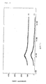
- the results of X-ray diffraction of an unsintered material and sintered material of glass B are shown in Fig. 1.
- chart (1) shows one before the sintering
- chart (2) shows one after the sintering.
- the sintered material of glass B has the same crystals as in the unsintered material.
- the sintered material of glass B is amorphous.
- glasses A and C showed similar results. Thus, it was confirmed that the sintered materials of glasses A, B and C are amorphous.
- the glass powder constituted of the glass having the composition as shown in Table 1 and a ceramic filler (particle size: 3 ⁇ m) having a composition as shown in Table 2 were mixed in a mixing ratio as shown in Table 3.
- the glass or ceramic filler marked with "*” falls outside the predetermined amount in terms of the content of the alkali metal element. Further, the ceramic filler marked with "*” falls outside the predetermined amount in terms of the content of the alkaline earth metal element.
- composition (mole %) column shows the content of each of the compounds as shown in Table 2 on a basis of 100 mole % of the total sum of these compounds; and in Table 2, the “In (SiO 2 + Al 2 O 3 Na 2 O + K 2 O) (mole %)" column shows the content of Na 2 O , K 2 O, or the sum of Na 2 O and K 2 O on a basis of 100 mole % of the total sum of SiO 2 , Al 2 O 3 , Na 2 O and K 2 O.
- the differences in the composition of the ceramic filler are caused by the differences in the raw materials and conditions of melting crucibles. Further, the compositions of the ceramic fillers were identified by the chemical analysis (ICP emission).
- the mixed powder was mixed with a binder (acrylic resin binder) and a solvent (acetone), and the mixture was then granulated to obtain a granulated powder of dielectric material.
- the amount of the binder was 4 % by weight on a basis of 100 % by weight of the mixed powder.
- the amount of the solvent was 100 % by weight on a basis of 100 % by weight of the mixed powder.
- the granulated powder was subjected to uniaxial molding and then to CIP at 150 MPa. Next, the molding was sintered on a ceramic setter in air at a temperature of 950 °C for 2 hours to obtain a dielectric sintered body.
- the dielectric sintered body was processed into a size having a diameter of from 15 to 16 mm and a thickness of from 7.5 to 8 mm. Thereafter, the dielectric sintered body was measured for specific dielectric constant and dielectric loss at TE011 mode and at a resonance frequency of from 8 to 12 GHz according to JIS R 1627. The results are shown in Table 3. Evaluation results Glass Filler Glass : Filler (Vol.
- Example 1-1 A Alumina B 64:36 5.7 0.0010 Example 1-2 B Alumina B 64:36 5.7 0.0012 Example 1-3 C * Alumina B 64:36 5.7 0.0016 Example 1-4 B Alumina A 64:36 5.7 0.0010 Example 1-5 B Alumina C * 64:36 5.7 0.0017 Example 1-6 B Alumina D ** 64:36 5.7 0.0016 Example 1-7 B Quartz 64:36 4.1 0.0014 Example 1-8 B Wallastonite ** 60:40 6.1 0.0052
- the glass having the content of the alkali metal element converted into oxide of 0.5 mole % or less when the total sum of SiO 2 , Al 2 O 3 , Na 2 O, and K 2 O in the ceramic filler is 100 mole %, in the case of using the ceramic filler containing alumina as the major component and having the content of the alkali metal element converted into oxide exceeding 0.5 mole % (Example 1-5), the specific dielectric constant showed an excellent value as 5.7, but the dielectric loss showed a large value as 0.0017.
- dielectric sintered bodys using a glass having the content of the alkali metal element exceeding 0.5 mole %, or a ceramic filler having the content of the alkali metal element exceeding 0.5 mole % are inferior in the dielectric characteristics in high-frequency regions.
- the content of the alkali metal element converted into oxide, which is contained in the glass is 0.5 mole % or less
- the content of the alkali metal element converted into oxide, which is contained in the ceramic filler is 0.5 mole % or less
- the content of the alkaline earth metal converted into oxide, which is contained in the ceramic filler is 1 mole % or less (Examples 1-4 to 6)
- the specific dielectric constant is 5.7 or less
- the dielectric loss is 0.0014 or less. Accordingly, it can be understood that these dielectric sintered bodys are superior in the dielectric characteristics in high-frequency regions.
- the dielectric sintered bodys of this Example are superior in the dielectric characteristics in high-frequency regions.
- the glass powder (particle size: 2.5 ⁇ m) of glass B as shown in Table 1 and the ceramic filler of alumina B as shown in Table 2 were mixed in a mixing ratio as shown in Table 4 to obtain a mixed powder.
- the "% by volume" as referred to herein means a rate in the true volume.
- the true volume is one calculated by dividing the weight of each powder by the particle density.
- the particle density of each of the glass powder and the ceramic filler is measured by the pycnometer method as described in JIS R 1620 "Testing Method for Particle Density of Fine Ceramic Powder".
- the mixed powder was mixed with a binder (acrylic resin binder), a plasticizer (dibutyl phthalate), and a solvent (toluene and methyl ethyl ketone) to obtain a dielectric material in a slurry state.
- a binder acrylic resin binder
- a plasticizer dibutyl phthalate
- a solvent toluene and methyl ethyl ketone
- the amount of the solvent when the weight of the mixed powder is 100 % by weight, the amount of toluene is 25 % by weight, and the amount of methyl ethyl ketone is 25 % by weight.
- a green sheet having a thickness of 250 ⁇ m was formed from the material in the slurry state by the doctor blade process. Thereafter, a Cu paste was screen printed on the surface of the green sheet, to form an unsintered pattern as a conductor layer.
- the obtained unsintered laminate was degreased at 850 °C in a moistened nitrogen atmosphere and then sintered at 1,000 °C for 2 hours in a nitrogen atmosphere, to obtain a wiring board.
- Warp of the obtained wiring board and the surface state of the dielectric layer were visually observed. The results are shown in Table 4. Further, the cross-section of the dielectric layer was subjected to textural observation by SEM. The results are also shown in Table 4. Evaluation results Glass : Filler (Vol. %) Warp Surface state Textural observation Example 2-1 75:25 Yes Gray and expanded Bubbled Example 2-2 69:31 No Gray Minute Example 2-3 64:36 No Good Minute Example 2-4 60:40 No Good Minute Example 2-5 54:46 No Good Porous
- Example 2-1 As shown in Table 4, in the case where the mixing amount of the glass powder exceeds 70 % by volume (Example 2-1), it was confirmed that warp generated in the wiring board, and bubbles generated on the surface and cross-section of the dielectric layer. It is considered that such was caused by the matter that the binder was not thoroughly removed because of a high content of the glass. This material is not suitable for use as a wiring board material.
- the wiring board was not sintered because the mixing amount of the ceramic filler was too high. This material is also not suitable for use as a wiring board material.
- the material having a mixing amount of the glass powder of from 55 to 70 % by volume is extremely suitable as a wiring board material.
- the dielectric materials according to the present invention and other present invention are constituted of a glass in which the glass powder is amorphous, they have a wide width of sintering conditions such as sintering temperature and pressure, in which a dielectric sintered body after sintering is small in specific dielectric constant and small in dielectric loss in high-frequency regions.
- sintering conditions such as sintering temperature and pressure
- a dielectric sintered body after sintering is small in specific dielectric constant and small in dielectric loss in high-frequency regions.
- the wiring board according to the invention is substantially free from warp and is superior in high-frequency characteristics in the dielectric layer.
- a mixed powder having a mean particle size of 2.5 ⁇ m of 50 parts by weight of a glass powder comprising SiO 2 , B 2 O 3 , Al 2 O 3 , and CaO as the alkaline earth metal oxide and 50 parts by weight of a ceramic filler comprising alumina was intimately mixed with 20 parts by weight of a binder (acrylic resin), 10 parts by weight of a plasticizer (dibutyl phthalate) , and 75 parts by weight of a solvent (a mixed liquid of toluene and isopropyl alcohol) , to prepare a slurry.
- a green sheet having a thickness of 250 ⁇ m was prepared by the doctor blade process.
- the obtained green sheet was pattern printed a Cu paste by the screen printing process to form an electrode layer of 3.6 x 2.6 cm 2 as a conductor layer. Further, steps of the green sheet formation and green sheet lamination were repeated to form three layers as the electrode layer. Thereafter, a green sheet was laminated so as to cover the electrode layer, to form a multilayered wiring molding. Subsequently, the multilayered wiring molding was degreased at 850 °C in a nitrogen atmosphere (reductive atmosphere) and sintered at 1,000 °C for 2 hours. There was thus obtained a multilayered board having the electrode layer formed therein.
- the Cu paste was prepared by intimately mixing 100 parts by weight of a copper powder (particle size: 5 ⁇ m) mainly constituting the electrode layer, 30 parts by weight of a vehicle, and 0.5 parts by weight of silica using a three-roll mill.
- a multilayered wiring board was prepared under the same conditions as in Example 3, except that CaO constituting the glass powder in Example 3 was replaced by a mixed powder of 60 parts by weight of a glass powder having MgO and ZnO added thereto and 40 parts by weight of a ceramic filler comprising alumina.
- a multilayered wiring board was prepared under the same conditions as in Example 3, except that a mixed powder of 60 parts by weight of a glass powder in which MgO was added to CaO as the component constituting the glass powder in Example 3 and 40 parts by weight of a ceramic filler comprising alumina.
- a multilayered wiring board was prepared under the same conditions as in Example 3, except that CaO constituting the glass powder in Example 3 was replaced by a mixed powder of 65 parts by weight of a glass powder having MgO added thereto and 35 parts by weight of a ceramic filler comprising alumina.
- the contents of the constitutional components of the glass powders in the Examples and Comparative Examples are shown in Table 5.
- the crystallization temperature in Table 5 is corresponding to an exothermic peak temperature of a differential thermal curve obtained by measuring a glass powder having the same components and contents as in each of the glass powders of the Examples and Comparative Examples by the known differential thermal analysis (DTA), prior to carrying out each of the Examples and Comparative Examples.
- the measurement of the differential thermal curve was carried out at a temperature elevation rate of 10 °C/min within the range of from 25 °C to 1,100 °C. Further, in the glass powder in Example 3, since the crystallization temperature exceeded 1,100 °C, no exothermic peak was observed within the temperature range of from 25 °C to 1,100 °C.
- the crystallization temperature of the glass power as referred to in the specification and claims of this application is corresponding to the exothermic peak temperature of the differential thermal curve as described above.
- Each of the multilayered wiring boards as prepared in the Examples and Comparative Examples was cut, and the electrode layer was visually observed under a 20-power magnifying glass.
- the Cu paste was screen printed on the surface of the green sheet to form an electrode layer pattern having a forming area of 6 mm 2 , and then, steps of the green sheet formation and green sheet lamination were repeated to form the multilayered wiring molding having an electrode layer pattern and a wiring pattern formed therein. Thereafter, the multilayered wiring molding was degreased at 850 °C in a nitrogen atmosphere (reductive atmosphere) and sintered at 1,000 °C for 2 hours. There was thus obtained a multilayered wiring board having a strip line and a micro-strip line corresponding to high-frequency signals.
- the multilayered wiring board obtained in Example 6 was subjected to dielectric measurement of specific dielectric constant and dielectric loss of the dielectric layer and to resistivity measurement of the conductor wiring as the conductor layer.
- the dielectric measurement was carried out at TE011 mode (according to JIS R 1627) and at a resonance frequency of from 8 to 12 GHz by the terminal-based short-circuiting dielectric resonator method.
- a volume resistivity of the conductor layer was determined from resistivity value of the conductor wiring obtained by the resistivity measurement and the length, width and height of the conductor wiring as measured. The both measurements were carried out at a measurement temperature of 25 °C.
- the dielectric measurement revealed that the specific dielectric constant was 5.8 and that the dielectric loss at 10 GHz was 0.0014.
- the resistivity measurement revealed that the volume resistivity was 2.4 x 10 -6 ⁇ cm.
- Example 6 It was confirmed from the measurement results of Example 6 that the multilayered wiring board having a strip line and a micro-strip line as formed in Example 6 was low in the specific dielectric constant and the dielectric loss in a high-frequency band of the dielectric layer and was low in the resistivity of the conductor layer and hence, was suitable for high-frequency signals.
- the high frequency as referred to in the specification and claims of this application means that the frequency is 1 GHz or more.
Landscapes
- Chemical & Material Sciences (AREA)
- Engineering & Computer Science (AREA)
- Materials Engineering (AREA)
- Organic Chemistry (AREA)
- Life Sciences & Earth Sciences (AREA)
- Chemical Kinetics & Catalysis (AREA)
- General Chemical & Material Sciences (AREA)
- Geochemistry & Mineralogy (AREA)
- Ceramic Engineering (AREA)
- Dispersion Chemistry (AREA)
- Inorganic Chemistry (AREA)
- Microelectronics & Electronic Packaging (AREA)
- Production Of Multi-Layered Print Wiring Board (AREA)
- Compositions Of Oxide Ceramics (AREA)
- Glass Compositions (AREA)
- Inorganic Insulating Materials (AREA)
Applications Claiming Priority (5)
| Application Number | Priority Date | Filing Date | Title |
|---|---|---|---|
| JP2001390735 | 2001-12-25 | ||
| JP2001390735A JP3752453B2 (ja) | 2001-12-25 | 2001-12-25 | 低温焼成多層配線基板及びその製造方法 |
| JP2002109646 | 2002-04-11 | ||
| JP2002109646A JP4047050B2 (ja) | 2002-04-11 | 2002-04-11 | 低温焼成磁器組成物及び低温焼成磁器並びにそれを用いた配線基板 |
| EP02028877A EP1323682A3 (fr) | 2001-12-25 | 2002-12-23 | Matériau diélectrique et corps fritté diélectrique, et carte à circuit |
Related Parent Applications (1)
| Application Number | Title | Priority Date | Filing Date |
|---|---|---|---|
| EP02028877A Division EP1323682A3 (fr) | 2001-12-25 | 2002-12-23 | Matériau diélectrique et corps fritté diélectrique, et carte à circuit |
Publications (3)
| Publication Number | Publication Date |
|---|---|
| EP1353542A2 true EP1353542A2 (fr) | 2003-10-15 |
| EP1353542A3 EP1353542A3 (fr) | 2007-09-26 |
| EP1353542B1 EP1353542B1 (fr) | 2018-05-16 |
Family
ID=26625228
Family Applications (2)
| Application Number | Title | Priority Date | Filing Date |
|---|---|---|---|
| EP02028877A Withdrawn EP1323682A3 (fr) | 2001-12-25 | 2002-12-23 | Matériau diélectrique et corps fritté diélectrique, et carte à circuit |
| EP03014167.5A Expired - Lifetime EP1353542B1 (fr) | 2001-12-25 | 2002-12-23 | Méthode de production de carte de circuit à couches multiples |
Family Applications Before (1)
| Application Number | Title | Priority Date | Filing Date |
|---|---|---|---|
| EP02028877A Withdrawn EP1323682A3 (fr) | 2001-12-25 | 2002-12-23 | Matériau diélectrique et corps fritté diélectrique, et carte à circuit |
Country Status (5)
| Country | Link |
|---|---|
| US (2) | US20030170436A1 (fr) |
| EP (2) | EP1323682A3 (fr) |
| KR (1) | KR100942615B1 (fr) |
| CN (1) | CN1329326C (fr) |
| TW (2) | TWI292391B (fr) |
Families Citing this family (48)
| Publication number | Priority date | Publication date | Assignee | Title |
|---|---|---|---|---|
| US8749054B2 (en) | 2010-06-24 | 2014-06-10 | L. Pierre de Rochemont | Semiconductor carrier with vertical power FET module |
| US7438829B2 (en) * | 2003-11-13 | 2008-10-21 | E.I. Du Pont De Nemours And Company | Thick film getter paste compositions for use in moisture control |
| JP4145262B2 (ja) * | 2004-03-23 | 2008-09-03 | 三洋電機株式会社 | 積層セラミック基板 |
| DE102004018184A1 (de) * | 2004-04-14 | 2005-11-10 | Mann + Hummel Gmbh | Adsorptionselement zur Adsorption von Dämpfen |
| JP4843611B2 (ja) * | 2004-10-01 | 2011-12-21 | デ,ロシェモント,エル.,ピエール | セラミックアンテナモジュール及びその製造方法 |
| ES2275408B1 (es) * | 2005-05-06 | 2008-04-16 | Guradoor, S.L. | Cable transportador de energia a alta tension. |
| US8350657B2 (en) | 2005-06-30 | 2013-01-08 | Derochemont L Pierre | Power management module and method of manufacture |
| CN101213638B (zh) | 2005-06-30 | 2011-07-06 | L·皮尔·德罗什蒙 | 电子元件及制造方法 |
| US20070013305A1 (en) * | 2005-07-18 | 2007-01-18 | Wang Carl B | Thick film getter paste compositions with pre-hydrated desiccant for use in atmosphere control |
| US8354294B2 (en) | 2006-01-24 | 2013-01-15 | De Rochemont L Pierre | Liquid chemical deposition apparatus and process and products therefrom |
| US7959598B2 (en) | 2008-08-20 | 2011-06-14 | Asante Solutions, Inc. | Infusion pump systems and methods |
| JP4984270B2 (ja) * | 2008-12-18 | 2012-07-25 | 日本特殊陶業株式会社 | センサ制御用回路ユニット及びガス検出装置。 |
| US8952858B2 (en) | 2009-06-17 | 2015-02-10 | L. Pierre de Rochemont | Frequency-selective dipole antennas |
| US8922347B1 (en) | 2009-06-17 | 2014-12-30 | L. Pierre de Rochemont | R.F. energy collection circuit for wireless devices |
| US8552708B2 (en) | 2010-06-02 | 2013-10-08 | L. Pierre de Rochemont | Monolithic DC/DC power management module with surface FET |
| US9023493B2 (en) | 2010-07-13 | 2015-05-05 | L. Pierre de Rochemont | Chemically complex ablative max-phase material and method of manufacture |
| EP2609626B1 (fr) | 2010-08-23 | 2024-04-03 | L. Pierre De Rochemont | Transistor à effet de champ de puissance ayant une grille de transistor résonante |
| CN103415925A (zh) | 2010-11-03 | 2013-11-27 | L·皮尔·德罗什蒙 | 具有单片集成的量子点器件的半导体芯片载体及其制造方法 |
| US8829435B2 (en) * | 2011-08-01 | 2014-09-09 | Thermo Finnigan Llc | Moldable ceramics for mass spectrometry applications |
| US9561324B2 (en) | 2013-07-19 | 2017-02-07 | Bigfoot Biomedical, Inc. | Infusion pump system and method |
| JP6691315B2 (ja) * | 2014-04-03 | 2020-04-28 | 日本電気硝子株式会社 | ガラス |
| WO2017123525A1 (fr) | 2016-01-13 | 2017-07-20 | Bigfoot Biomedical, Inc. | Interface utilisateur pour système de gestion du diabète |
| US10806859B2 (en) | 2016-01-14 | 2020-10-20 | Bigfoot Biomedical, Inc. | Adjusting insulin delivery rates |
| HK1256995A1 (zh) | 2016-01-14 | 2019-10-11 | Bigfoot Biomedical, Inc. | 药物输送设备、系统和方法中的阻塞解决方案 |
| JP6724481B2 (ja) * | 2016-03-30 | 2020-07-15 | 日立金属株式会社 | セラミック基板及びその製造方法 |
| US12383166B2 (en) | 2016-05-23 | 2025-08-12 | Insulet Corporation | Insulin delivery system and methods with risk-based set points |
| US10363374B2 (en) | 2016-05-26 | 2019-07-30 | Insulet Corporation | Multi-dose drug delivery device |
| US11096624B2 (en) | 2016-12-12 | 2021-08-24 | Bigfoot Biomedical, Inc. | Alarms and alerts for medication delivery devices and systems |
| EP3568860B1 (fr) | 2017-01-13 | 2025-12-10 | Insulet Corporation | Méthodes, systèmes et dispositifs d'administration d'insuline |
| US11033682B2 (en) | 2017-01-13 | 2021-06-15 | Bigfoot Biomedical, Inc. | Insulin delivery methods, systems and devices |
| US10583250B2 (en) | 2017-01-13 | 2020-03-10 | Bigfoot Biomedical, Inc. | System and method for adjusting insulin delivery |
| US10500334B2 (en) | 2017-01-13 | 2019-12-10 | Bigfoot Biomedical, Inc. | System and method for adjusting insulin delivery |
| US10881792B2 (en) | 2017-01-13 | 2021-01-05 | Bigfoot Biomedical, Inc. | System and method for adjusting insulin delivery |
| US10758675B2 (en) | 2017-01-13 | 2020-09-01 | Bigfoot Biomedical, Inc. | System and method for adjusting insulin delivery |
| JP6260731B1 (ja) * | 2017-02-15 | 2018-01-17 | Tdk株式会社 | ガラスセラミックス焼結体およびコイル電子部品 |
| USD874471S1 (en) | 2017-06-08 | 2020-02-04 | Insulet Corporation | Display screen with a graphical user interface |
| RU2701611C1 (ru) * | 2017-11-07 | 2019-09-30 | Ферро Корпорэйшн | Композиции диэлектрика с низкой к для применений при высоких частотах |
| USD928199S1 (en) | 2018-04-02 | 2021-08-17 | Bigfoot Biomedical, Inc. | Medication delivery device with icons |
| US12562251B1 (en) | 2018-05-09 | 2026-02-24 | Bigfoot Biomedical, Inc. | Computing architecture for assuring the provenance of medication therapy related parameters, and related systems, methods and devices |
| USD920343S1 (en) | 2019-01-09 | 2021-05-25 | Bigfoot Biomedical, Inc. | Display screen or portion thereof with graphical user interface associated with insulin delivery |
| JP7498891B2 (ja) * | 2019-08-08 | 2024-06-13 | 日本電気硝子株式会社 | ガラス粉末、誘電体材料、焼結体及び高周波用回路部材 |
| CN115103822A (zh) | 2020-01-28 | 2022-09-23 | Agc株式会社 | 玻璃组合物和复合粉末材料 |
| USD977502S1 (en) | 2020-06-09 | 2023-02-07 | Insulet Corporation | Display screen with graphical user interface |
| CA3201894A1 (fr) | 2020-12-18 | 2022-06-23 | Matthew Alles | Association d'un dispositif d'administration de medicament a une montre intelligente et a un systeme d'info-divertissement de vehicule |
| US12514980B2 (en) | 2021-06-30 | 2026-01-06 | Insulet Corporation | Adjustment of medicament delivery by a medicament delivery device based on menstrual cycle phase |
| US12521486B2 (en) | 2021-07-16 | 2026-01-13 | Insulet Corporation | Method for modification of insulin delivery during pregnancy in automatic insulin delivery systems |
| CN115733459A (zh) * | 2022-11-25 | 2023-03-03 | 常州承芯半导体有限公司 | 一种声表面波谐振装置及其形成方法、声表面波滤波装置 |
| EP4646726A1 (fr) | 2023-01-06 | 2025-11-12 | Insulet Corporation | Administration de bolus de repas lancée automatiquement ou manuellement avec assouplissement automatique ultérieur des contraintes de sécurité |
Citations (8)
| Publication number | Priority date | Publication date | Assignee | Title |
|---|---|---|---|---|
| JPS63168904A (ja) | 1986-12-29 | 1988-07-12 | 富士通株式会社 | 内層用銅ペ−スト組成物 |
| JPH06248097A (ja) | 1993-02-26 | 1994-09-06 | Kurabo Ind Ltd | フッ素樹脂表面の改質法 |
| JPH09175853A (ja) | 1995-12-25 | 1997-07-08 | Kyocera Corp | 低温焼成磁器組成物 |
| JPH10120436A (ja) | 1996-10-22 | 1998-05-12 | Nippon Electric Glass Co Ltd | ガラスセラミック誘電体材料 |
| JPH10320612A (ja) | 1997-05-16 | 1998-12-04 | Shinko Electric Co Ltd | 自動販売機 |
| JPH11214812A (ja) | 1998-01-29 | 1999-08-06 | Kyocera Corp | 高周波用配線基板 |
| JP2000143332A (ja) | 1998-11-11 | 2000-05-23 | Nec Corp | 低温焼成ガラスセラミックス |
| JP2002109646A (ja) | 2000-10-04 | 2002-04-12 | Yazaki Corp | 盗難防止機能付き警報装置 |
Family Cites Families (34)
| Publication number | Priority date | Publication date | Assignee | Title |
|---|---|---|---|---|
| US4045234A (en) * | 1976-08-23 | 1977-08-30 | Kaiser Aluminum & Chemical Corporation | Process for producing high density sintered alumina |
| JPS58151345A (ja) | 1982-02-26 | 1983-09-08 | Asahi Glass Co Ltd | 低誘電率ガラス組成物 |
| US4774211A (en) * | 1983-08-08 | 1988-09-27 | International Business Machines Corporation | Methods for predicting and controlling the shrinkage of ceramic oxides during sintering |
| JPS60136294A (ja) | 1983-12-23 | 1985-07-19 | 株式会社日立製作所 | セラミック多層配線回路板 |
| JPS61222957A (ja) | 1985-03-29 | 1986-10-03 | 株式会社住友金属セラミックス | 低温焼成セラミックスの製造法 |
| US4812422A (en) * | 1985-06-17 | 1989-03-14 | Matsushita Electric Industrial Co., Ltd. | Dielectric paste and method of manufacturing the paste |
| JPS6248097A (ja) | 1985-08-28 | 1987-03-02 | 日本特殊陶業株式会社 | 多層回路基板の製造法 |
| JP2500692B2 (ja) | 1989-10-25 | 1996-05-29 | 日本電気株式会社 | 低温焼結性低誘電率無機組成物 |
| JP2763664B2 (ja) * | 1990-07-25 | 1998-06-11 | 日本碍子株式会社 | 分布定数回路用配線基板 |
| US5206190A (en) * | 1990-09-04 | 1993-04-27 | Aluminum Company Of America | Dielectric composition containing cordierite and glass |
| JPH0517211A (ja) | 1991-03-07 | 1993-01-26 | Sumitomo Metal Ind Ltd | 基板材料及び回路基板 |
| TW259924B (en) | 1991-07-10 | 1995-10-11 | Ind Tech Res Inst | Low temperature multilayer ceramic substrate and dielectric material thereof |
| US5242867A (en) * | 1992-03-04 | 1993-09-07 | Industrial Technology Research Institute | Composition for making multilayer ceramic substrates and dielectric materials with low firing temperature |
| JPH05254923A (ja) * | 1992-03-10 | 1993-10-05 | Hitachi Ltd | セラミック組成物及びセラミック回路基板 |
| GB9222986D0 (en) * | 1992-11-03 | 1992-12-16 | Johnson Matthey Plc | Dielectric powder composition |
| JP3674929B2 (ja) | 1993-11-01 | 2005-07-27 | 日本電気硝子株式会社 | 低温焼成基板用組成物 |
| JP3690312B2 (ja) | 1994-08-19 | 2005-08-31 | 株式会社日立製作所 | 電子回路装置及び電子計算機用モジュール |
| EP0697725B1 (fr) * | 1994-08-19 | 2002-11-20 | Hitachi, Ltd. | Composition céramique pour substrat de circuit et méthode de fabrication |
| JPH0986955A (ja) * | 1995-09-29 | 1997-03-31 | Murata Mfg Co Ltd | 絶縁体用ガラス組成物、絶縁体ペースト、および厚膜印刷回路 |
| JP3339999B2 (ja) | 1995-09-29 | 2002-10-28 | 京セラ株式会社 | 配線基板とそれを用いた半導体素子収納用パッケージおよびその実装構造 |
| US5725808A (en) | 1996-05-23 | 1998-03-10 | David Sarnoff Research Center, Inc. | Multilayer co-fired ceramic compositions and ceramic-on-metal circuit board |
| JPH09241068A (ja) | 1996-03-11 | 1997-09-16 | Sumitomo Metal Ind Ltd | 低温焼成セラミックス基板 |
| KR100516043B1 (ko) | 1997-03-06 | 2005-09-26 | 라미나 세라믹스, 인크. | 수동 소자들이 내재된 세라믹 다층 인쇄 회로 기판 |
| JP3042441B2 (ja) * | 1997-03-12 | 2000-05-15 | 日本電気株式会社 | 低温焼成ガラスセラミックス基板とその製造方法 |
| JPH11335162A (ja) * | 1998-05-25 | 1999-12-07 | Murata Mfg Co Ltd | セラミック基板用組成物およびセラミック回路部品 |
| US6228788B1 (en) * | 1998-08-21 | 2001-05-08 | Advanced Ceramic X Corporation | High-frequency ceramic inductor formulation |
| US6348424B1 (en) * | 1998-11-11 | 2002-02-19 | Nec Corporation | Low-temperature calcined glass ceramic and a manufacturing process therefor |
| JP2000284472A (ja) * | 1999-01-27 | 2000-10-13 | Murata Mfg Co Ltd | 感光性絶縁体ペースト及び厚膜多層回路基板 |
| JP3651298B2 (ja) * | 1999-02-17 | 2005-05-25 | 株式会社村田製作所 | 感光性絶縁体ペースト及び厚膜多層回路基板 |
| US6602623B1 (en) * | 1999-10-27 | 2003-08-05 | Ngk Spark Plug Co., Ltd. | Low-temperature firing ceramic composition, process for producing same and wiring substrate prepared by using same |
| JP3680683B2 (ja) * | 2000-03-06 | 2005-08-10 | 株式会社村田製作所 | 絶縁体磁器組成物 |
| JP2002020162A (ja) | 2000-06-29 | 2002-01-23 | Kyocera Corp | ガラスセラミック焼結体およびそれを用いた配線基板 |
| KR100592603B1 (ko) * | 2002-05-20 | 2006-06-23 | 엔지케이 스파크 플러그 캄파니 리미티드 | 유전체 자기 |
| US6835682B2 (en) * | 2002-06-04 | 2004-12-28 | E. I. Du Pont De Nemours And Company | High thermal expansion glass and tape composition |
-
2002
- 2002-12-23 EP EP02028877A patent/EP1323682A3/fr not_active Withdrawn
- 2002-12-23 KR KR1020020082284A patent/KR100942615B1/ko not_active Expired - Fee Related
- 2002-12-23 US US10/325,859 patent/US20030170436A1/en not_active Abandoned
- 2002-12-23 EP EP03014167.5A patent/EP1353542B1/fr not_active Expired - Lifetime
- 2002-12-25 TW TW094110818A patent/TWI292391B/zh not_active IP Right Cessation
- 2002-12-25 CN CNB021588066A patent/CN1329326C/zh not_active Expired - Fee Related
- 2002-12-25 TW TW091137311A patent/TWI238813B/zh active
-
2005
- 2005-06-24 US US11/165,020 patent/US7309669B2/en not_active Expired - Fee Related
Patent Citations (8)
| Publication number | Priority date | Publication date | Assignee | Title |
|---|---|---|---|---|
| JPS63168904A (ja) | 1986-12-29 | 1988-07-12 | 富士通株式会社 | 内層用銅ペ−スト組成物 |
| JPH06248097A (ja) | 1993-02-26 | 1994-09-06 | Kurabo Ind Ltd | フッ素樹脂表面の改質法 |
| JPH09175853A (ja) | 1995-12-25 | 1997-07-08 | Kyocera Corp | 低温焼成磁器組成物 |
| JPH10120436A (ja) | 1996-10-22 | 1998-05-12 | Nippon Electric Glass Co Ltd | ガラスセラミック誘電体材料 |
| JPH10320612A (ja) | 1997-05-16 | 1998-12-04 | Shinko Electric Co Ltd | 自動販売機 |
| JPH11214812A (ja) | 1998-01-29 | 1999-08-06 | Kyocera Corp | 高周波用配線基板 |
| JP2000143332A (ja) | 1998-11-11 | 2000-05-23 | Nec Corp | 低温焼成ガラスセラミックス |
| JP2002109646A (ja) | 2000-10-04 | 2002-04-12 | Yazaki Corp | 盗難防止機能付き警報装置 |
Also Published As
| Publication number | Publication date |
|---|---|
| EP1323682A3 (fr) | 2004-01-21 |
| EP1353542B1 (fr) | 2018-05-16 |
| CN1329326C (zh) | 2007-08-01 |
| TW200524835A (en) | 2005-08-01 |
| CN1446768A (zh) | 2003-10-08 |
| EP1353542A3 (fr) | 2007-09-26 |
| US20060083930A1 (en) | 2006-04-20 |
| US20030170436A1 (en) | 2003-09-11 |
| TW200301232A (en) | 2003-07-01 |
| KR100942615B1 (ko) | 2010-02-17 |
| US7309669B2 (en) | 2007-12-18 |
| TWI238813B (en) | 2005-09-01 |
| TWI292391B (en) | 2008-01-11 |
| KR20030057325A (ko) | 2003-07-04 |
| EP1323682A2 (fr) | 2003-07-02 |
Similar Documents
| Publication | Publication Date | Title |
|---|---|---|
| US7309669B2 (en) | Dielectric material and dielectric sintered body, and wiring board using the same | |
| US6232251B1 (en) | Dielectric ceramics | |
| US7605101B2 (en) | Laminate, ceramic substrate and method for making the ceramic substrate | |
| US7015160B2 (en) | Glass ceramic dielectric material suitable for production of a microwave circuit component | |
| US6572955B2 (en) | Ceramics having excellent high-frequency characteristics and method of producing the same | |
| JP5057607B2 (ja) | ガラスセラミックスおよびその製造方法並びにそれを用いた配線基板 | |
| US6503645B1 (en) | Dielectric ceramic composition and ceramic electronic component | |
| JP4792167B2 (ja) | 磁器及びその製造方法、並びに高周波用配線基板 | |
| JP3793559B2 (ja) | 高周波用磁器組成物および高周波用磁器 | |
| JP3550270B2 (ja) | 低温焼成磁器組成物および低温焼成磁器の製造方法 | |
| JP4045127B2 (ja) | セラミック基板 | |
| JP3827491B2 (ja) | 高周波用磁器組成物および高周波用磁器並びに高周波用磁器の製造方法 | |
| JP3559407B2 (ja) | ガラスセラミック焼結体およびそれを用いた多層配線基板 | |
| JP4748701B2 (ja) | 低温焼成磁器組成物、およびそれを用いた配線基板 | |
| JP2005217170A (ja) | 複合積層セラミック電子部品 | |
| JP2002348172A (ja) | 高周波用配線基板 | |
| JP2003115218A (ja) | 誘電体磁器 | |
| JP3628146B2 (ja) | 低温焼成磁器組成物および低温焼成磁器 | |
| JP3752453B2 (ja) | 低温焼成多層配線基板及びその製造方法 | |
| JP3851823B2 (ja) | 金属体付配線基板 | |
| JP3986832B2 (ja) | 金属体付配線基板 | |
| JP4929534B2 (ja) | 低温焼成セラミックス基板 | |
| JP2005101095A (ja) | 磁器用組成物及び磁器、並びに磁器の製造方法 | |
| JP2003073162A (ja) | ガラスセラミックスおよびそれを用いた配線基板 | |
| JP2003137657A (ja) | ガラスセラミックスおよびその製造方法、並びに配線基板 |
Legal Events
| Date | Code | Title | Description |
|---|---|---|---|
| PUAI | Public reference made under article 153(3) epc to a published international application that has entered the european phase |
Free format text: ORIGINAL CODE: 0009012 |
|
| 17P | Request for examination filed |
Effective date: 20030624 |
|
| AC | Divisional application: reference to earlier application |
Ref document number: 1323682 Country of ref document: EP Kind code of ref document: P |
|
| AK | Designated contracting states |
Kind code of ref document: A2 Designated state(s): AT BE BG CH CY CZ DE DK EE ES FI FR GB GR IE IT LI LU MC NL PT SE SI SK TR |
|
| AX | Request for extension of the european patent |
Extension state: AL LT LV MK RO |
|
| PUAL | Search report despatched |
Free format text: ORIGINAL CODE: 0009013 |
|
| AK | Designated contracting states |
Kind code of ref document: A3 Designated state(s): AT BE BG CH CY CZ DE DK EE ES FI FR GB GR IE IT LI LU MC NL PT SE SI SK TR |
|
| AX | Request for extension of the european patent |
Extension state: AL LT LV MK RO |
|
| AKX | Designation fees paid |
Designated state(s): DE FR |
|
| 17Q | First examination report despatched |
Effective date: 20161115 |
|
| GRAP | Despatch of communication of intention to grant a patent |
Free format text: ORIGINAL CODE: EPIDOSNIGR1 |
|
| INTG | Intention to grant announced |
Effective date: 20170921 |
|
| GRAJ | Information related to disapproval of communication of intention to grant by the applicant or resumption of examination proceedings by the epo deleted |
Free format text: ORIGINAL CODE: EPIDOSDIGR1 |
|
| GRAP | Despatch of communication of intention to grant a patent |
Free format text: ORIGINAL CODE: EPIDOSNIGR1 |
|
| INTC | Intention to grant announced (deleted) | ||
| INTG | Intention to grant announced |
Effective date: 20180222 |
|
| GRAS | Grant fee paid |
Free format text: ORIGINAL CODE: EPIDOSNIGR3 |
|
| GRAA | (expected) grant |
Free format text: ORIGINAL CODE: 0009210 |
|
| AC | Divisional application: reference to earlier application |
Ref document number: 1323682 Country of ref document: EP Kind code of ref document: P |
|
| AK | Designated contracting states |
Kind code of ref document: B1 Designated state(s): DE FR |
|
| REG | Reference to a national code |
Ref country code: DE Ref legal event code: R096 Ref document number: 60249436 Country of ref document: DE |
|
| REG | Reference to a national code |
Ref country code: FR Ref legal event code: PLFP Year of fee payment: 17 |
|
| RIC2 | Information provided on ipc code assigned after grant |
Ipc: C03C 14/00 20060101ALI20030821BHEP Ipc: C03C 8/14 20060101ALI20030821BHEP Ipc: H05K 3/46 20060101AFI20030821BHEP |
|
| REG | Reference to a national code |
Ref country code: DE Ref legal event code: R097 Ref document number: 60249436 Country of ref document: DE |
|
| PLBE | No opposition filed within time limit |
Free format text: ORIGINAL CODE: 0009261 |
|
| STAA | Information on the status of an ep patent application or granted ep patent |
Free format text: STATUS: NO OPPOSITION FILED WITHIN TIME LIMIT |
|
| 26N | No opposition filed |
Effective date: 20190219 |
|
| PGFP | Annual fee paid to national office [announced via postgrant information from national office to epo] |
Ref country code: DE Payment date: 20211102 Year of fee payment: 20 Ref country code: FR Payment date: 20211115 Year of fee payment: 20 |
|
| REG | Reference to a national code |
Ref country code: DE Ref legal event code: R071 Ref document number: 60249436 Country of ref document: DE |