EP1355346A2 - Gerät zur Hitzebehandlung von Halbleiterschichten bei niedriger Temperatur - Google Patents
Gerät zur Hitzebehandlung von Halbleiterschichten bei niedriger Temperatur Download PDFInfo
- Publication number
- EP1355346A2 EP1355346A2 EP02356092A EP02356092A EP1355346A2 EP 1355346 A2 EP1355346 A2 EP 1355346A2 EP 02356092 A EP02356092 A EP 02356092A EP 02356092 A EP02356092 A EP 02356092A EP 1355346 A2 EP1355346 A2 EP 1355346A2
- Authority
- EP
- European Patent Office
- Prior art keywords
- heat
- apparatuses
- induction
- films
- heating
- Prior art date
- Legal status (The legal status is an assumption and is not a legal conclusion. Google has not performed a legal analysis and makes no representation as to the accuracy of the status listed.)
- Granted
Links
Images







Classifications
-
- H—ELECTRICITY
- H05—ELECTRIC TECHNIQUES NOT OTHERWISE PROVIDED FOR
- H05B—ELECTRIC HEATING; ELECTRIC LIGHT SOURCES NOT OTHERWISE PROVIDED FOR; CIRCUIT ARRANGEMENTS FOR ELECTRIC LIGHT SOURCES, IN GENERAL
- H05B6/00—Heating by electric, magnetic or electromagnetic fields
- H05B6/02—Induction heating
- H05B6/10—Induction heating apparatus, other than furnaces, for specific applications
- H05B6/105—Induction heating apparatus, other than furnaces, for specific applications using a susceptor
-
- H—ELECTRICITY
- H10—SEMICONDUCTOR DEVICES; ELECTRIC SOLID-STATE DEVICES NOT OTHERWISE PROVIDED FOR
- H10P—GENERIC PROCESSES OR APPARATUS FOR THE MANUFACTURE OR TREATMENT OF DEVICES COVERED BY CLASS H10
- H10P95/00—Generic processes or apparatus for manufacture or treatments not covered by the other groups of this subclass
- H10P95/90—Thermal treatments, e.g. annealing or sintering
-
- H—ELECTRICITY
- H10—SEMICONDUCTOR DEVICES; ELECTRIC SOLID-STATE DEVICES NOT OTHERWISE PROVIDED FOR
- H10P—GENERIC PROCESSES OR APPARATUS FOR THE MANUFACTURE OR TREATMENT OF DEVICES COVERED BY CLASS H10
- H10P72/00—Handling or holding of wafers, substrates or devices during manufacture or treatment thereof
- H10P72/04—Apparatus for manufacture or treatment
- H10P72/0431—Apparatus for thermal treatment
- H10P72/0434—Apparatus for thermal treatment mainly by convection
Definitions
- the present invention relates to apparatuses for continuous and efficient heat-treatment of semiconductor films upon thermally susceptible non-conducting substrates at a minimum thermal budget. More particularly, the invention relates to apparatuses for heat-treatment of preparing polycrystalline silicon thin-film transistors (poly-Si TFTs) and PN diodes on glass substrates for various applications of liquid crystal displays (LCDs), organic light emitting diodes (OLEDs), and solar cells.
- poly-Si TFTs polycrystalline silicon thin-film transistors
- PN diodes on glass substrates for various applications of liquid crystal displays (LCDs), organic light emitting diodes (OLEDs), and solar cells.
- LCDs liquid crystal displays
- OLEDs organic light emitting diodes
- TFTs thin film transistors
- TFT-LCDs typically uses the TFTs composing amorphous Si films as an active layer (i.e., a-Si TFT LCD).
- a-Si TFT LCD amorphous silicon films
- poly-Si TFT LCD amorphous silicon films
- uses of poly-Si TFTs provide evident advantages over a-Si TFTs, since the current derivability of poly-Si TFTs are substantially higher than that of a-Si TFTs, thus, leading to a higher operation performance.
- a poly-Si film is typically obtained through deposition of an amorphous Si film by chemical vapor deposition method (CVD) and subsequent post-deposition crystallization heat-treatments.
- CVD chemical vapor deposition method
- Solid phase crystallization is a popular method for crystallizing amorphous silicon.
- the amorphous silicon is subject to heat-treatments at temperatures approaching 600 ⁇ for a period of at least several hours.
- glass substrates are processed in a furnace having a resistive heater source.
- high thermal budget of this method leads to damage and/or distortion of used glass substrates.
- the ELC method utilizes the nano-second laser pulse to melt and solidify the amorphous silicon into a crystalline form.
- this method has critical drawbacks for its use in mass production.
- the grain structure of poly-Si film through this process is extremely sensitive to the laser beam energy, so that the uniformity in grain structure and hence the device characteristics cannot be achieved.
- the beam size of the laser is relatively small. The small beam size requires multiple laser passes or shots to complete the crystallization processes for large size glass. Since it is difficult to precisely control the laser, the multiple shots introduce non-uniformities into the crystallization process. Further, the surface of ELC poly-Si films is rough, which also degrades the performance of device.
- the ELC also has the problem of hydrogen eruption when deposited amorphous Si has high hydrogen contents, which is usually the case in the plasma enhanced chemical vapor deposition (PECVD).
- PECVD plasma enhanced chemical vapor deposition
- the heat-treatment for dehydrogenation should be required at high temperature (450 ⁇ 480 ⁇ ) for long period (>2 hrs).
- the system of ELC process equipment is complicated, expensive, and hard to be maintained.
- the MIC process involves addition of various metal elements such as Ni, Pd, Au, Ag, and Cu onto amorphous Si films in order to enhance the crystallization kinetics.
- Use of this method enhances the crystallization at low temperatures below 600 ⁇ .
- This method is limited by poor crystalline quality of poly-Si and metal contamination.
- the metal contamination causes a detrimental leakage current in the operation of poly-Si TFTs.
- Another problem of this method is a formation of metal silicides during the process. The presence of metal silicides leads to an undesirable residue problem during the following etching process step.
- n type regions such as source and drain regions of TFTs
- dopants such as arsenic, phosphorus, or boron are implanted into Si films using ion implantation or plasma doping method. After doping of dopants, silicon is annealed for electrical activation (activation anneals).
- activation anneals Similarly to a heat-treatment of crystallization, annealing is normally carried out in the furnace with a resistance heater source. This process requires high temperatures near 600 ⁇ and long duration time. Therefore, a new method for reducing thermal budget is needed and presented in the prior art.
- the excimer laser anneals (ELA) and rapid thermal anneals (RTA) are presented for those purposes.
- the ELA uses the identical process mechanism with that of the ELC, that is, rapid re-melting and solidification of poly-Si with nano-second laser pulse.
- the problem which was found in the ELC for crystallization also exists here.
- the rapid thermal changes during the ELC process leads to an introduction of high thermal stress to the poly-Si films as well as the glass, and hence, the deterioration of device reliability.
- the RTA method uses higher temperature but for short duration of time.
- the substrate is subjected to temperature approaching 700 ⁇ 1000 ⁇ during the RTA, however, the annealing process occurs relatively quickly, in minutes or seconds.
- Optical heating sources such as tungsten-halogen or Xe Arc lamps are often used as the RTA heat source.
- the problem of the RTA is that the photon radiation from those optical sources has the range of wavelength in which not only the silicon film but also the glass substrate is heated. Therefore, the glass is heated and damaged during the process.
- the objectives of the present invention are to solve the problems described above for once and all.
- the present invention provides apparatuses for continuous and efficient heat-treatment of semiconductor films upon thermally susceptible non-conducting substrates at a minimum thermal budget. That is, the apparatuses for heat-treating the semiconductor films upon the thermally susceptible non-conducting substrates comprise:
- semiconductor films are silicon films being amorphous silicon films or crystalline silicon films
- thermally susceptible non-conducting substrates are glass and plastic substrates.
- the semiconductor films can be heat-treated continuously and efficiently without damaging the thermally susceptible substrates: e.g., crystallization of amorphous silicon films at the minimum thermal budget acceptable for the use of glass, enhancing kinetics of dopant activation at the minimum thermal budget acceptable for the use of glass.
- the thermally susceptible substrates e.g., crystallization of amorphous silicon films at the minimum thermal budget acceptable for the use of glass, enhancing kinetics of dopant activation at the minimum thermal budget acceptable for the use of glass.
- Said silicon films of the heat-treatment materials are deposited on the glass substrate, in the form of either amorphous state crystallizing into polycrystalline in the case of crystallization heat-treatment, or polycrystalline state implanted by dopants (n or p type) in the case of dopant activation heat-treatment.
- Said induction coils generate alternating magnetic flux on the semiconductor films by high frequency current applied thereto, thereby heating the semiconductor films.
- one of preferable examples is that the induction coil starting at an upper end is wound in the planar form by one or more than two rounds and then turns back to that upper end to form the upper layer, and subsequently the induction coil starting at a lower end corresponding to the upper end is wound in the planar form by one or more than two rounds and then turns back to that lower end to form the lower layer.
- winding directions and round numbers of the induction coil are the same with each other. Therefore, the alternating magnetic flux can be uniformly collimated in the direction perpendicular to the semiconductor films.
- the upper end being a starting point for forming the upper layer is located in the identical direction with the lower end being a starting point for forming the lower layer. Furthermore, when the induction coil which has formed the upper layer shifts to the starting point for forming the lower layer, the portion connecting both layers becomes to protrude sideways so as to prevent the contact of the induction coil itself. Accordingly, in the view of whole configuration, the upper and lower layers are separated from each other; however, both layers are connected at the side that the induction coil starts, but they are separated at the opposite side.
- a channel through which cooling water can be circulated is formed in the induction coil (for instance, water-cooling type cupper tube).
- the number of winding layers of induction coils for forming the upper or lower layers may be more than two so at to generate further strengthened alternating magnetic flux.
- Said magnetic cores are made of laminated metal core or ferrite core. Advantages of employing magnetic core are three fold. Firstly, it enhances the strength of magnetic field substantially with low induction power. Secondly, it makes the distribution of magnetic flux more uniform. Thirdly, it makes the flux distribution to be concentrated on the region of semiconductor films, which leads to more efficient heat-treatment and to prevention of undesired interference by the magnetic flux on the conducting components installed around them (for instance, chamber wall or external heater block).
- the magnetic cores are configured to simultaneously cover the external surface and central portion of induction coil wound in the planar form to form the upper and lower layers. That is, at the cross sectional view perpendicular to the induction coil, two "E"-type magnetic cores face each other on the imaginary central plane. Therefore, the outside part of the magnetic core covers the external surface of wound induction coil and the inside part of the magnetic core is inserted in the central portion of wound induction coil. In this configuration, the strongest alternating magnetic field is generated from the inside part of the magnetic core. While the heat-treatment materials move into the space formed by the upper and lower layers, in particular, between the two inside parts of the symmetrical magnetic cores, they can be induction-heated continuously and efficiently.
- the length of gap between the upper and lower magnetic cores is not specially limited; however, if possible, it is desirable to narrow the length of gap for generation of the strong electromagnetic field.
- the gap between the two magnetic cores may be designed to become less than the wide of the magnetic cores.
- Said preheating members heat the semiconductor films to the extent that the thermally susceptible non-conducting substrates are not damaged and thus the semiconductor films can be induction-heated by the alternating magnetic flux from the induction coils.
- the induction heat used in the heat-treatment of conductive materials cannot be applied to the heat-treatment of semiconducting materials, because the latter requires the very strong induction power.
- the present inventors found that, when being heated to the specific temperature, even materials such as semiconductor films can be induction-heated with the small induction power, which is not a generally accepted idea. Accordingly, said preheating members make the semiconductor films acceptable to the condition for induction heating.
- the preheating members heat the semiconductor films prior to its movement into the space, formed by the upper and lower layers of induction coil and the magnetic cores covering them, in which the high collimated alternating magnetic field is applied.
- Such preheating members ultimately heat the semiconductor films, and the type of preheating members may be manifold as the below.
- resistance heating sources are used to uniformly heat the atmosphere around the heat-treatment materials, which can minimize damage of the substrates by heating them wholly.
- heating plates are used being made of materials with a high resistance and good heat conductivity and being an electrically non-conductive such as A1N (Aluminum Nitride) or BN (Boron Nitride), in which the heat-treatment materials put on the heating plates are heated by the conduction heat from the heating plates
- heating plates are used being made of metal or graphite with a high conductivity, in which the heating plates are heated by the induction-heating from induction coils installed above, below or side the heating plates. That is, the heating plates are heated under the alternating magnetic field through a heating mechanism of eddy currents (i.e., induction heating), and then the heat-treatment materials are heated by the conduction heat from the heating plates.
- a heating mechanism of eddy currents i.e., induction heating
- the upper limit of temperature in the preheating members should be kept lower than the distortion temperature of the thermally susceptible substrates; for example, in the case of glass, the temperature of the preheating members should be kept lower than about 600 ⁇ being the distortion temperature of glass.
- the lower limit of temperature in the preheating members is not specifically limited, since the induction-heating become possible even at the low temperature when a strong high frequency current is applied.
- the application of the strong high frequency current requires enormous energy and the cost for making induction coils providing a very high induction magnetic field becomes very high, which is not desirable. Therefore, the temperature of the preheating members according to the present invention should be kept higher than about 200 ⁇ , preferably 400 ⁇ .
- the heating temperature of the preheating members is in the range of 200 ⁇ 600 ⁇ , preferably 400 ⁇ 600 ⁇ .
- the apparatuses according to the present invention remarkably enhance the kinetics of crystallization of amorphous silicon, the solid phase crystallization (SPC) and the metal-induced crystallization (MIC).
- the apparatuses also remarkably enhance the kinetics of dopant activation of ion-implanted polycrystalline silicon.
- the possible reason for the apparatuses according to the present invention to enhance the kinetics of said heat-treatment effects may be expressed as below.
- the semiconductor films are restricted to the silicon films and the thermally susceptible non-conducting substrates are restricted to the glass substrates, respectively.
- the alternating frequency is in the range of 1 kHz ⁇ 10 MHz.
- the alternating frequency is less than 1 kHz, the electromagnetic force becomes small, whereby it is difficult to lead the crystallization.
- the alternating frequency is more than 10 MHz, it is difficult to make the induction coils and magnetic cores for generating the alternating magnetic field of large scale.
- the above range of alternating frequency may be changed more or less depending on the configuration of induction coils.
- First mechanism is a selective joule heating of silicon films.
- Amorphous or polycrystalline silicon has high resistivity values at room temperature, for instance, 10 6 ⁇ 10 10 ⁇ -cm in the case of amorphous silicon.
- silicon is intentionally heated by external heat source, joule heating of silicon though said emf does not occur.
- amorphous and polycrystalline Si are heated to elevated temperatures, their resistivities go down rapidly to the low values, for instance, 10 ⁇ 0.01 ⁇ -cm at 500 ⁇ .
- Those resistivity values are similar to those of graphite (1 ⁇ 0.001 ⁇ -cm) and thus the induction-heating becomes possible.
- the glass substrate having high resistivity values( ⁇ 10 16 ⁇ -cm) is not heated by said alternating magnetic flux.
- the glass remains to be at low temperatures pre-set by the external heating.
- Second mechanism is that said emf activates the movement of silicon atoms through a field effect functioning on the charged defects. It is known that point defects such as vacancies, interstitial atoms and impurities are electrically charged (negatively or positively) in the silicon atomic structure. Motion of those charged defects are significantly enhanced by the presence of electric field, which has been commonly reported in the academic publications (e.g., "Field-Enhanced Diffusion” in silicon, see S.M. Sze “VLSI Technology” (2 nd ed. McGraw Hill, 1988), P. 287 incorporated herein by reference).
- FIG. 1 is a schematic view of a low-temperature heat-treatment system including the low-temperature heat-treatment apparatus according to the present invention.
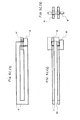
- FIGS. 2A and 2B are perspective and planar views of a second preheating chamber, an induction-heating apparatus and a first cooling chamber according to the present invention.
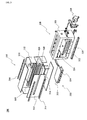
- FIG. 3 is a disassembled-perspective view of a preferred embodiment of induction-heating apparatus according to the present invention.
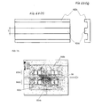
- FIGS. 4A ⁇ 4D are perspective, planar and lateral views in the assembled and disassembled forms of a preferred embodiment of an induction coil and its corresponding magnetic cores according to the present invention.
- FIGS. 5A ⁇ 5D are perspective, planar and lateral views in the assembled and disassembled forms of other preferred embodiment of an induction coil and its corresponding magnetic cores according to the present invention.
- FIGS. 6A ⁇ 6D are perspective, planar, lateral and bottom views in the assembled and disassembled forms of another preferred embodiment of an induction coil and its corresponding magnetic cores according to the present invention.
- FIGS. 7A and 7B are simulation figures regarding the distribution and strength of magnetic flux from the induction coils and magnetic cores of FIG. 6A.
- a low-temperature heat-treatment system 1000 which includes a low-temperature heat-treatment apparatus according to the present invention consists of a supply member 100, a preheating member 200, an induction heating member 300, a cooling member 400, and a manufacture member 500, which are connected in serial for the continuous process.
- Each of the preheating member 200 and cooling member 400 has two chambers (210, 220, 410, 420) for consecutive heating and cooling of heat-treatment materials.
- the sudden change of temperature may lead damage of thermally susceptible non-conducting substrates, which is not desirable.
- a second preheating chamber 220, an induction-heating member 300 and a first cooling chamber 410 are mounted in serial on a table 600 for minimizing the external effect. Also, they have closing covers 700 for the facilitation of disorder check and exchange of components during the operation.
- the induction-heating member 300 consists of a main body 310 and a fixing body 320 in which the fixing body 320 can be assembled into the main body 310.
- a fixing body 320 can be assembled and also disassembled into a main body 310 by a feed part 330.
- induction coils 810, 820 and magnetic cores 910, 920 are installed in the main body 310 in the main body 310.
- the main body 310 is covered with high frequency-shielding plates 312 made of metal such as aluminum to shield the high frequency magnetic field from the induction coils 810, 820.
- high frequency-shielding plates 312 can be assembled with jointing parts 314 and thereby also being easily disassembled.
- the induction coils 810, 820 and magnetic cores 910, 920 are supported by props 316.
- the induction coils 810, 820 are connected a power supply (not shown in the figure) of supplying the high frequency current and cooling water.
- a substrate-transfer tube 322 is connected to a box 326 through rollers 324.
- the substrate-transfer tube 322 becomes located inside the space between an upper layer induction coil 810 and a lower layer induction coil 820 in the assembled state of the main body 310 and the fixing body 320.
- the substrate-transfer tube 322 and rollers 324 which are affected by the induction magnetic field from the induction coils 810, 820 are made of materials allowing the passage of alternating magnetic field but not the generation of induction-heating, preferably quartz.
- the box 326 is not necessary to be made of the above materials such as quartz, because the alternating magnetic field from the induction coils 810, 820 is concentrated onto the substrate-transfer tube 322 by the magnetic cores 910, 920.
- a driving motor 328 installed on the lateral face of the box 326 makes heat-treatment materials (not shown in the figure) move inside the substrate-transfer tube 322.
- the box 326 is installed on the table 600 (refer to FIG. 2A) by joint parts 329.
- the main body 310 is connected to a moving part 332 and moves on a static part 334 connected to the fixing body 320.
- FIGS. 4A ⁇ 4D through FIGS. 6A ⁇ 6D shown are exemplary configurations of induction coils and magnetic cores according to preferable embodiments of the present invention.
- FIG. 4A shows in a perspective view the assembled state of configuration wherein an induction coil 800 with the square cross-section is wound as one round.
- FIG. 4B shows only the induction coil 800 in a perspective view and
- FIG. 4C(1) to 4C(3) show it in planar, front and lateral views, respectively.
- FIG. 4D(1) to 4D(2) show corresponding magnetic cores 900 in planar and lateral views.
- the induction coil 800 has a channel 810 for circulation of cooling water to prevent the induction coil 800 from being overheated.
- the induction coil 800 starting at the upper end (A) forms an upper layer 820 and lower layer 840 and then ends at the lower end (A'), wherein the upper end (A') is located at the same direction with the lower end (A).
- the induction coil 800 should not be contacted itself during the winding procedure for formation of upper layer 820 and lower layer 840.
- FIG. 4C can be referred to.
- the induction coil 800 starting at the upper end (A) is counterclockwise wound through portions 821, 822, 823, 824, 825 as one round with being kept planar to form an upper layer 840. Then, the induction coil 800 is protruded upward from portion 825 and rotated through portions 831, 832, 833, 834 on the vertical plane without being contacted itself. And, the induction coil 800 is wound in the same winding round and direction with the upper layer 820 to form a lower layer 840. Then, the induction coil 800 is protruded downward from the plane of portions 844, 845 and finally arrives at the lower end (A').
- the separate space (S) is formed between the upper layer 820 and lower layer 840, and at the direction to the upper and lower ends (A, A'), both layers are connected through the lateral portion 830 (refer to FIG. 4B), but at the opposite direction, both layers are separated.
- magnetic cores 900 corresponding to the induction coil 800 consist of an upper magnetic core 910 and lower magnetic core 920 covering each external surface of the upper layer 820 and lower layer 840.
- FIG. 4D(1) and 4D(2) show planar and lateral views of the lower magnetic core 920, wherein the outside part 922 covers the external surface of the induction coil 800 and the inside part 924 is inserted between the central portion of the induction coil 800.
- the inside part 920 provides the most strong and collimated alternating magnetic flux and hence generating the high electromagnetic force onto heat-treatment materials.
- the width (T) of the inside part 924 is designed to be larger than the width of the space (S) between the upper layer 820 and lower layer 840 of induction coil 800.
- an induction coil 800a with the rectangular cross section 810a which is designed in the same way with the winding method and round of the induction coil 800 shown in FIGS. 4A ⁇ 4D, and its corresponding magnetic cores 910a, 920a are also disclosed. Since the winding method of the induction coil 800a is the same that of the induction coil 800, the explanation thereon is omitted.
- the wide portion (x) faces the space (Sa) between the upper layer 820a and lower layer 840a at the cross-sectional view and thus the further strong alternating magnetic field is applied to the heat-treatment materials.
- FIG. 5D(1) and 5D(2) show the fact that the size of groove is larger than that in FIG. 4D because of the wide portion (x) of induction coil 800a. For this reason, the magnetic fluxes generated from the inside part of upper magnetic core 910a are introduced to the inside part 924a of lower magnetic core 920a with minimizing leakage to outside part 922a.
- FIGS. 6A ⁇ 6D an induction coil 800b with the square cross-section 810b is disclosed being wound by two rounds in the planar state.
- FIG. 6C(1) to 6C(4) show plane, front, bottom and lateral views of an induction coil 800b.
- the induction coil 800b starting at the upper end (A) is counterclockwise wound through portions 821b, 822b, 823b, 824b, 825b with being kept planar as the first round and subsequently counterclockwise wound through portions 826b, 827b, 828b, 829b inside the first round with being kept planar as the second round to form an upper layer 840b. Then, the induction coil 800b is protruded upward from portion 829 and rotated through portions 831b, 832b, 833b, 834b on the vertical plane without being contacted itself. And, the induction coil 800b is wound at the same winding direction and round with the upper layer 820b to form a lower layer 840b and finally arrives at the lower end (A').
- FIG. 6D(1) and 6D(2) disclosed is one of magnetic cores to be assembled to the induction coil 800b wound as two rounds. As can be seen from FIG. 6D(1) and 6D(2), the magnetic core is not inserted between the first round and the second round of induction coil 800b.
- FIGS. 7A and 7B shows the result of the simulation experiment using the apparatus comprising the induction coil 800b and magnetic cores 900b of FIG. 6A.
- the simulation experiment was for seeing the distribution and strength of induction magnetic fluxes.
- magnetic fluxes (arrows) generated by the induction coil 800b are concentrated between the upper layer 820b and lower layer 840b by the magnetic core.
- the magnetic fluxes are vertically applied onto the heat-treatment materials being placed in the space (Sb) between both layers 820b, 840b and thereby generating the electromagnetic force parallel to the semiconductor films.
- the magnetic fluxes generate the highest density and strongest electromagnetic force at the inside part 924b of magnetic core 920b.
- the heat-treatment materials pass through the inside part 824b by moving to the direction shown in FIG. 7A.
- the apparatuses claimed in the present invention is not limited to the specific objectives described in the present invention (i.e., crystallization of amorphous silicon and dopant activation).
- the apparatuses according to the present invention can be used in the low-temperature heat-treatment of indium-tin-oxides (ITO) or metal films on a glass (or plastic) in the display, microelectronics, and solar cell industries. It is also thought that the same means can be used in a number of other processes wherein heat-treatments of conductor or semi-conductor films upon thermally susceptible non-conducting substrates (typically glass or plastics) at a minimum thermal budget are required.
Landscapes
- Physics & Mathematics (AREA)
- Electromagnetism (AREA)
- Recrystallisation Techniques (AREA)
- Liquid Crystal (AREA)
- General Induction Heating (AREA)
Applications Claiming Priority (2)
| Application Number | Priority Date | Filing Date | Title |
|---|---|---|---|
| KR2002021503 | 2002-04-19 | ||
| KR10-2002-0021503A KR100456470B1 (ko) | 2002-04-19 | 2002-04-19 | 반도체 막의 저온 열처리 장치 |
Publications (3)
| Publication Number | Publication Date |
|---|---|
| EP1355346A2 true EP1355346A2 (de) | 2003-10-22 |
| EP1355346A3 EP1355346A3 (de) | 2004-12-15 |
| EP1355346B1 EP1355346B1 (de) | 2007-01-17 |
Family
ID=28673107
Family Applications (1)
| Application Number | Title | Priority Date | Filing Date |
|---|---|---|---|
| EP02356092A Expired - Lifetime EP1355346B1 (de) | 2002-04-19 | 2002-05-16 | Gerät zur Hitzebehandlung von Halbleiterschichten bei niedriger Temperatur |
Country Status (5)
| Country | Link |
|---|---|
| US (1) | US6747254B2 (de) |
| EP (1) | EP1355346B1 (de) |
| JP (1) | JP4074777B2 (de) |
| KR (1) | KR100456470B1 (de) |
| DE (1) | DE60217646T2 (de) |
Cited By (4)
| Publication number | Priority date | Publication date | Assignee | Title |
|---|---|---|---|---|
| FR2911130A1 (fr) * | 2007-01-05 | 2008-07-11 | Saint Gobain | Procede de depot de couche mince et produit obtenu |
| EP2103373A1 (de) * | 2008-03-20 | 2009-09-23 | komax Holding AG | Löteinrichtung zum Verbinden von Solarzellen |
| CN102481649B (zh) * | 2009-07-31 | 2014-07-23 | 科马斯控股股份公司 | 具有包括定位在与远离工件的表面的不同距离处的两个臂部的至少一个回路元件的感应焊接装置 |
| CN110181925A (zh) * | 2019-06-17 | 2019-08-30 | 徐佳辉 | 一种太阳能板交替式层压设备 |
Families Citing this family (24)
| Publication number | Priority date | Publication date | Assignee | Title |
|---|---|---|---|---|
| CA2486862C (en) * | 2002-05-30 | 2011-08-09 | Nexicor Llc | Induction seaming tapes, systems and methods |
| US6784017B2 (en) * | 2002-08-12 | 2004-08-31 | Precision Dynamics Corporation | Method of creating a high performance organic semiconductor device |
| WO2005109486A1 (en) * | 2004-05-12 | 2005-11-17 | Viatron Technologies Inc. | System for heat treatment of semiconductor device |
| KR101015595B1 (ko) * | 2005-02-28 | 2011-02-17 | 주식회사 비아트론 | 반도체 소자의 열처리 시스템 |
| JP4796056B2 (ja) * | 2004-05-12 | 2011-10-19 | ヴァイアトロン・テクノロジーズ・インコーポレーテッド | 半導体素子の熱処理システム |
| KR100580640B1 (ko) * | 2004-12-17 | 2006-05-16 | 삼성전자주식회사 | 다결정 실리콘 필름의 제조방법 및 이를 이용한 적층형트랜지스터의 제조방법 |
| CN100501550C (zh) * | 2005-11-10 | 2009-06-17 | 友达光电股份有限公司 | 具有多晶硅层的显示面板及其制造方法 |
| KR101236514B1 (ko) * | 2006-03-30 | 2013-02-21 | 엘지디스플레이 주식회사 | 반도체막 열처리 장치 |
| KR100901343B1 (ko) * | 2007-07-23 | 2009-06-05 | (주)실리콘화일 | 결정질 반도체 박막 제조 방법 |
| US7943447B2 (en) * | 2007-08-08 | 2011-05-17 | Ramesh Kakkad | Methods of fabricating crystalline silicon, thin film transistors, and solar cells |
| JP5213594B2 (ja) | 2008-09-04 | 2013-06-19 | 東京エレクトロン株式会社 | 熱処理装置 |
| TW201117672A (en) * | 2009-11-09 | 2011-05-16 | Univ Nat Formosa | Induction heating coil set |
| KR101372424B1 (ko) * | 2010-03-05 | 2014-04-18 | 주식회사 비아트론 | 결정질 실리콘 박막 형성 방법 및 이를 위한 결정질 실리콘 박막 형성 장치 |
| JPWO2012018110A1 (ja) * | 2010-08-06 | 2013-10-03 | アロニクス株式会社 | 太陽電池素子の接続装置 |
| DE102011010216A1 (de) | 2011-02-03 | 2012-08-09 | Pst Products Gmbh | Pulsschweißgerät zur Blechverschweißung |
| US8926321B2 (en) * | 2011-04-25 | 2015-01-06 | Institute of Microelectronics, Chinese Academy of Sciences | Heating method for maintaining a stable thermal budget |
| US9883551B2 (en) * | 2013-03-15 | 2018-01-30 | Silgan Containers Llc | Induction heating system for food containers and method |
| KR102206757B1 (ko) * | 2014-04-04 | 2021-01-25 | 엘지전자 주식회사 | 유도 가열 장치 및 이를 이용한 유도 가열 방법 |
| WO2015164174A1 (en) | 2014-04-24 | 2015-10-29 | Silgan Containers Llc | Food container induction heating system having power based microbial lethality monitoring |
| KR101829970B1 (ko) | 2016-02-01 | 2018-02-19 | 연세대학교 산학협력단 | 산화물 박막 트랜지스터 및 그 제조 방법 |
| KR20200015535A (ko) | 2017-05-10 | 2020-02-12 | 쉐인 토마스 맥마흔 | 박막 결정화 방법 |
| US12426132B2 (en) * | 2018-06-12 | 2025-09-23 | Carnegie Mellon University | Thermal processing techniques for metallic materials |
| US11791159B2 (en) | 2019-01-17 | 2023-10-17 | Ramesh kumar Harjivan Kakkad | Method of fabricating thin, crystalline silicon film and thin film transistors |
| US11562903B2 (en) | 2019-01-17 | 2023-01-24 | Ramesh kumar Harjivan Kakkad | Method of fabricating thin, crystalline silicon film and thin film transistors |
Family Cites Families (4)
| Publication number | Priority date | Publication date | Assignee | Title |
|---|---|---|---|---|
| DE1913676A1 (de) * | 1969-03-18 | 1970-09-24 | Siemens Ag | Verfahren zum Abscheiden von Schichten aus halbleitendem bzw. isolierendem Material aus einem stroemenden Reaktionsgas auf erhitzte Halbleiterkristalle bzw. zum Dotieren solcher Kristalle aus einem stroemenden dotierenden Gas |
| US4263336A (en) * | 1979-11-23 | 1981-04-21 | Motorola, Inc. | Reduced pressure induction heated reactor and method |
| US5578521A (en) * | 1986-11-20 | 1996-11-26 | Nippondenso Co., Ltd. | Semiconductor device with vaporphase grown epitaxial |
| JP4181761B2 (ja) * | 2001-06-21 | 2008-11-19 | ジュン キム ヒョン | 熱感受性非導電性基板上の半導体フィルムを熱処理するための方法および装置 |
-
2002
- 2002-04-19 KR KR10-2002-0021503A patent/KR100456470B1/ko not_active Expired - Fee Related
- 2002-05-14 US US10/146,504 patent/US6747254B2/en not_active Expired - Lifetime
- 2002-05-16 DE DE60217646T patent/DE60217646T2/de not_active Expired - Lifetime
- 2002-05-16 EP EP02356092A patent/EP1355346B1/de not_active Expired - Lifetime
- 2002-05-17 JP JP2002142517A patent/JP4074777B2/ja not_active Expired - Fee Related
Cited By (9)
| Publication number | Priority date | Publication date | Assignee | Title |
|---|---|---|---|---|
| FR2911130A1 (fr) * | 2007-01-05 | 2008-07-11 | Saint Gobain | Procede de depot de couche mince et produit obtenu |
| WO2008096089A3 (fr) * | 2007-01-05 | 2008-10-23 | Saint Gobain | Procede de depot de couche mince et produit obtenu |
| EA017494B1 (ru) * | 2007-01-05 | 2012-12-28 | Сэн-Гобэн Гласс Франс | Способ нанесения тонкого слоя и получаемый с использованием этого способа продукт |
| AU2008212701B2 (en) * | 2007-01-05 | 2013-07-11 | Saint-Gobain Glass France | Method for depositing a thin layer and product thus obtained |
| US9073781B2 (en) | 2007-01-05 | 2015-07-07 | Saint-Gobain Glass France | Method for depositing a thin layer and product thus obtained |
| EP2103373A1 (de) * | 2008-03-20 | 2009-09-23 | komax Holding AG | Löteinrichtung zum Verbinden von Solarzellen |
| US8680444B2 (en) | 2008-03-20 | 2014-03-25 | Komax Holding Ag | Soldering apparatus for connecting solar cells |
| CN102481649B (zh) * | 2009-07-31 | 2014-07-23 | 科马斯控股股份公司 | 具有包括定位在与远离工件的表面的不同距离处的两个臂部的至少一个回路元件的感应焊接装置 |
| CN110181925A (zh) * | 2019-06-17 | 2019-08-30 | 徐佳辉 | 一种太阳能板交替式层压设备 |
Also Published As
| Publication number | Publication date |
|---|---|
| JP2003318182A (ja) | 2003-11-07 |
| US20030197007A1 (en) | 2003-10-23 |
| KR100456470B1 (ko) | 2004-11-10 |
| EP1355346A3 (de) | 2004-12-15 |
| DE60217646T2 (de) | 2007-10-25 |
| US6747254B2 (en) | 2004-06-08 |
| EP1355346B1 (de) | 2007-01-17 |
| JP4074777B2 (ja) | 2008-04-09 |
| KR20030083099A (ko) | 2003-10-30 |
| DE60217646D1 (de) | 2007-03-08 |
Similar Documents
| Publication | Publication Date | Title |
|---|---|---|
| EP1355346B1 (de) | Gerät zur Hitzebehandlung von Halbleiterschichten bei niedriger Temperatur | |
| EP1271620B1 (de) | Verfahren und Vorrichtung zur Wärmebehandlung von Halbleiterfilmen | |
| US10840100B2 (en) | Method of thermal processing structures formed on a substrate | |
| US6334311B1 (en) | Thermoelectric-cooling temperature control apparatus for semiconductor device fabrication facility | |
| KR101826843B1 (ko) | B-필드 집중기를 사용하는 금속성 샤워헤드를 구비한 유도 플라즈마 소오스 | |
| KR102506497B1 (ko) | 인-시튜 반도체 프로세싱 챔버 온도 장치 | |
| KR20100105595A (ko) | 박막 물질들의 입자 빔 보조 변형 | |
| US8166769B2 (en) | Self-cooled vertical electronic component | |
| US20210296557A1 (en) | All-semiconductor josephson junction device for qubit applications | |
| US9601330B2 (en) | Plasma processing device, and plasma processing method | |
| CN101467236A (zh) | 避免利用焦耳加热的快速退火期间产生电弧的方法 | |
| US20050186723A1 (en) | Methods and apparatuses for heat treatment of semiconductor films upon thermally susceptible non-conducting substrates | |
| US5219798A (en) | Method of heating a semiconductor substrate capable of preventing defects in crystal from occurring | |
| KR100920399B1 (ko) | 냉각블럭 및 이를 포함하는 기판처리장치 | |
| US20060163490A1 (en) | Ion implantation cooling system | |
| US20150221475A1 (en) | Plasma processing device and plasma processing method | |
| Fiory | Rapid thermal processing for silicon nanoelectronics applications | |
| TW200533775A (en) | Method and apparatus for heat treatment of film, manufacturing method of film semiconductor element, and electro-optics device | |
| KR100387522B1 (ko) | 열안정성이 취약한 비전도성 기판상의 반도체 박막의열처리 장치 및 방법 | |
| CN112385028B (zh) | 低热量预算退火 | |
| Timans et al. | Millisecond annealing for semiconductor device applications | |
| JPH0669549A (ja) | 熱電装置 | |
| CN108461373B (zh) | 一种等离子体激活掺杂装置 | |
| Thompson et al. | Electromagnetic fast firing for ultrashallow junction formation | |
| JP6450932B2 (ja) | プラズマ処理装置及び方法 |
Legal Events
| Date | Code | Title | Description |
|---|---|---|---|
| PUAI | Public reference made under article 153(3) epc to a published international application that has entered the european phase |
Free format text: ORIGINAL CODE: 0009012 |
|
| AK | Designated contracting states |
Kind code of ref document: A2 Designated state(s): AT BE CH CY DE DK ES FI FR GB GR IE IT LI LU MC NL PT SE TR |
|
| AX | Request for extension of the european patent |
Extension state: AL LT LV MK RO SI |
|
| PUAL | Search report despatched |
Free format text: ORIGINAL CODE: 0009013 |
|
| AK | Designated contracting states |
Kind code of ref document: A3 Designated state(s): AT BE CH CY DE DK ES FI FR GB GR IE IT LI LU MC NL PT SE TR |
|
| AX | Request for extension of the european patent |
Extension state: AL LT LV MK RO SI |
|
| 17P | Request for examination filed |
Effective date: 20050428 |
|
| AKX | Designation fees paid |
Designated state(s): DE FR GB IT |
|
| GRAP | Despatch of communication of intention to grant a patent |
Free format text: ORIGINAL CODE: EPIDOSNIGR1 |
|
| GRAS | Grant fee paid |
Free format text: ORIGINAL CODE: EPIDOSNIGR3 |
|
| GRAA | (expected) grant |
Free format text: ORIGINAL CODE: 0009210 |
|
| AK | Designated contracting states |
Kind code of ref document: B1 Designated state(s): DE FR GB IT |
|
| REG | Reference to a national code |
Ref country code: GB Ref legal event code: FG4D |
|
| REF | Corresponds to: |
Ref document number: 60217646 Country of ref document: DE Date of ref document: 20070308 Kind code of ref document: P |
|
| ET | Fr: translation filed | ||
| PLBE | No opposition filed within time limit |
Free format text: ORIGINAL CODE: 0009261 |
|
| STAA | Information on the status of an ep patent application or granted ep patent |
Free format text: STATUS: NO OPPOSITION FILED WITHIN TIME LIMIT |
|
| 26N | No opposition filed |
Effective date: 20071018 |
|
| GBPC | Gb: european patent ceased through non-payment of renewal fee |
Effective date: 20070516 |
|
| PG25 | Lapsed in a contracting state [announced via postgrant information from national office to epo] |
Ref country code: IT Free format text: LAPSE BECAUSE OF FAILURE TO SUBMIT A TRANSLATION OF THE DESCRIPTION OR TO PAY THE FEE WITHIN THE PRESCRIBED TIME-LIMIT Effective date: 20070117 |
|
| PG25 | Lapsed in a contracting state [announced via postgrant information from national office to epo] |
Ref country code: GB Free format text: LAPSE BECAUSE OF NON-PAYMENT OF DUE FEES Effective date: 20070516 |
|
| REG | Reference to a national code |
Ref country code: FR Ref legal event code: PLFP Year of fee payment: 14 |
|
| PGFP | Annual fee paid to national office [announced via postgrant information from national office to epo] |
Ref country code: DE Payment date: 20150529 Year of fee payment: 14 |
|
| PGFP | Annual fee paid to national office [announced via postgrant information from national office to epo] |
Ref country code: FR Payment date: 20150529 Year of fee payment: 14 |
|
| REG | Reference to a national code |
Ref country code: DE Ref legal event code: R119 Ref document number: 60217646 Country of ref document: DE |
|
| REG | Reference to a national code |
Ref country code: FR Ref legal event code: ST Effective date: 20170131 |
|
| PG25 | Lapsed in a contracting state [announced via postgrant information from national office to epo] |
Ref country code: DE Free format text: LAPSE BECAUSE OF NON-PAYMENT OF DUE FEES Effective date: 20161201 Ref country code: FR Free format text: LAPSE BECAUSE OF NON-PAYMENT OF DUE FEES Effective date: 20160531 |