EP1357566A2 - Photovoltaische Zelle - Google Patents
Photovoltaische Zelle Download PDFInfo
- Publication number
- EP1357566A2 EP1357566A2 EP03252433A EP03252433A EP1357566A2 EP 1357566 A2 EP1357566 A2 EP 1357566A2 EP 03252433 A EP03252433 A EP 03252433A EP 03252433 A EP03252433 A EP 03252433A EP 1357566 A2 EP1357566 A2 EP 1357566A2
- Authority
- EP
- European Patent Office
- Prior art keywords
- semiconductor film
- electrode layer
- oxide
- inhibitor
- photovoltaic cell
- Prior art date
- Legal status (The legal status is an assumption and is not a legal conclusion. Google has not performed a legal analysis and makes no representation as to the accuracy of the status listed.)
- Granted
Links
Images
Classifications
-
- H—ELECTRICITY
- H01—ELECTRIC ELEMENTS
- H01G—CAPACITORS; CAPACITORS, RECTIFIERS, DETECTORS, SWITCHING DEVICES, LIGHT-SENSITIVE OR TEMPERATURE-SENSITIVE DEVICES OF THE ELECTROLYTIC TYPE
- H01G9/00—Electrolytic capacitors, rectifiers, detectors, switching devices, light-sensitive or temperature-sensitive devices; Processes of their manufacture
- H01G9/20—Light-sensitive devices
- H01G9/2027—Light-sensitive devices comprising an oxide semiconductor electrode
- H01G9/2031—Light-sensitive devices comprising an oxide semiconductor electrode comprising titanium oxide, e.g. TiO2
-
- H—ELECTRICITY
- H01—ELECTRIC ELEMENTS
- H01G—CAPACITORS; CAPACITORS, RECTIFIERS, DETECTORS, SWITCHING DEVICES, LIGHT-SENSITIVE OR TEMPERATURE-SENSITIVE DEVICES OF THE ELECTROLYTIC TYPE
- H01G9/00—Electrolytic capacitors, rectifiers, detectors, switching devices, light-sensitive or temperature-sensitive devices; Processes of their manufacture
- H01G9/20—Light-sensitive devices
- H01G9/2027—Light-sensitive devices comprising an oxide semiconductor electrode
- H01G9/2036—Light-sensitive devices comprising an oxide semiconductor electrode comprising mixed oxides, e.g. ZnO covered TiO2 particles
-
- H—ELECTRICITY
- H10—SEMICONDUCTOR DEVICES; ELECTRIC SOLID-STATE DEVICES NOT OTHERWISE PROVIDED FOR
- H10K—ORGANIC ELECTRIC SOLID-STATE DEVICES
- H10K30/00—Organic devices sensitive to infrared radiation, light, electromagnetic radiation of shorter wavelength or corpuscular radiation
- H10K30/10—Organic devices sensitive to infrared radiation, light, electromagnetic radiation of shorter wavelength or corpuscular radiation comprising heterojunctions between organic semiconductors and inorganic semiconductors
- H10K30/15—Sensitised wide-bandgap semiconductor devices, e.g. dye-sensitised TiO2
- H10K30/151—Sensitised wide-bandgap semiconductor devices, e.g. dye-sensitised TiO2 the wide bandgap semiconductor comprising titanium oxide, e.g. TiO2
-
- H—ELECTRICITY
- H10—SEMICONDUCTOR DEVICES; ELECTRIC SOLID-STATE DEVICES NOT OTHERWISE PROVIDED FOR
- H10K—ORGANIC ELECTRIC SOLID-STATE DEVICES
- H10K85/00—Organic materials used in the body or electrodes of devices covered by this subclass
- H10K85/30—Coordination compounds
- H10K85/341—Transition metal complexes, e.g. Ru(II)polypyridine complexes
- H10K85/344—Transition metal complexes, e.g. Ru(II)polypyridine complexes comprising ruthenium
-
- Y—GENERAL TAGGING OF NEW TECHNOLOGICAL DEVELOPMENTS; GENERAL TAGGING OF CROSS-SECTIONAL TECHNOLOGIES SPANNING OVER SEVERAL SECTIONS OF THE IPC; TECHNICAL SUBJECTS COVERED BY FORMER USPC CROSS-REFERENCE ART COLLECTIONS [XRACs] AND DIGESTS
- Y02—TECHNOLOGIES OR APPLICATIONS FOR MITIGATION OR ADAPTATION AGAINST CLIMATE CHANGE
- Y02E—REDUCTION OF GREENHOUSE GAS [GHG] EMISSIONS, RELATED TO ENERGY GENERATION, TRANSMISSION OR DISTRIBUTION
- Y02E10/00—Energy generation through renewable energy sources
- Y02E10/50—Photovoltaic [PV] energy
- Y02E10/542—Dye sensitized solar cells
-
- Y—GENERAL TAGGING OF NEW TECHNOLOGICAL DEVELOPMENTS; GENERAL TAGGING OF CROSS-SECTIONAL TECHNOLOGIES SPANNING OVER SEVERAL SECTIONS OF THE IPC; TECHNICAL SUBJECTS COVERED BY FORMER USPC CROSS-REFERENCE ART COLLECTIONS [XRACs] AND DIGESTS
- Y02—TECHNOLOGIES OR APPLICATIONS FOR MITIGATION OR ADAPTATION AGAINST CLIMATE CHANGE
- Y02E—REDUCTION OF GREENHOUSE GAS [GHG] EMISSIONS, RELATED TO ENERGY GENERATION, TRANSMISSION OR DISTRIBUTION
- Y02E10/00—Energy generation through renewable energy sources
- Y02E10/50—Photovoltaic [PV] energy
- Y02E10/549—Organic PV cells
Definitions
- the present invention relates to a photovoltaic cell rarely suffering recombination of electrons and/or reverse current (referred to as "back current” hereinafter) of electrons generated by excitation of a photosensitizer and having high photoelectric conversion efficiency.
- Metal oxide semiconductor materials having high band gap are used as, for example, photoelectric conversion materials, photocatalytic materials, optical sensors and storage battery materials (batteries).
- the photoelectric conversion materials are those from which optical energy can be continuously taken out as electrical energy and are those to convert optical energy into electrical energy using electrochemical reaction between electrodes.
- photoelectric conversion materials When such photoelectric conversion materials are irradiated with light, electrons are generated on one electrode side and move to the other electrode, and then the electrons migrate in the electrolyte as ions and return to the first electrode. Since this energy conversion is continuously made, it can be utilized for, for example, solar cells.
- a general solar cell comprises a substrate such as a glass plate having a transparent conductive film as an electrode and a semiconductor film for a photoelectric conversion material thereon, another substrate (e.g., glass plate) having a transparent conductive film as the other electrode, and an electrolyte enclosed between the electrodes.
- the photosensitizer adsorbed on the semiconductor When a photosensitizer adsorbed on the semiconductor is irradiated with, for example, sunlight, the photosensitizer absorbs light of visible region and is excited. The electrons generated by the excitation move to the semiconductor and to the transparent conductive glass electrode. Then, the electrons move to the other electrode through a conductor connecting the two electrodes. The electrons having moved to the other electrode reduce the oxidation-reduction system in the electrolyte.
- the photosensitizer having caused the electrons to move to the semiconductor is in a state of an oxidant, and this oxidant is reduced by the oxidation-reduction system in the electrolyte to returns to its original state. Thus, the electrons continuously flow, and the photoelectric conversion material functions as a solar cell.
- Japanese Patent Laid-Open Publication No. 220380/1989 describes a solar cell having a spectrosensitizing dye layer made of a transition metal complex such as a ruthenium complex on a surface of a metal oxide semiconductor.
- a solar cell having a spectrosensitizing dye layer made of a transition metal complex such as a ruthenium complex on a surface of a titanium oxide semiconductor layer doped with metal ion is described.
- the titanium oxide semiconductor film steps of applying a titania sol onto an electrode substrate, drying the sol and calcining the dried film are repeated to form a porous thick film, that is, a porous semiconductor film is formed to increase the amount of the Ru complex supported on the surface of the semiconductor film.
- the titania fine particles are calcined at a temperature of not lower than 400°C to improve conductivity.
- the present inventors have disclosed a process for producing titanium oxide semiconductor films for photovoltaic cells and a photovoltaic cell, which have been improved in the above points (Japanese Patent laid-Open Publication No. 339867/1999).
- the present inventors have disclosed a photovoltaic cell which uses, in order to inhibit the back current, a metal oxide semiconductor film composed of metal oxide particles having core-shell structure wherein the volume resistance value of the core is lower than that of the shell (Japanese Patent laid-Open Publication No. 155791/2001).
- the photoelectric conversion efficiency of the above photovoltaic cells has been improved to a certain extent, but there is a problem that the electromotive force is insufficient or the electromotive force and the photoelectric conversion efficiency are lowered after the cells are used for a long period of time.
- the adsorbed amount of the spectrosensitizing dye (photosensitizer) is not always large, so that back current is liable to take place, and the photoelectric conversion efficiency is not high.
- the photovoltaic cells tend to absorb ultraviolet rays, and therefore, if they are used for a long period of time, the photosensitizer is gradually decomposed. As a result, the electromotive force and the photoelectric conversion efficiency of the photovoltaic cells are gradually decreased, and the durability of the photovoltaic cells becomes insufficient.
- the present invention is intended to solve such problems as described above, and it is an object of the invention to provide a photovoltaic cell capable of inhibiting back current and decomposition of a spectrosensitizing dye caused by the ultraviolet rays, having high photoelectric conversion efficiency and capable of generating high electromotive force.
- the photovoltaic cell according to the invention is a photovoltaic cell comprising:
- the inhibitor of back current is preferably an oxide composed of one or more elements selected from Group IIIa and Group IIIb, and the content of the inhibitor of back current in the semiconductor film is preferably in the range of 0.05 to 20% by weight in terms of an oxide.
- the inhibitor of back current is preferably present on the surfaces of pores of the semiconductor film and/or the surfaces of metal oxide particles for constituting the semiconductor film.
- the component other than the inhibitor of back current in the semiconductor film is preferably composed of one or more metal oxides selected from titanium oxide, lanthanum oxide, zirconium oxide, niobium oxide, tungsten oxide, strontium oxide, zinc oxide, tin oxide and indium oxide.
- the photovoltaic cell preferably contains spherical particles having an average particle diameter of 5 to 3000 nm as the metal oxide.
- the pore volume of the semiconductor film is preferably in the range of 0.05 to 0.8 ml/g, and the average pore diameter is preferably in the range of 2 to 250 nm.
- the photovoltaic cell according to the invention is a photovoltaic cell comprising:
- the inhibitor of back current is contained in the semiconductor film as described above, so that back current can be inhibited, and decomposition of the spectrosensitizing dye caused by the ultraviolet rays can also be inhibited.
- the photovoltaic cell exhibits excellent photoelectric conversion efficiency.
- the inhibitor of back current has ultraviolet screening effect, the photosensitizer is not decomposed, and hence high electromotive force and high photoelectric conversion efficiency can be maintained even when the photovoltaic cell is used for a long period of time.
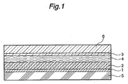
- Such a photovoltaic cell as described above is, for example, a photovoltaic cell shown in Fig. 1.
- Fig. 1 is a schematic sectional view of one embodiment of the photovoltaic cell of the present invention.
- a substrate 5 having a transparent electrode layer 1 on the surface and having a porous semiconductor film 2 which is formed on the surface of the transparent electrode layer 1 and on which a photosensitizer is adsorbed and a substrate 6 having an electrode layer 3 on the surface are arranged in such a manner that the electrode layer 1 and the electrode layer 3 face each other, and between the semiconductor film 2 and the electrode layer 3, an electrolyte 4 is held.
- a substrate that is transparent and has insulating properties for example, a glass substrate and a substrate of an organic polymer such as PET are employable.
- the substrate 6 is not particularly restricted so long as it has a strength enough to withstand the use, and for example, insulating substrates such as a glass substrate and a substrate of an organic polymer (e.g., PET) and conductive substrates such as those of metallic titanium, metallic aluminum, metallic copper and metallic nickel are employable.
- insulating substrates such as a glass substrate and a substrate of an organic polymer (e.g., PET)
- conductive substrates such as those of metallic titanium, metallic aluminum, metallic copper and metallic nickel are employable.
- any of electrodes conventionally known such as those of tin oxide, Sb-, For P-doped tin oxide, and Sn- and/or F-doped indium oxide, antimony oxide, zinc oxide and noble metal, is employable.
- the transparent electrode layer 1 can be formed by a conventional method such as thermal decomposition method or CVD method.
- the electrode layer 3 formed on the surface of the substrate 6 is not particularly restricted so long as it has catalytic reduction ability, and any of conventionally known electrodes is employable.
- Examples of such electrodes include electrodes of platinum, rhodium, metallic ruthenium and ruthenium oxide, electrodes obtained by plating or depositing these electrode materials on conductive materials such as tin oxide, Sb-, F- or P-doped tin oxide or Sn- and/or F-doped indium oxide or antimony oxide, and a carbon electrode.
- the electrode layer 3 can be directly formed on the substrate 6 by coating, plating or deposition, or can be formed by forming a conductive layer of a conductive material through a conventional method such as thermal decomposition or CVD method and then if necessary forming a layer of the above electrode material on the conductive layer through a conventional method such as plating or deposition.
- the substrate 6 may be transparent similarly to the transparent substrate 5, and the electrode layer 3 may be transparent similarly to the transparent electrode layer 1.
- the visible light transmittances of the transparent substrate 5 and the transparent electrode layer 1 are desirably high and are each preferably not less than 50%, particularly preferably not less than 90%. If the visible light transmittance is less than 50%, the photoelectric conversion efficiency is sometimes lowered.
- the resistance values of the transparent electrode layer 1 and the electrode layer 3 are each preferably not more than 100 ⁇ /cm 2 . If the resistance value of each electrode layer exceeds 100 ⁇ /cm 2 , the photoelectric conversion efficiency is sometimes lowered.
- the semiconductor film 2 may be formed on the transparent electrode layer 1 that is provided on the substrate 5, or may be formed on the electrode layer 3 that is provided on the substrate 6.
- the thickness of the semiconductor film 2 is preferably in the range of 0.1 to 50 ⁇ m.
- the semiconductor film 2 contains an inhibitor of back current.
- the inhibitor of back current used herein is an oxide composed of one or more elements selected from Group IIIa and Group IIIb.
- oxides of B, Al, Ga, In, Sc, Y, lanthanide elements and actinide elements examples include oxides of B, Al, Ga, In, Sc, Y, lanthanide elements and actinide elements, compound oxides thereof, and mixtures of two or more oxides thereof.
- oxides of B, Al and Y, compound oxides thereof and mixtures of oxides thereof are excellent in the back current inhibiting effect and ultraviolet screening effect.
- the content of the inhibitor of back current in the semiconductor film is in the range of preferably 0.05 to 20% by weight, more preferably 0.1 to 10% by weight, in terms of an oxide.
- the content (in terms of an oxide) of the inhibitor of back current in the semiconductor film is lower than the lower limit of the above range, sufficient back current inhibiting effect is not obtained, and hence the photoelectric conversion efficiency is not improved satisfactorily. Further, since the ultraviolet screening effect is not obtained, the electromotive force and the photoelectric conversion efficiency are gradually decreased, and thereby the durability sometimes becomes insufficient.
- the content (in terms of an oxide) of the inhibitor of back current in the semiconductor film exceeds the upper limit of the above range, the amount of the inhibitor of back current is so large that the layer of the inhibitor of back current becomes too thick. In some cases, moreover, pores is decreased to make diffusion of the electrolyte impossible, or the adsorbed amount of the photosensitizer becomes insufficient and thereby the photoelectric conversion efficiency becomes insufficient.
- the inhibitor of back current is preferably present on the surfaces of pores of the semiconductor film and/or the surfaces of the metal oxide particles for constituting the semiconductor film. Especially when the inhibitor of back current is so present as to cover the metal oxide particles, trapping of electrons hardly takes place on the surfaces of the pores of the semiconductor film and the surfaces of the metal oxide particles, so that the electrons move rapidly without stay on the surface area. Therefore, recombination of electrons or reverse current (back current) does not occur, and the photoelectric conversion efficiency and the electromotive force can be enhanced.
- the inhibitor of back current may be present in the form of oxide fine particles in the semiconductor film or may form a compound oxide together with the metal oxide particles for constituting the semiconductor film.
- the component other than the inhibitor of back current in the semiconductor film i.e., semiconductor component
- metal oxides selected from titanium oxide, lanthanum oxide, zirconium oxide, niobium oxide, tungsten oxide, strontium oxide, zinc oxide, tin oxide and indium oxide.
- crystalline titanium oxide such as anatase type titanium oxide, brookite type titanium oxide or rutile type titanium oxide, can be preferably employed.
- Such a metal oxide has high band gap (approx. 1.7 to 3.8 eV), so that it becomes possible that the photosensitizer absorbs visible light and is excited to generate electrons.
- Said metal oxide as the inhibitor of back current may be used as the semiconductor component.
- the oxide used as the inhibitor of back current has preferably higher bad gap than the oxide used as the semiconductor.
- the semiconductor film is desirably constituted of metal oxide spherical particles.
- the spherical particles have an average particle diameter of preferably 5 to 3000 nm, more preferably 10 to 600 nm. Also in case of the metal oxide particles coated with the inhibitor of back current, the average particle diameter is preferably in the above range.
- the average particle diameter of the metal oxide particles is less than the lower limit of the above range, cracks are liable to occur in the resulting semiconductor film, and it sometimes becomes difficult to form, by few operations, a thick film which has no cracks and has the later-described thickness. Further, the pore diameter and the pore volume of the semiconductor film are decreased, and hence the adsorbed amount of the photosensitizer is sometimes decreased. If the average particle diameter of the metal oxide particles exceeds the upper limit of the above range, large voids are produced between the particles, and hence the amount of transmitted light is increased to sometimes lower utilization of light, or the semiconductor film occasionally has insufficient strength.
- the specific surface area of the metal oxide particles is in the range of preferably 10 to 400 m 2 /g, more preferably 20 to 300 m 2 /g. If the specific surface area is less than the lower limit of the above range, the photoelectric conversion efficiency is not increased because the adsorbed amount of the photosensitizer is small. Even if the specific surface area exceeds the upper limit, there is no further increase in the photoelectric conversion efficiency.
- the pore volume of the semiconductor film is in the range of preferably 0.05 to 0.8 ml/g, more preferably 0.1 to 0.6 ml/g.
- the pore volume of the semiconductor film is less than the lower limit of the above range, the adsorbed amount of the photosensitizer is decreased. If the pore volume exceeds the upper limit, the electron mobility in the semiconductor film is lowered to sometimes decrease the photoelectric conversion efficiency.
- the semiconductor film desirably contains a binder.
- the binder is not particularly restricted, preferable is a titanium oxide binder, a zirconium oxide binder, a tungsten oxide binder or a silica binder, and particularly preferable is a titanium oxide binder.
- the titanium oxide binder is preferably one derived from peroxotitanic acid, as described later.
- the average pore diameter of the semiconductor film is in the range of preferably 2 to 250 nm, more preferably 5 to 200 nm. If the average pore diameter is less than the lower limit of the above range, the adsorbed amount of the photosensitizer is decreased. If the average pore diameter exceeds the upper limit, the electron mobility in the semiconductor film is lowered to sometimes decrease the photoelectric conversion efficiency.
- the process for producing the semiconductor film is not particularly restricted so long as the aforesaid semiconductor film can be obtained, and any of conventionally known processes is adoptable.
- the process for producing a metal oxide semiconductor film disclosed in Japanese Patent Laid-Open Publication No. 33867/1999 applied by the present applicant can be preferably employed.
- a coating solution consisting of peroxotitanic acid, metal oxide particles and a dispersion medium is applied onto an electrode formed on an insulating substrate, dried and then cured by irradiation with ultraviolet rays or by heating, to form the semiconductor film.
- peroxotitanic acid is prepared by adding hydrogen peroxide to an aqueous solution of a titanium compound or a sol or gel of hydrous titanium oxide.
- the peroxotitanic acid means hydrous titanium peroxide and has absorption in the visible region.
- the sol or gel of hydrous titanium oxide is obtained by adding an acid or an alkali to an aqueous solution of a titanium compound to hydrolyze the compound and then optionally conducting washing or washing and heat maturing.
- the titanium compound is not particularly restricted, and examples of the titanium compounds used herein include titanium salts, such as titanium halides and titanium sulfate, titanium alkoxides, such as tetraalkoxytitanium, and titanium hydride.
- an alkali preferably ammonia and/or amine
- an alkali preferably ammonia and/or amine
- the titania colloidal particles may be added as seed particles to the peroxotitanic acid and then the above steps may be repeated.
- the titania colloidal particles thus obtained are found to be those of anatase type titanium oxide, brookite type titanium oxide or rutile type titanium oxide having high crystallinity, though they vary depending upon the type and the quantity of the base used.
- the particle diameter of the anatase type titanium oxide particles is preferably in the range of 5 to 600 nm. If the particle diameter is less than 5 nm, cracks are liable to occur in the resulting semiconductor film, and it becomes difficult to form, by few operations, a thick film which has no cracks and has the later-described thickness. Further, the pore diameter and the pore volume of the semiconductor film are decreased, and thereby the adsorbed amount of the photosensitizer is decreased, so that such a particle diameter is undesirable.
- the weight ratio between the binder and the metal oxide particles is in the range of preferably 0.05 to 0.50, particularly preferably 0.1 to 0.3, in terms of TiO 2 . If the ratio is less than 0.05, absorption of light in the visible region is insufficient, and besides the effect in increase of the adsorbed amount of the photosensitizer is not obtained in some cases. If the ratio exceeds 0.50, a dense semiconductor film is not obtained and the electron mobility is not enhanced in some cases.
- the dispersion medium is not particularly restricted so long as it can disperse the binder component and the metal oxide particles and it can be removed when dried, but preferable are alcohols.
- a film-forming assistant may be contained when needed. By the addition of the film-forming assistant, viscosity of the coating solution is increased, and hence a uniformly dried film can be obtained. Further, the titania colloidal particles are densely filled, and a semiconductor film composed of titanium oxide having high adhesion to the electrode can be obtained, so that addition of the film-forming assistant is preferable.
- the film-forming assistants include polyethylene glycol, polyvinyl pyrrolidone, hydroxpropyl cellulose, polyacrylic acid and polyvinyl alcohol.
- the coating solution can be applied by a conventional method, such as dipping, spinner method, spraying, roll coating, ink jet printing or flexographic printing.
- the coating solution is applied in such an amount that the semiconductor film finally obtained should have a thickness of 0.1 to 50 ⁇ m.
- the coating solution thus applied is dried, then irradiated with ultraviolet rays to be cured, and heat treated to perform decomposition of the film-forming assistant and annealing, whereby a titanium oxide semiconductor film is formed.
- the drying temperature has only to be a temperature at which the dispersion medium can be removed.
- the irradiation dose of the ultraviolet rays though varies depending upon the content of the peroxotitanic acid, etc., has only to be that necessary for decomposing the peroxotitanic acid and curing the film.
- the thickness of the semiconductor film obtained by the above process is preferably in the range of 0.1 to 50 ⁇ m.
- the semiconductor film obtained by the conventional process as described above contains the inhibitor of back current.
- the method to introduce the inhibitor of back current into the semiconductor film is not particularly restricted.
- the semiconductor film is immersed in a solution of the inhibitor of back current (or precursor) to allow the semiconductor film to absorb the compound, optionally followed by hydrolysis to precipitate the inhibitor of back current on the semiconductor film surface. Then, the film is dried and calcined.
- a thin film layer of the inhibitor of back current may be formed by the CVD method, using a chloride, a carbonate or an alkoxide.
- the inhibitor of back current may be added after the coating solution applied onto the electrode is dried or after it is cured.
- the metal oxide particles for constituting the semiconductor film are previously coated with a layer of the inhibitor of back current and using the thus treated particles the semiconductor film is formed in the same manner as described above. More specifically, a coating solution consisting of metal oxide particles having been coated with a layer of the inhibitor of back current, peroxotitanic acid and a dispersion medium is applied onto an electrode formed on an insulating substrate, then dried and cured to form a semiconductor film.
- the metal oxide particles can be coated with a layer of the inhibitor of back current by, for example, the following method.
- the metal oxide particles titanium oxide particles
- the metal oxide particles are dispersed in a solution of the inhibitor of back current(or precursor) to allow the metal oxide particles to absorb the inhibitor of back current compound, optionally followed by hydrolysis to precipitate the compound on the surfaces of the titanium oxide particles and hydrothermal treatment in an autoclave. Then, the film is dried and calcined.
- the inhibitor of back current may be further introduced onto the surface of the semiconductor film.
- the content of the inhibitor of back current in the semiconductor film is preferably in the range of 0.05 to 20% by weight in terms of an oxide.
- the coating layer of the inhibitor of back current exerts ultraviolet screening effect, deterioration of a photosensitizer does not occur, and hence a photovoltaic cell having excellent durability can be obtained.
- a photosensitizer is adsorbed on the semiconductor film.
- the photosensitizer is not particularly restricted so long as it absorbs light of visible region and/or infrared region and is excited.
- an organic dye, a metal complex or the like is employable.
- organic dye a conventionally known organic dye having a functional group, such as carboxyl group, hdyroxyalkyl group, hydroxyl group, sulfone group or carboxyalkyl group, in its molecule is employable.
- organic dyes include metal-free phthalocyanine, cyanine dyes, metallocyanine dyes, triphenylmethane dyes, and xanthene dyes, such as Uranin, eosin, rose bengal, Rhodamine B and dibromofluorescein. These organic dyes have characteristics of a high rate of adsorption on the semiconductor film.
- metal complexes examples include metal phthalocyanines, such as copper phthalocyanine and titanyl phthalocyanine; chlorophyll; hemin; ruthenium-cis-diaquobipyridyl complexes, such as ruthenium-tris(2,2'-bispyridyl-4,4'-dicarboxylate), cis-(SCN - )-bis(2,2'-bipyridyl-4,4'-dicarboxylate)ruthenium and ruthenium-cis-diaquobis(2,2'-bipyridyl-4,4'-dicarboxylate); porphyrin complexes, such as zinc-tetra(4-carboxyphenyl)porphyrin; and complexes of ruthenium, osmium, iron and zinc, such as iron-hexacyanide complex as disclosed in Japanese Patent laid -open Publication No.220380/1989 and National Publication of
- organic dyes and metal complexes as the photosensitizers may be used singly, or may be used as a mixture of two or more organic dyes or metal complexes, or may be used in combination of the organic dye with the metal complex.
- the semiconductor film is allowed to absorb a solvent solution of the photosensitizer by dipping, spinner method or spraying and then dried.
- the absorption step may be repeated, when needed.
- the photosensitizer may be adsorbed on the semiconductor film by contacting it with the substrate (and the semiconductor film thereon) while the photosensitizer solution is refluxed under heating.
- the solvent for dissolving the photosensitizer has only to be one capable of dissolving the photosensitizer, and examples of such solvents include water, alcohols, toluene, dimethylformamide, chloroform, ethyl cellosolve, N-methylpyrrolidone and tetrahydrofuran.
- the amount of the photosensitizer adsorbed on the semiconductor film is preferably not less than 50 ⁇ g based on 1 cm 2 of the specific surface area of the semiconductor film. If the amount of the photosensitizer is less than 50 ⁇ g, the photoelectric conversion efficiency sometimes becomes insufficient.
- the semiconductor film 2 and the electrode layer 3 are arranged so as to face each other, the sides are sealed with a resin or the like, and an electrolyte is enclosed between the electrodes to form an electrolyte layer 4.
- spacer particles may be interposed between the semiconductor film and the electrode layer.
- the spacer particles may be embedded in the semiconductor film in such a manner that at least a part of the spacer particles protrude from the semiconductor film and are brought into contact with the electrode layer 3.
- the spacer particles are not particularly restricted so long as they do not injure the semiconductor film and the electrode layer and they make it possible that the semiconductor film and the electrode layer are not contacted with each other.
- spherical spacer particles, rod-like spacer particles, etc. are employable.
- insulating particles conventionally known such as particles of resins (plastics), organic-inorganic composites, metal oxides and ceramics, are employable.
- the spacer particles made of resins are, for example, resin particles disclosed in Japanese Patent Publication No. 95165/1995.
- the spacer particles made of organic-inorganic composites preferably used are, for example, particles obtained by hydrolysis of metal alkoxide, which are disclosed in Japanese Patent Laid-Open Publication No. 140472/1995 and Japanese Patent Publication No. 257392/1996.
- the spacer particles made of metal oxides or ceramics preferably used are, for example, completely spherical particles disclosed in Japanese Patent Laid-Open Publication No. 2189152/1991 and Japanese Patent Publication No. 64548/1995. Particles wherein synthetic resins are fused to the above-exemplified particles can also be preferably employed.
- particles coated with an adhesive resin can be bonded to the semiconductor film and/or the electrode layer and fixed without migration, so that they can effectively contribute to uniform gap adjustment and stress absorption.
- electrolyte a mixture of an electrochemically active salt and at least one compound to form an oxidation-reduction system is employed.
- electrochemically active salts examples include quaternary ammonium salts, such as tetrapropylammonium iodide and tetrabutylammonium iodide, imidazolium iodide, lithium iodide, 1-ethyl-3-methylimidazolium, 1-butyl-3-methylimidazolium, 1,2-dimethyl-3-propylimidazolium, 1,2-dimethylimidazolium, tetrafluoroboric acid, hexafluorophosphoric acid, trifluoromethanesulfonic acid and bistrifluoromethanesulfonic acid imide.
- the compounds to form an oxidation-reduction system include quinone, hydroquinone, iodine, potassium iodide, bromine and potassium bromide. A mixture of these compounds is also employable.
- the electrolyte may be used as it is when it is liquid, but the electrolyte is usually used as its solvent solution, namely, an electrolytic solution.
- the electrolyte concentration in the solution is preferably in the range of 0.1 to 5 mol/liter, though it varies depending upon the type of the electrolyte and the type of the solvent used.
- a solid electrolyte may be used as the electrolyte, and examples of the solid electrolytes include CuI and CuSCN.
- solvent a conventionally known solvent is employable.
- solvents include water, alcohols, oligo ethers, carbonates such as propione carbonate, phosphoric acid esters, dimethylformamide, dimethyl sulfoxide, N-methylpyrrolidone, N-vinylpyrrolidone, sulfur compounds such as sulfolane 66, ethylene carbonate, acetonitrile and ⁇ -butyrolactone.
- liquid crystals conventionally known such as smectic liquid crystal, nematic liquid crystal and cholesteric liquid crystal, can be used together with the electrolyte by adding them to the solvent, as proposed by the present applicant in Japanese Patent Laid-Open Publication No. 015182/2001.
- a non-porous metal oxide film may be interposed between the electrode layer and the photosensitizer-adsorbed semiconductor film.
- the semiconductor film contains an inhibitor of back current, so that trapping of electrons hardly takes place on the surface area of pores of the semiconductor film and on the surface area of the metal oxide particles, and therefore the electrons do not reside on the surface area and smoothly move to the electrode. Accordingly, a photovoltaic cell free from occurrence of recombination of electrons or reverse current (back current) and having high photoelectric conversion efficiency and high electromotive force can be obtained.
- the coating layer of the inhibitor of back current formed on the surface area of the pores of the semiconductor film and the surface area of the metal oxide particles exerts ultraviolet screening effect, so that deterioration of the photosensitizer does not occur, and hence a photovoltaic cell having excellent durability can be obtained.
- the average particle diameter is set forth in Table 1.
- the dispersion of titania colloidal particles (A) obtained above was concentrated to a concentration of 10%, and the resulting dispersion was mixed with the peroxotitanic acid solution prepared above.
- hydroxypropyl cellulose was added as a film-forming assistant in such an amount that titanium in the resulting mixture became 30% by weight in terms of TiO 2 , to prepare a coating solution for forming a semiconductor film.
- the coating solution was applied onto a transparent glass substrate having thereon an electrode of fluorine-doped tin oxide, subjected to air drying, then irradiated with ultraviolet rays of 6000 mJ/cm 2 by the use of a low-pressure mercury lamp to decompose the peroxo acid and to cure the film.
- the film was further heated at 300°C for 30 minutes to perform decomposition of hydroxypropyl cellulose and annealing, whereby a titanium oxide semiconductor film (A') was formed.
- the transparent glass substrate with the titanium oxide semiconductor film (A') was immersed for 1 hour, taken out of the solution, then dried and calcined at 450°C for 20 minutes to form a titanium oxide semiconductor film containing the inhibitor of back current.
- the thickness of the titanium oxide semiconductor film containing the inhibitor of back current and the pore volume and average pore diameter determined by the nitrogen adsorption method are set forth in Table 1.
- a ruthenium complex represented by cis-(SCN - )-bis(2,2'-bipyridyl-4,4'-dicarboxylate)ruthenium(II) was dissolved as a photosensitizer in ethanol to prepare a solution having a concentration of 3 ⁇ 10 -4 mol/l.
- the resulting photosensitizer solution was applied onto the titanium oxide semiconductor film by means of a 100-rpm spinner and dried. The application and drying process was repeated 5 times.
- an amount based on 1 cm 2 of the specific surface area of the titanium oxide semiconductor film is set forth in Table 1.
- the electrode prepared above was used as one electrode, and a transparent glass substrate having, as the other electrode, an electrode of fluorine-doped tin oxide and having platinum supported on the electrode was placed in such a manner that those electrodes faced each other. Then, the sides were sealed with a resin, and between the electrodes, the electrolytic solution prepared above was held. Then, the electrodes were connected by a lead wire to prepare a photovoltaic cell (A).
- the photovoltaic cell was irradiated with light having an intensity of 100 W/m 2 by means of a solar simulator at an incidence angle of 90° (90° against the cell surface) to measure Voc (voltage in a state of open circuit), Joc (density of current in case of short circuit), FF (curve factor) and ⁇ (conversion efficiency).
- Voc voltage in a state of open circuit
- Joc density of current in case of short circuit
- FF curve factor
- ⁇ conversion efficiency
- the photovoltaic cell (A) was directly irradiated with sunlight for a total period of 500 hours and then irradiated with light having an intensity of 100 W/m 2 by means of a solar simulator at an incidence angle of 90° (90° against the cell surface) to measure Voc, Joc, FF and ⁇ .
- a dispersion of titania colloidal particles (A) having a concentration of 10% by weight obtained in the same manner as in Example 1 110 g of an aluminum nitrate aqueous solution having a concentration of 1% by weight in terms of Al 2 O 3 was added, and then aqueous ammonia having a concentration of 15% by weight was added to adjust the dispersion to pH 8.5 and to hydrolyze aluminum nitrate. Subsequently, the dispersion was subjected to heat maturing at 80°C for 20 minutes, and then ammonium ion, nitric acid ion, etc.
- Example 2 a dispersion of titania colloidal particles (B) coated with Al 2 O 3 (hydrate) as an inhibitor of back current.
- the dispersion was concentrated to a concentration of 10% by weight.
- a titanium oxide semiconductor film (B) containing Al 2 O 3 as an inhibitor of back current was formed in the same manner as in Example 1, except that the dispersion (B) of titania colloidal particles (C) having a concentration of 10% by weight was used.
- Adsorption of a photosensitizer was carried out in the same manner as in Example 1.
- the amount of the photosensitizer adsorbed on the titanium oxide semiconductor film (B) is set forth in Table 1.
- a photovoltaic cell (B) was prepared in the same manner as in Example 1. Then, Voc, Joc, FF, ⁇ and durability were measured. The results are set forth in Table 1.
- a dispersion of titania colloidal particles (A) having a concentration of 10% by weight obtained in the same manner as in Example 1 200 g of a yttrium nitrate aqueous solution having a concentration of 1% by weight in terms of Y 2 O 3 was added, and then aqueous ammonia having a concentration of 15% by weight was added to adjust the dispersion to pH 7.0 and to hydrolyze yttrium nitrate. Subsequently, the dispersion was subjected to heat maturing at 80°C for 20 minutes, and then ammonium ion, nitric acid ion, etc.
- Example 2 a dispersion of titania colloidal particles (C) coated with Y 2 O 3 (hydrate) as inhibitor of back current.
- the dispersion was concentrated to a concentration of 10% by weight.
- a titanium oxide semiconductor film (C) containing Y 2 O 3 as an inhibitor of back current was formed in the same manner as in Example 1, except that the dispersion of titania colloidal particles (C) having a concentration of 10% by weight was used.
- Adsorption of a photosensitizer was carried out in the same manner as in Example 1.
- the amount of the photosensitizer adsorbed on the titanium oxide semiconductor film (C) is set forth in Table 1.
- a photovoltaic cell (C) was prepared in the same manner as in Example 1. Then, Voc, Joc, FF, ⁇ and durability were measured. The results are set forth in Table 1.
- the average particle diameter is set forth in Table 1.
- the dispersion of titania colloidal particles (D) obtained above was adjusted to a concentration of 10%.
- 550 g of an aluminum nitrate aqueous solution having a concentration of 1% by weight in terms of Al 2 O 3 was added, and then aqueous ammonia having a concentration of 15% by weight was added to adjust the dispersion to pH 8.5 and to hydrolyze aluminum nitrate.
- the dispersion was subjected to heat maturing at 80°C for 20 minutes, and then ammonium ion, nitric acid ion, etc.
- Example 2 a dispersion of titania colloidal particles (D) coated with Al 2 O 3 (hydrate) as an inhibitor of back current.
- the dispersion was concentrated to a concentration of 10% by weight.
- a titanium oxide semiconductor film (D) containing Al 2 O 3 as an inhibitor of back current was formed in the same manner as in Example 1, except that the dispersion of titania colloidal particles (D) having a concentration of 10% by weight was used.
- Adsorption of a photosensitizer was carried out in the same manner as in Example 1.
- the amount of the photosensitizer adsorbed on the titanium oxide semiconductor film (D) is set forth in Table 1.
- a photovoltaic cell (D) was prepared in the same manner as in Example 1. Then, Voc, Joc, FF, ⁇ and durability were measured. The results are set forth in Table 1.
- a dispersion of titania colloidal particles (D) having a concentration of 10% by weight obtained in the same manner as in Example 4 1000 g of a yttrium nitrate aqueous solution having a concentration of 1% by weight in terms of Y 2 O 3 was added, and then aqueous ammonia having a concentration of 15% by weight was added to adjust the dispersion to pH 7.0 and to hydrolyze yttrium nitrate. Subsequently, the dispersion was subjected to heat maturing at 80°C for 20 minutes, and then ammonium ion, nitric acid ion, etc.
- Example 2 a dispersion of titania colloidal particles (E) coated with Y 2 O 3 (hydrate) as an inhibitor of back current.
- the dispersion was concentrated to a concentration of 10% by weight.
- a titanium oxide semiconductor film (E) containing Y 2 O 3 as an inhibitor of back current was formed in the same manner as in Example 1, except that the dispersion of titania colloidal particles (E) having a concentration of 10% by weight was used.
- Adsorption of a photosensitizer was carried out in the same manner as in Example 1.
- the amount of the photosensitizer adsorbed on the titanium oxide semiconductor film (E) is set forth in Table 1.
- a photovoltaic cell (E) was prepared in the same manner as in Example 1. Then, Voc, Joc, FF, ⁇ and durability were measured. The results are set forth in Table 1.
- a titanium oxide semiconductor film (F) coated with no inhibitor of back current was formed in the same manner as in Example 1. Then, adsorption of a photosensitizer on the semiconductor film was carried out. The amount of the photosensitizer adsorbed on the titanium oxide semiconductor film (F) is set forth in Table 1. (That is to say, adsorption of an inhibitor of back current was not conducted.)
- a photovoltaic cell (F) was prepared in the same manner as in Example 1. Then, Voc, Joc, FF, ⁇ and durability were measured. The results are set forth in Table 1.
- a titanium oxide semiconductor film (G) was formed in the same manner as in Example 4, except that coating with Al 2 O 3 as the inhibitor of back current was not conducted.
- Adsorption of a photosensitizer was carried out in the same manner as in Example 1.
- the amount of the photosensitizer adsorbed on the titanium oxide semiconductor film (G) is set forth in Table 1.
- a photovoltaic cell (G) was prepared in the same manner as in Example 1. Then, Voc, Joc, FF, ⁇ and durability were measured. The results are set forth in Table 1.
Landscapes
- Engineering & Computer Science (AREA)
- Power Engineering (AREA)
- Microelectronics & Electronic Packaging (AREA)
- Chemical & Material Sciences (AREA)
- Inorganic Chemistry (AREA)
- Physics & Mathematics (AREA)
- Electromagnetism (AREA)
- Hybrid Cells (AREA)
- Photovoltaic Devices (AREA)
Applications Claiming Priority (2)
| Application Number | Priority Date | Filing Date | Title |
|---|---|---|---|
| JP2002115387A JP4392741B2 (ja) | 2002-04-17 | 2002-04-17 | 光電気セル |
| JP2002115387 | 2002-04-17 |
Publications (3)
| Publication Number | Publication Date |
|---|---|
| EP1357566A2 true EP1357566A2 (de) | 2003-10-29 |
| EP1357566A3 EP1357566A3 (de) | 2006-09-20 |
| EP1357566B1 EP1357566B1 (de) | 2010-10-06 |
Family
ID=28786724
Family Applications (1)
| Application Number | Title | Priority Date | Filing Date |
|---|---|---|---|
| EP03252433A Expired - Lifetime EP1357566B1 (de) | 2002-04-17 | 2003-04-16 | Photovoltaische Zelle |
Country Status (5)
| Country | Link |
|---|---|
| US (1) | US7420117B2 (de) |
| EP (1) | EP1357566B1 (de) |
| JP (1) | JP4392741B2 (de) |
| AU (1) | AU2003203716B2 (de) |
| DE (1) | DE60334419D1 (de) |
Cited By (5)
| Publication number | Priority date | Publication date | Assignee | Title |
|---|---|---|---|---|
| WO2006002149A1 (en) * | 2004-06-22 | 2006-01-05 | Hewlett-Packard Development Company, L.P. | Method to form a film |
| WO2007111763A3 (en) * | 2006-03-20 | 2008-02-28 | Gen Electric | Opto-electronic devices exhibiting enhanced efficiency |
| EP1717898A4 (de) * | 2004-02-13 | 2009-08-19 | Bridgestone Corp | Farbstoffsensibilisierte solarzelle |
| EP1858108A4 (de) * | 2005-01-27 | 2012-08-29 | Nippon Kayaku Kk | Modifiziertes titanoxidteilchen und dieses verwendender fotoelektrischer wandler |
| TWI426645B (zh) * | 2010-12-13 | 2014-02-11 | Innot Bioenergy Holding Co | 電池的製造方法 |
Families Citing this family (41)
| Publication number | Priority date | Publication date | Assignee | Title |
|---|---|---|---|---|
| AU753205B2 (en) * | 1998-05-29 | 2002-10-10 | Catalysts & Chemicals Industries Co., Ltd. | Method of manufacturing photoelectric cell and oxide semiconductor for photoelectric cell |
| US6900382B2 (en) | 2002-01-25 | 2005-05-31 | Konarka Technologies, Inc. | Gel electrolytes for dye sensitized solar cells |
| US7205473B2 (en) | 2002-01-25 | 2007-04-17 | Konarka Technologies, Inc. | Photovoltaic powered multimedia greeting cards and smart cards |
| US20030192585A1 (en) | 2002-01-25 | 2003-10-16 | Konarka Technologies, Inc. | Photovoltaic cells incorporating rigid substrates |
| US7351907B2 (en) | 2002-01-25 | 2008-04-01 | Konarka Technologies, Inc. | Displays with integrated photovoltaic cells |
| US6913713B2 (en) * | 2002-01-25 | 2005-07-05 | Konarka Technologies, Inc. | Photovoltaic fibers |
| US7186911B2 (en) | 2002-01-25 | 2007-03-06 | Konarka Technologies, Inc. | Methods of scoring for fabricating interconnected photovoltaic cells |
| US7414188B2 (en) | 2002-01-25 | 2008-08-19 | Konarka Technologies, Inc. | Co-sensitizers for dye sensitized solar cells |
| US6949400B2 (en) | 2002-01-25 | 2005-09-27 | Konarka Technologies, Inc. | Ultrasonic slitting of photovoltaic cells and modules |
| JP4979878B2 (ja) * | 2002-01-25 | 2012-07-18 | コナルカ テクノロジーズ インコーポレイテッド | 色素増感太陽電池の構造及び材料 |
| EP1470563A2 (de) | 2002-01-25 | 2004-10-27 | Konarka Technologies, Inc. | Photovoltaikzellekomponente und -materialien |
| WO2008139479A2 (en) * | 2007-05-15 | 2008-11-20 | 3Gsolar Ltd. | Photovoltaic cell |
| JP2004234988A (ja) * | 2003-01-30 | 2004-08-19 | Sony Corp | 光電変換素子およびその製造方法ならびに電子装置およびその製造方法ならびに半導体層およびその製造方法 |
| JP4315701B2 (ja) * | 2003-02-25 | 2009-08-19 | シャープ株式会社 | 窒化物系iii−v族化合物半導体用電極とその製造方法 |
| JP2005032852A (ja) * | 2003-07-09 | 2005-02-03 | Matsushita Electric Ind Co Ltd | 有機光電変換素子 |
| JP4579160B2 (ja) * | 2003-07-14 | 2010-11-10 | 株式会社フジクラ | 電解質組成物、これを用いた光電変換素子および色素増感太陽電池 |
| US20050014851A1 (en) * | 2003-07-18 | 2005-01-20 | Eastman Kodak Company | Colloidal core-shell assemblies and methods of preparation |
| JP4197637B2 (ja) * | 2003-09-29 | 2008-12-17 | 株式会社東芝 | 光増感型太陽電池及びその製造方法 |
| JP4635458B2 (ja) * | 2004-03-11 | 2011-02-23 | 日亜化学工業株式会社 | 半導体発光素子 |
| US20060243587A1 (en) * | 2004-05-05 | 2006-11-02 | Sustainable Technologies International Pty Ltd | Photoelectrochemical device |
| JP4635473B2 (ja) * | 2004-05-13 | 2011-02-23 | ソニー株式会社 | 光電変換素子の製造方法及び半導体電極の製造方法 |
| DE102004030628A1 (de) * | 2004-06-24 | 2006-01-19 | Konarka Technologies, Inc., Lowell | Organisches elektronisches Element mit elektrisch leitfähiger semitransparenter Schicht |
| JP4637543B2 (ja) * | 2004-10-22 | 2011-02-23 | 京セラ株式会社 | 光電変換装置およびそれを用いた光発電装置 |
| US7329877B2 (en) * | 2004-12-15 | 2008-02-12 | Honeywell International, Inc. | Photoelectrocatalytic sensor for measuring oxidizable impurities in air |
| JP4244941B2 (ja) * | 2005-02-25 | 2009-03-25 | セイコーエプソン株式会社 | 発光素子、発光装置および電子機器 |
| KR20080044233A (ko) | 2005-08-22 | 2008-05-20 | 코나르카 테크놀로지, 인코포레이티드 | 일체형 광전지를 갖는 디스플레이 |
| MX2010005814A (es) * | 2007-11-27 | 2010-10-28 | 3Gsolar Ltd | Celdas colorantes de gran área y métodos de producción de las mismas. |
| CN102265453B (zh) | 2008-10-29 | 2014-10-01 | 富士胶片株式会社 | 色素、使用其的光电转换元件、光电化学电池、及色素的制造方法 |
| US20120125781A1 (en) * | 2008-12-10 | 2012-05-24 | Zhang jin zhong | Compositions and methods for synthesis of hydrogen fuel |
| WO2010107795A1 (en) * | 2009-03-17 | 2010-09-23 | Konarka Technologies, Inc. | Metal substrate for a dye sensitized photovoltaic cell |
| KR101021567B1 (ko) * | 2009-05-25 | 2011-03-16 | 성균관대학교산학협력단 | 광촉매, 이의 제조방법 및 이를 이용한 휘발성 유기물의 분해 방법 |
| TWI399870B (zh) * | 2009-09-24 | 2013-06-21 | Univ Nat Central | Ultraviolet light photovoltaic element and manufacturing method thereof |
| JP2011070876A (ja) * | 2009-09-25 | 2011-04-07 | Fujikura Ltd | 色素増感型光電変換素子 |
| JP5620081B2 (ja) | 2009-09-28 | 2014-11-05 | 富士フイルム株式会社 | 光電変換素子の製造方法 |
| JP5524557B2 (ja) | 2009-09-28 | 2014-06-18 | 富士フイルム株式会社 | 光電変換素子の製造方法、光電変換素子、および光電気化学電池 |
| TWI450403B (zh) * | 2009-12-07 | 2014-08-21 | Ind Tech Res Inst | 染料敏化太陽電池及其製造方法 |
| KR101373503B1 (ko) | 2009-12-18 | 2014-03-14 | 엘지디스플레이 주식회사 | 염료 감응 태양전지 모듈 및 이의 제조방법 |
| US20130081686A1 (en) * | 2011-09-30 | 2013-04-04 | The University Of Chicago | Cavity mode enhancement in dye-sensitized solar cells |
| JP6159066B2 (ja) * | 2012-08-27 | 2017-07-05 | inQs株式会社 | 複合ソーラーセル |
| JP5873577B2 (ja) * | 2013-09-25 | 2016-03-01 | 積水化学工業株式会社 | 薄膜太陽電池、半導体薄膜、及び、半導体形成用塗布液 |
| WO2015160410A2 (en) * | 2014-01-24 | 2015-10-22 | The Trustees Of The University Of Pennsylvania | High-performing bulk photovoltaics |
Family Cites Families (15)
| Publication number | Priority date | Publication date | Assignee | Title |
|---|---|---|---|---|
| CH674596A5 (de) | 1988-02-12 | 1990-06-15 | Sulzer Ag | |
| ES2080313T3 (es) * | 1990-04-17 | 1996-02-01 | Ecole Polytech | Celulas fotovoltaicas. |
| US5486941A (en) | 1990-09-29 | 1996-01-23 | Sekisui Fine Chemical Co., Ltd. | Fine sphere, a spherical spacer for a liquid crystal display element and a liquid display element using the same |
| JPH0795165B2 (ja) | 1990-09-29 | 1995-10-11 | 積水ファインケミカル株式会社 | 微球体、液晶表示素子用球状スペーサー、およびそれを用いた液晶表示素子 |
| DE4207659A1 (de) | 1992-03-11 | 1993-09-16 | Abb Patent Gmbh | Verfahren zur herstellung einer photoelektrochemischen zelle sowie eine demgemaess hergestellte zelle |
| FR2694451B1 (fr) * | 1992-07-29 | 1994-09-30 | Asulab Sa | Cellule photovoltaïque. |
| JP2698541B2 (ja) | 1993-11-17 | 1998-01-19 | 株式会社日本触媒 | 液晶表示板用スペーサーおよびこれを用いた液晶表示板 |
| WO1997016838A1 (en) * | 1995-10-31 | 1997-05-09 | Ecole Polytechnique Federale De Lausanne | A battery of photovoltaic cells and process for manufacturing the same |
| JP3952103B2 (ja) | 1998-05-29 | 2007-08-01 | 触媒化成工業株式会社 | 光電気セルおよび光電気セル用金属酸化物半導体膜の製造方法 |
| AU753205B2 (en) * | 1998-05-29 | 2002-10-10 | Catalysts & Chemicals Industries Co., Ltd. | Method of manufacturing photoelectric cell and oxide semiconductor for photoelectric cell |
| US6291763B1 (en) * | 1999-04-06 | 2001-09-18 | Fuji Photo Film Co., Ltd. | Photoelectric conversion device and photo cell |
| JP2001015182A (ja) | 1999-06-30 | 2001-01-19 | Catalysts & Chem Ind Co Ltd | 光電気セル |
| JP4169138B2 (ja) | 1999-11-25 | 2008-10-22 | 日揮触媒化成株式会社 | 光電気セル |
| US6580026B1 (en) * | 1999-06-30 | 2003-06-17 | Catalysts & Chemicals Industries Co., Ltd. | Photovoltaic cell |
| EP1174891A3 (de) * | 2000-07-19 | 2004-02-25 | Fuji Photo Film Co., Ltd. | Farbstoffsensibilisierte photoelektrochemische Zelle |
-
2002
- 2002-04-17 JP JP2002115387A patent/JP4392741B2/ja not_active Expired - Lifetime
-
2003
- 2003-04-15 AU AU2003203716A patent/AU2003203716B2/en not_active Ceased
- 2003-04-16 EP EP03252433A patent/EP1357566B1/de not_active Expired - Lifetime
- 2003-04-16 DE DE60334419T patent/DE60334419D1/de not_active Expired - Lifetime
- 2003-04-17 US US10/417,659 patent/US7420117B2/en not_active Expired - Fee Related
Cited By (6)
| Publication number | Priority date | Publication date | Assignee | Title |
|---|---|---|---|---|
| EP1717898A4 (de) * | 2004-02-13 | 2009-08-19 | Bridgestone Corp | Farbstoffsensibilisierte solarzelle |
| WO2006002149A1 (en) * | 2004-06-22 | 2006-01-05 | Hewlett-Packard Development Company, L.P. | Method to form a film |
| US7575979B2 (en) | 2004-06-22 | 2009-08-18 | Hewlett-Packard Development Company, L.P. | Method to form a film |
| EP1858108A4 (de) * | 2005-01-27 | 2012-08-29 | Nippon Kayaku Kk | Modifiziertes titanoxidteilchen und dieses verwendender fotoelektrischer wandler |
| WO2007111763A3 (en) * | 2006-03-20 | 2008-02-28 | Gen Electric | Opto-electronic devices exhibiting enhanced efficiency |
| TWI426645B (zh) * | 2010-12-13 | 2014-02-11 | Innot Bioenergy Holding Co | 電池的製造方法 |
Also Published As
| Publication number | Publication date |
|---|---|
| EP1357566A3 (de) | 2006-09-20 |
| EP1357566B1 (de) | 2010-10-06 |
| AU2003203716A1 (en) | 2003-11-06 |
| JP4392741B2 (ja) | 2010-01-06 |
| AU2003203716B2 (en) | 2008-08-14 |
| US20030196692A1 (en) | 2003-10-23 |
| DE60334419D1 (de) | 2010-11-18 |
| US7420117B2 (en) | 2008-09-02 |
| JP2003308891A (ja) | 2003-10-31 |
Similar Documents
| Publication | Publication Date | Title |
|---|---|---|
| EP1357566B1 (de) | Photovoltaische Zelle | |
| EP1091440B1 (de) | Verfahren zur herstellung photoelektrischer zellen | |
| EP2151883B1 (de) | Fotoelektrische zelle und beschichtungsmittel zur bildung eines porösen halbleiterfilms für die fotoelektrische zelle | |
| US20070175510A1 (en) | Photoelectric conversion apparatus and gelling agent | |
| JP3952103B2 (ja) | 光電気セルおよび光電気セル用金属酸化物半導体膜の製造方法 | |
| WO2005112184A1 (ja) | 光電変換素子、及びこれに用いる透明導電性基板 | |
| JP2002110261A (ja) | 新規な金属酸化物粒子およびその用途 | |
| JP2001043907A (ja) | 光電気セルおよび金属酸化物半導体膜形成用塗布液、光電気セル用金属酸化物半導体膜の製造方法 | |
| JP4298195B2 (ja) | 光電気セル | |
| DE10249246B4 (de) | Farbstoffsensibilisierte photovoltaische Zelle, ein Verfahren zur Herstellung dieser photovoltaischen Zellen sowie deren Verwendung | |
| JP4215964B2 (ja) | 光電気セル | |
| JP4916683B2 (ja) | 光電気セル | |
| JP5199587B2 (ja) | 光電気セルおよびその製造方法 | |
| JP4169138B2 (ja) | 光電気セル | |
| JP5330783B2 (ja) | 光電気セル | |
| JP2006302531A (ja) | 色素増感太陽電池およびその製造方法 | |
| JP2001185245A (ja) | 光電気セルおよび該光電気セルの半導体膜形成用塗布液 | |
| JP5140031B2 (ja) | 光電気セル | |
| JP2004178885A (ja) | 光電気セル | |
| JP2001015182A (ja) | 光電気セル | |
| EP2128880A2 (de) | Beschichtungsmaterial zum Ausbilden einer porösen Metalloxid-Halbleiterschicht für ein Photoelement | |
| JP2008258099A (ja) | 光電気セルの製造方法 | |
| JP4679844B2 (ja) | 光電気セル | |
| JP2006331995A (ja) | 光電変換素子 | |
| JP4896386B2 (ja) | 光電気セル |
Legal Events
| Date | Code | Title | Description |
|---|---|---|---|
| PUAI | Public reference made under article 153(3) epc to a published international application that has entered the european phase |
Free format text: ORIGINAL CODE: 0009012 |
|
| AK | Designated contracting states |
Kind code of ref document: A2 Designated state(s): AT BE BG CH CY CZ DE DK EE ES FI FR GB GR HU IE IT LI LU MC NL PT RO SE SI SK TR |
|
| AX | Request for extension of the european patent |
Extension state: AL LT LV MK |
|
| PUAL | Search report despatched |
Free format text: ORIGINAL CODE: 0009013 |
|
| AK | Designated contracting states |
Kind code of ref document: A3 Designated state(s): AT BE BG CH CY CZ DE DK EE ES FI FR GB GR HU IE IT LI LU MC NL PT RO SE SI SK TR |
|
| AX | Request for extension of the european patent |
Extension state: AL LT LV MK |
|
| 17P | Request for examination filed |
Effective date: 20061109 |
|
| 17Q | First examination report despatched |
Effective date: 20061220 |
|
| AKX | Designation fees paid |
Designated state(s): CH DE LI NL |
|
| RAP1 | Party data changed (applicant data changed or rights of an application transferred) |
Owner name: JGC CATALYSTS AND CHEMICALS LTD. |
|
| GRAP | Despatch of communication of intention to grant a patent |
Free format text: ORIGINAL CODE: EPIDOSNIGR1 |
|
| GRAJ | Information related to disapproval of communication of intention to grant by the applicant or resumption of examination proceedings by the epo deleted |
Free format text: ORIGINAL CODE: EPIDOSDIGR1 |
|
| GRAP | Despatch of communication of intention to grant a patent |
Free format text: ORIGINAL CODE: EPIDOSNIGR1 |
|
| GRAS | Grant fee paid |
Free format text: ORIGINAL CODE: EPIDOSNIGR3 |
|
| GRAA | (expected) grant |
Free format text: ORIGINAL CODE: 0009210 |
|
| AK | Designated contracting states |
Kind code of ref document: B1 Designated state(s): CH DE LI NL |
|
| REG | Reference to a national code |
Ref country code: CH Ref legal event code: EP |
|
| REF | Corresponds to: |
Ref document number: 60334419 Country of ref document: DE Date of ref document: 20101118 Kind code of ref document: P |
|
| REG | Reference to a national code |
Ref country code: CH Ref legal event code: NV Representative=s name: BOHEST AG |
|
| REG | Reference to a national code |
Ref country code: NL Ref legal event code: VDEP Effective date: 20101006 |
|
| PG25 | Lapsed in a contracting state [announced via postgrant information from national office to epo] |
Ref country code: NL Free format text: LAPSE BECAUSE OF FAILURE TO SUBMIT A TRANSLATION OF THE DESCRIPTION OR TO PAY THE FEE WITHIN THE PRESCRIBED TIME-LIMIT Effective date: 20101006 |
|
| PLBE | No opposition filed within time limit |
Free format text: ORIGINAL CODE: 0009261 |
|
| STAA | Information on the status of an ep patent application or granted ep patent |
Free format text: STATUS: NO OPPOSITION FILED WITHIN TIME LIMIT |
|
| 26N | No opposition filed |
Effective date: 20110707 |
|
| REG | Reference to a national code |
Ref country code: DE Ref legal event code: R097 Ref document number: 60334419 Country of ref document: DE Effective date: 20110707 |
|
| REG | Reference to a national code |
Ref country code: CH Ref legal event code: PCAR Free format text: NEW ADDRESS: HOLBEINSTRASSE 36-38, 4051 BASEL (CH) |
|
| PGFP | Annual fee paid to national office [announced via postgrant information from national office to epo] |
Ref country code: DE Payment date: 20190402 Year of fee payment: 17 |
|
| PGFP | Annual fee paid to national office [announced via postgrant information from national office to epo] |
Ref country code: CH Payment date: 20190416 Year of fee payment: 17 |
|
| REG | Reference to a national code |
Ref country code: DE Ref legal event code: R119 Ref document number: 60334419 Country of ref document: DE |
|
| REG | Reference to a national code |
Ref country code: CH Ref legal event code: PL |
|
| PG25 | Lapsed in a contracting state [announced via postgrant information from national office to epo] |
Ref country code: LI Free format text: LAPSE BECAUSE OF NON-PAYMENT OF DUE FEES Effective date: 20200430 Ref country code: DE Free format text: LAPSE BECAUSE OF NON-PAYMENT OF DUE FEES Effective date: 20201103 Ref country code: CH Free format text: LAPSE BECAUSE OF NON-PAYMENT OF DUE FEES Effective date: 20200430 |