EP1359122A2 - Halbleitende Kohlenstoffnanoröhren hergestellt durch Funktionalisierung mittels Wasserstoff und Verfahren zu deren Herstellung - Google Patents
Halbleitende Kohlenstoffnanoröhren hergestellt durch Funktionalisierung mittels Wasserstoff und Verfahren zu deren Herstellung Download PDFInfo
- Publication number
- EP1359122A2 EP1359122A2 EP03252763A EP03252763A EP1359122A2 EP 1359122 A2 EP1359122 A2 EP 1359122A2 EP 03252763 A EP03252763 A EP 03252763A EP 03252763 A EP03252763 A EP 03252763A EP 1359122 A2 EP1359122 A2 EP 1359122A2
- Authority
- EP
- European Patent Office
- Prior art keywords
- carbon nanotubes
- semiconductor
- carbon
- hydrogen
- nanotubes
- Prior art date
- Legal status (The legal status is an assumption and is not a legal conclusion. Google has not performed a legal analysis and makes no representation as to the accuracy of the status listed.)
- Granted
Links
Images






Classifications
-
- B—PERFORMING OPERATIONS; TRANSPORTING
- B82—NANOTECHNOLOGY
- B82B—NANOSTRUCTURES FORMED BY MANIPULATION OF INDIVIDUAL ATOMS, MOLECULES, OR LIMITED COLLECTIONS OF ATOMS OR MOLECULES AS DISCRETE UNITS; MANUFACTURE OR TREATMENT THEREOF
- B82B1/00—Nanostructures formed by manipulation of individual atoms or molecules, or limited collections of atoms or molecules as discrete units
-
- C—CHEMISTRY; METALLURGY
- C01—INORGANIC CHEMISTRY
- C01B—NON-METALLIC ELEMENTS; COMPOUNDS THEREOF; METALLOIDS OR COMPOUNDS THEREOF NOT COVERED BY SUBCLASS C01C
- C01B32/00—Carbon; Compounds thereof
- C01B32/15—Nano-sized carbon materials
- C01B32/158—Carbon nanotubes
- C01B32/168—After-treatment
- C01B32/174—Derivatisation; Solubilisation; Dispersion in solvents
-
- B—PERFORMING OPERATIONS; TRANSPORTING
- B82—NANOTECHNOLOGY
- B82B—NANOSTRUCTURES FORMED BY MANIPULATION OF INDIVIDUAL ATOMS, MOLECULES, OR LIMITED COLLECTIONS OF ATOMS OR MOLECULES AS DISCRETE UNITS; MANUFACTURE OR TREATMENT THEREOF
- B82B3/00—Manufacture or treatment of nanostructures by manipulation of individual atoms or molecules, or limited collections of atoms or molecules as discrete units
-
- B—PERFORMING OPERATIONS; TRANSPORTING
- B82—NANOTECHNOLOGY
- B82Y—SPECIFIC USES OR APPLICATIONS OF NANOSTRUCTURES; MEASUREMENT OR ANALYSIS OF NANOSTRUCTURES; MANUFACTURE OR TREATMENT OF NANOSTRUCTURES
- B82Y10/00—Nanotechnology for information processing, storage or transmission, e.g. quantum computing or single electron logic
-
- B—PERFORMING OPERATIONS; TRANSPORTING
- B82—NANOTECHNOLOGY
- B82Y—SPECIFIC USES OR APPLICATIONS OF NANOSTRUCTURES; MEASUREMENT OR ANALYSIS OF NANOSTRUCTURES; MANUFACTURE OR TREATMENT OF NANOSTRUCTURES
- B82Y30/00—Nanotechnology for materials or surface science, e.g. nanocomposites
-
- B—PERFORMING OPERATIONS; TRANSPORTING
- B82—NANOTECHNOLOGY
- B82Y—SPECIFIC USES OR APPLICATIONS OF NANOSTRUCTURES; MEASUREMENT OR ANALYSIS OF NANOSTRUCTURES; MANUFACTURE OR TREATMENT OF NANOSTRUCTURES
- B82Y40/00—Manufacture or treatment of nanostructures
-
- C—CHEMISTRY; METALLURGY
- C01—INORGANIC CHEMISTRY
- C01B—NON-METALLIC ELEMENTS; COMPOUNDS THEREOF; METALLOIDS OR COMPOUNDS THEREOF NOT COVERED BY SUBCLASS C01C
- C01B32/00—Carbon; Compounds thereof
- C01B32/15—Nano-sized carbon materials
- C01B32/158—Carbon nanotubes
- C01B32/168—After-treatment
-
- H—ELECTRICITY
- H10—SEMICONDUCTOR DEVICES; ELECTRIC SOLID-STATE DEVICES NOT OTHERWISE PROVIDED FOR
- H10K—ORGANIC ELECTRIC SOLID-STATE DEVICES
- H10K85/00—Organic materials used in the body or electrodes of devices covered by this subclass
- H10K85/20—Carbon compounds, e.g. carbon nanotubes or fullerenes
- H10K85/221—Carbon nanotubes
-
- B—PERFORMING OPERATIONS; TRANSPORTING
- B82—NANOTECHNOLOGY
- B82Y—SPECIFIC USES OR APPLICATIONS OF NANOSTRUCTURES; MEASUREMENT OR ANALYSIS OF NANOSTRUCTURES; MANUFACTURE OR TREATMENT OF NANOSTRUCTURES
- B82Y20/00—Nanooptics, e.g. quantum optics or photonic crystals
-
- C—CHEMISTRY; METALLURGY
- C01—INORGANIC CHEMISTRY
- C01B—NON-METALLIC ELEMENTS; COMPOUNDS THEREOF; METALLOIDS OR COMPOUNDS THEREOF NOT COVERED BY SUBCLASS C01C
- C01B2202/00—Structure or properties of carbon nanotubes
- C01B2202/20—Nanotubes characterized by their properties
- C01B2202/22—Electronic properties
-
- H—ELECTRICITY
- H10—SEMICONDUCTOR DEVICES; ELECTRIC SOLID-STATE DEVICES NOT OTHERWISE PROVIDED FOR
- H10K—ORGANIC ELECTRIC SOLID-STATE DEVICES
- H10K10/00—Organic devices specially adapted for rectifying, amplifying, oscillating or switching; Organic capacitors or resistors having potential barriers
- H10K10/40—Organic transistors
- H10K10/46—Field-effect transistors, e.g. organic thin-film transistors [OTFT]
- H10K10/462—Insulated gate field-effect transistors [IGFETs]
Definitions
- the present invention relates to semiconductor carbon nanotubes functionalized by hydrogen, and more particularly, to a method for fabricating the same.
- Carbon nanotubes are tubular forms of carbon with diameters ranging from a few to tens of nanometers and lengths of tens of micrometers.
- FIG. 1 shows the configuration of a conventional carbon nanotube.
- Carbon nanotubes are formed by rolling up sheets of graphite into cylinders.
- the configuration and diameter of carbon tubes giving them unique properties are determined by the angle at which a sheet of graphite being rolled is twisted and the diameter of the carbon nanotubes at the initial stage of rolling.
- vector C h from an arbitrary start point A to an end point A', which meet when the sheet is rolled up, is shown.
- vector C h can be expressed with unit vectors ⁇ 1 and ⁇ 2 as in equation (1) below.
- C h n ⁇ 1 + m ⁇ 2
- the diameter d t of the carbon nanotube can be calculated using equation (2) below.
- d t 0.246( n 2 + nm + m 2 ) 1/2 ⁇
- Carbon nanotubes feature very high aspect ratios of 1,000 or greater and have the electrical properties of a metal or of a semiconductor depending on their diameters and configurations.
- Metallic carbon nanotubes are known to have high electrical conductance.
- SWNT single wall nanotubes
- MWNT multi-wall nanotubes
- carbon nanotubes are manufactured using arc discharging, later ablation, chemical vapor deposition (CVD), or the like.
- CVD chemical vapor deposition
- conventional techniques cannot control chirality, leading to a mixture of metallic and semiconductor carbon nanotube particles, which cannot be used to manufacture metallic nanotransistors.
- transistors manufactured from semiconductor carbon nanotubes do not work at an ambient temperature due to the small energy bandgap of the semiconductor carbon nanotubes.
- a method for converting metallic carbon nanotubes into semiconductor carbon nanotubes by separating outer walls of MWNTs to reduce the diameter of the carbon nanotubes.
- this method involves placing the metallic carbon nanotubes in contact with an electrode and applying a high current to them, so the overall process is complex.
- the method can be applied neither directly to transistors nor to SWNTs having no extra wall to be separated out.
- the present invention provides semiconductor carbon nanotubes fabricated by hydrogen functionalization.
- the present invention also provides an easy method for converting metallic carbon nanotubes into semiconductor carbon nanotubes and for converting narrow energy bandgap semiconductor carbon nanotubes into wide energy bandgap semiconductor carbon nanotubes.
- semiconductor carbon nanotubes having chemical bonds between carbon and hydrogen atoms.
- the chemical bonds between carbon and hydrogen atoms are sp 3 hybrid bonds.
- a method for fabricating semiconductor carbon nanotubes comprising: heating carbon nanotubes in a vacuum; dissociating hydrogen molecules in hydrogen gas into hydrogen atoms; and exposing the carbon nanotubes to the hydrogen gas to form chemical bonds between carbon atoms of the carbon nanotubes and the hydrogen atoms.
- heating the carbon nanotubes in a vacuum may be performed at a temperature of 100°C or greater for 2 hours or longer.
- dissociating the hydrogen molecules into the hydrogen atoms may be performed by heating at 1500°C or greater.
- the hydrogen molecules may be dissociated into the hydrogen atoms by applying an RF or DC bias voltage or using arc discharging.
- the energy bandgap of the carbon nanotubes may be controlled by varying the duration for which the carbon nanotubes are exposed to the hydrogen gas.
- the energy bandgap of the carbon nanotubes may be controlled by varying the pressure.
- the chemical bonds between the carbon and hydrogen atoms in the carbon nanotubes fabricated by the above method may be sp 3 hybrid bonds.
- metallic carbon nanotubes can be converted into semiconductor carbon nanotubes and narrow energy bandgap semiconductor carbon nanotubes can be converted into wide energy bandgap semiconductor carbon nanotubes by hydrogenation.
- the functional hydrogenated semiconductor carbon nanotubes have a wide range of applications, including use in electronic devices such as transistors, electro-optic devices, energy storage devices, and the like.
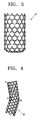
- FIG. 3 shows a carbon nanotube according to an embodiment of the present invention.
- a carbon nanotube 21 according to an embodiment of the present invention has C-H chemical bonds formed by binding hydrogen atoms to dangling bonds on its surface.
- the carbon nanotube 21 can be manufactured using, for example, arc discharge, laser vaporization, plasma enhanced chemical vapor deposition (PECVD), thermal chemical vapor deposition, vapor phase growth, and the like.
- PECVD plasma enhanced chemical vapor deposition
- thermal chemical vapor deposition thermal chemical vapor deposition, vapor phase growth, and the like.
- Carbon nanotubes according to the present invention have chemical bonds between their carbon atoms and hydrogen atoms, in which sp 3 hybrid bonding is promoted while sp 2 hybrid bonding is suppressed to take energy away from the Fermi level electrons, thereby giving the carbon nanotubes semiconductor properties.
- Carbon atoms whose atomic number is 6, have an electron configuration of 1 s 2 2 s 2 2 p 2 in the ground state. However, the electron configuration of carbon is converted when covalently bonded to another atom. In other words, after one of the electrons in the 2 s orbital is promoted to the 2 p orbital, the 2 s orbital and the 2 p orbital are combined to give sp hybrid orbitals.
- An sp hybrid orbital is formed from one s orbital and one p orbital with electrons
- three sp 2 hybrid orbitals are formed from one s orbital and two p orbitals with electrons
- four sp 3 hybrid orbitals are formed from one s orbital and three p orbitals with electrons.
- the electron configuration of carbon atoms enabling them to form a crystalline structure on their own includes sp 3 and sp 2 configurations.
- the sp 3 configuration with four hybrid orbitals permits carbon atoms to form four strong ⁇ bonds.
- the sp 2 configuration with three hybrid orbitals permits carbon atoms to form three ⁇ bonds in a plane, which are weaker than those in the sp 3 configuration.
- the sp 2 configuration also permits the electrons in the p orbitals to form weak ⁇ bonds.
- Carbon nanotubes according to the present invention are synthesized by forming C-H chemical bonds through the addition of hydrogen into carbon nanotubes having the sp 3 and sp 2 electron configurations, in which ⁇ or ⁇ * bonds near the Fermi level in the sp 2 hybrid orbitals are cleaved, so that less sp 2 bonds and more sp 3 bonds are present in the structure of the carbon nanotubes.
- the hydrogen and carbon atoms form a strong C-H bond with an atomic binding energy of -2.65 eV, and C-C bonds in the carbon nanotubes have a bond length of about 1.54 ⁇ , which is almost equal to that of diamond.
- the C-C bond remains resistant to external environmental variations or strong electrical current and thus prevents decomposition of the carbon nanotubes.
- the carbon nanotubes according to an embodiment of the present invention functionalized by hydrogen have semiconductor properties that are essential for them to be applied to nanotransistors.
- Nanotransistors can be manufactured using the functional hydrogenated carbon nanotubes with an improved yield of almost 100%. Also, the nanotransistors are workable at high temperature due to the stable C-H chemical bonds.
- FIG. 4 shows the configuration of an intermolecular junction device manufactured using carbon nanotubes, according to an embodiment of the present invention.
- intermolecular junction devices are molecular diode devices manufactured by kinking carbon nanotubes, with one metallic kinked end and the other a semiconductor end.
- the intermolecular junction device shown in FIG. 4 has a heterogeneous structure of two kinds of carbon nanotubes, wherein carbon nanotubes functionalized by hydrogen according to the present invention may be used for at least one of the carbon nanotubes.
- the two carbon nanotubes are bound together with different chiral angles at binding sites 5 and 7.
- Heterogeneous carbon nanotubes having different energy bandgaps which can thus be used for diodes, can be manufactured by the hydrogenation of a portion of carbon nanotubes.
- carbon nanotubes having properties required for such a device can be manufactured by partial hydrogenation of arbitrary carbon nanotubes.
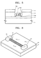
- FIG. 5 is a sectional view of a field emitter device using carbon nanotubes according to an embodiment of the present invention.
- a field emitter device includes a source electrode 12 formed on a substrate 11 as a stripe, a thin film formed on the source electrode 12 with tips 15 of carbon nanotubes functionalized by hydrogen, a gate dielectric layer 13 formed to surround the tips 15, and a gate electrode 14 formed on the gate dielectric layer 13 with an opening 14a above the tips 15 for electron emission.
- a drain electrode (not shown) is formed on the gate electrode 14 as a stripe perpendicular to the source electrode 13.
- an electron emitter source for the field emitter be manufactured by controlling the electronic energy bandgap of carbon nanotubes for uniform resistance, and be applied uniformly over the entire area of the field emitter for uniform electron emission.
- FIG. 6 is a perspective view of a nanotransistor using carbon nanotubes according to an embodiment of the present invention.
- a nanotransistor using carbon nanotubes according to an embodiment of the present invention includes a substrate 21, an insulating layer 23 formed on the substrate 21, a source region 25 and a drain region 27 formed on the insulating layer 23 with a separation distance therebetween, and a carbon nanotube unit 31 connecting the source region 25 and the drain region 27 as an electron channel.
- the carbon nanotube unit 31 in the nanotransistor is formed of a semiconductor carbon nanotube fabricated by hydrogen functionalization according to the present invention.
- the energy bandgap of the carbon nanotube for the unit 31 can be controlled within a desired range by varying the duration for which and pressure under which source carbon nanotubes are exposed to hydrogen gas during hydrogenation.
- the semiconductor carbon nanotubes according to the embodiment of the present invention can be applied to memory devices, sensors, and the like as well as nanotransistors.
- the nanotransistor is described as having the source region 25 and the drain region 27 on the substrate 21, the source region 25 and the drain region 27 may be located in the substrate 21.
- the carbon nanotube unit 31 is located in or on the substrate 21 to connect the source region 25 and the drain region 27.
- the substrate 21 is a silicon substrate, and the insulating layer 23 on the silicon substrate 21 is formed of silicon oxide.
- the source region 25 and the drain region 27 may be formed of metal such as titanium, gold, etc.
- the nanotransistor having such a configuration is formed using known semiconductor manufacturing processes such as photolithography, etching, oxidation, and thin film deposition.
- the semiconductor carbon nanotubes fabricated by hydrogen functionalization according to the embodiment of the present invention can be applied as probe tips for scanning probe microscopy (SPM), as well as the nanodevices illustrated in FIGS. 4 and 6, and further for nanobalances using the resonance of nanotubes, electro-optic devices using the optical nature of carbon nanotubes, various electronic devices, memory devices, chemical sensors using field effect transistors, and the like.
- SPM scanning probe microscopy
- the H of the C-H bond on the carbon nanotube wall may be replaced by another substitutent in order for the carbon nanotubes to be used for biochips or biosensors.
- the carbon nanotubes may be dispersed in a solution to increase their electronegativity and surface area for use as energy devices such as surface capacitors.
- FIG. 7 is a flowchart illustrating a method for manufacturing hydrogenated carbon nanotubes according to an embodiment of the present invention.
- FIG. 8 shows an apparatus for carbon nanotube hydrogenation.
- a substrate 45 with carbon nanotube powder or individual carbon nanotubes thereon is heated in a vacuum container 43 at 10 -6 torr or less, above 100°C for 2 hours or longer, to remove gas adsorbed on the walls of the carbon nanotubes (step 101).
- a tungsten filament 49 disposed near the top entrance of the vacuum container, which is heated to a temperature 1500°C or greater by an electric current, a RF or DC bias voltage is applied to hydrogen gas in molecular form supplied through an inlet 47, or an arc discharge is induced to dissociate the molecular hydrogen gas into hydrogen atoms (step 103).
- the dissociated hydrogen atoms contact and are adsorbed into the walls of the carbon nanotubes to form C-H chemical bonds (step 105).
- the temperature of the substrate 45 is maintained at 100°C or less.
- the duration for which the carbon nanotubes are exposed to the hydrogen gas is controlled within a range of from 1 hour to 20 hours, and the pressure of the hydrogen gas in the vacuum container is controlled within a range from 10 -6 torr to 10 -3 torr, such that metallic carbon nanotubes are converted into semiconductor nanotubes or narrow energy bandgap semiconductor carbon nanotubes are converted into wide energy bandgap semiconductor carbon nanotubes.
- FIG. 9A is a scanning electron microscopic (SEM) image showing the hydrogenation of carbon nanotubes to form C-H bonds in the manufacture of semiconductor carbon nanotubes by hydrogenation according to the present invention.
- the carbon nanotubes are bound to the silicon substrate by metal using electron-beam lithography, wherein half of a carbon nanotube is buried in a silicon oxide (SiO 2 ) layer having a thickness of 100 nm while the other half is exposed to the hydrogen gas, as shown in FIG. 9A.
- a vacuum atmosphere is created by degassing at 300°C for 6 hours, and the carbon nanotubes are hydrogenated by being exposed to the hydrogen gas at a temperature of 100°C and a pressure of 10 -5 torr for several hours.
- the atoms of the carbon nanotube are carbon atoms
- the smaller atoms on the external wall of the carbon nanotube are hydrogen atoms.
- FIG. 9B is a graph of current versus voltage for pristine samples (denoted as "MS”) and semiconducting samples (denoted as "SS”) having an energy bandgap of 0.8 eV before hydrogenation
- FIG. 9B is a graph of current versus voltage for the MS and SS after hydrogenation.
- the pristine samples have metallic properties at room temperature, and the MS and SS have resistances of 155 k ⁇ and 10 M ⁇ , respectively.
- the MS and SS are converted, by hydrogenation, into semiconductor carbon nanotubes with a wide energy bandgap, with a rectifying effect at an ambient temperature that is greater in the SS than in the MS.
- the insert in FIG. 9C is a curve for the pristine MS sample showing differential conductance (dI/dV) at 5.6K with respect to drain voltage before hydrogenation
- FIG. 9C is a curve for the MS showing differential conductance (dI/dV) at 4.2K with respect to drain voltage after hydrogenation.
- the MS before hydrogenation has a value (dI/dV) of differential conductance at a zero-drain voltage, i.e., in a zero bias region, at 5.6K, which indicates that the MS has conductance and is nearly metallic.
- the graph of FIG. 9C shows that the MS becomes semiconductive with a widened energy bandgap of about 1. 88eV after hydrogenation and that the conductance of the MS linearly increases beyond the energy bandgap region.
- the insert in FIG. 9D is a curve for the pristine SS sample showing differential conductance (dI/dV) at 5.6K with respect to drain voltage before hydrogenation
- FIG. 9D is a curve for the SS sample showing differential conductance at 4.2K with respect to drain voltage after hydrogenation.
- the SS before hydrogenation has semiconductor properties with an energy bandgap of about 0.8 eV.
- the graph of FIG. 9D shows that the SS after hydrogenation has improved semiconductor properties with a widened energy bandgap of about 4.4 eV.
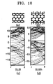
- FIG. 10 illustrates the conversion of metallic carbon nanotubes into semiconducting carbon nanotubes by hydrogenation according to the present invention, in which changes in configuration and energy bandgap before and after hydrogenation are shown.
- FIG. 10 shows the configuration of a (5,5) armchair metallic sample
- (b) shows the configuration of a (5,5)h semiconducting sample hydrogenated from the (5,5) armchair metallic sample
- (c) shows the energy level of the (5,5) metallic sample of (a)
- (d) shows the energy level of the (5,5)h semiconducting sample of (b).
- the (5,5) metallic sample was converted into the semiconducting sample (b) having an energy bandgap of 1.63 eV after hydrogenation.
- FIG. 11 illustrates the conversion of a (9,0) zigzag semiconducting sample having a narrow energy bandgap into a (9,0)h semiconducting sample having a wide energy bandgap by hydrogenation according to the present invention, in which changes in configuration and energy bandgap before and after hydrogenation are shown.
- FIG. 11 shows the configuration of a (9,0) semiconducting sample
- (b) shows the configuration of a (9,0)h semiconducting sample
- (c) shows the energy level of the (9,0) semiconducting sample of (a) having a zero energy bandgap
- (d) shows the energy level of the (9,0)h semiconductor carbon nanotube of (b) having a relatively wide energy bandgap.
- FIGS. 12A and 13A shows intermolecular junctions between general carbon nanotubes and hydrogenated carbon nanotubes according to the present invention.
- the length of C-CH bonds is 1.48 ⁇ . However, the length of all other bonds from the second layer at the interface layer on both sides is closer to the length of individual tubes.
- Carbon atoms of the metallic carbon nanotube located at the hydrogenated carbon nanotube side accept extra charges from the adsorbed hydrogen atoms of the hydrogenated carbon nanotube, rather than from carbon atoms at the metallic CNT side, so that more charges accumulate at the interface layer closer to the metallic carbon nanotube than the semiconductor hydrogenated carbon nanotube. Accordingly, a small degree of band-bending is highly likely to occur in the MS junction, whereas those in the SS junction are negligible.
- FIGS. 12B and 13B show the height and energy bandgap of a M-S Schottky junction barrier formed by connecting the MS and the SS, and the height and energy bandgap of an S-S Schottky junction barrier formed by connecting two SSs, respectively.
- FIGS. 12B and 13B show junction band diagrams for the M-S and S-S junctions, respectively, where the junction barrier height is equal to the energy band offset.
- the energy bandgap between a valence band (VB) and a conduction band (CB) in a semiconductor carbon nanotube region reaches 1.88 eV, and there is a relatively low energy barrier between the metallic carbon nanotube (MS) and the SS.
- FIG. 13B which is for the case where a semiconductor carbon nanotube (SS) having a relatively wide energy bandgap of 4.4 eV is connected with a semiconductor carbon nanotube (SS) having a narrow energy bandgap of 0.8 eV, apparently, the energy bandgap becomes wide with an energy barrier of 3.6 eV between the two SSs.
- the M-S and S-S junctions are hole-doped, and an abrupt junction occurs in the interface region of one or two monolayers.
- charges may transfer from the MS sample to the SS sample, thereby inducing a sharp band-bending in the region of semiconductor carbon nanotubes.
- the migration of charges in the S-S junction is negligible, the charge transfer in the S-S junction may cause a spike.
- FIGS. 14A and 14B are graphs of current versus voltage for carbon nanotubes MS and SS before and after hydrogenation, respectively.
- a pristine MS and a pristine SS having a narrow energy bandgap show a linear, proportional current-to-voltage relation which indicates that the pristine MS and SS have metallic properties and a metal-like nature, respectively.
- the MS and the SS having the narrow energy bandgap have a rectifying effect like semiconductors having a large energy bandgap.
- FIGS. 15A and 15B show graphs of current versus voltage before and after hydrogenation, respectively, in field effect transistors (FETs).
- FIG. 15A is a graph of source-drain (? ) current I d at 5.6K with respect to gate voltage V g in a FET having an electron channel formed using a non-hydrogenated metallic carbon nanotube (MC).
- the source-drain current I d is about -500 nA at a drain voltage V d of -0.27V and about 500 nA at a drain voltage V d of 0.27V.
- the source-drain current I d of the FET is constant regardless of gate voltage ( V g ) variations. This means that the FET operates inappropriately as a transistor and that the MC acts merely as a metallic tube in the FET.
- FIG. 15B is a graph of source-drain current I d at 287K with respect to gate voltage V g in a FET formed using hydrogenated multi-wall carbon nanotubes.
- the drain voltage is positive, i.e., when a positive bias voltage is applied to the hydrogenated carbon nanotubes, a large current flows across the transistor.
- the drain voltage is negative, current is suppressed, and a rectifying effect appears.
- the source-drain current I d increases as the gate voltage V g increases. Therefore, the FET properly and stably operates as a transistor at an ambient temperature, irrespective of temperature variations. This result supports that an asymmetric metal-semiconductor (MS) junction has been formed between the hydrogenated carbon nanotubes and non-hydrogenated metallic carbon nanotubes in the FET.
- MS metal-semiconductor
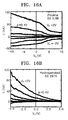
- FIG. 16A is a graph of drain current versus gate voltage at a predetermined drain voltage for the pristine SS sample before hydrogenation.
- the non-hydrogenated semiconductor carbon nanotubes show semiconductor properties with a gate effect at low temperature.
- the flow of a limited amount of current at a zero gate voltage means that the carbon nanotubes are already hole-doped, and the small anisotropy in current at drain voltages of different polarities means that the carbon nanotubes and a metal electrode are in asymmetrical contact.
- FIG. 16B is a graph of source-drain current versus gate voltage at a predetermined drain voltage for the SS sample after hydrogenation.
- the SS sample after hydrogenation, the SS sample has a large energy bandgap, thereby providing an about 10 times greater rectifying effect than before hydrogenation. It can be expected from this result that an S-S junction between the narrow-bandgap and wide-bandgap semiconductor nanotubes has been formed in the SS sample by hydrogenation.
- the junction barrier height after hydrogenation is greater in the metallic carbon nanotube at 1 eV than in the semiconductor carbon nanotube at 0.35 eV.
- the energy bandgap of the carbon nanotubes can be easily controlled by varying the duration and temperature of hydrogenation, so that the conversion of metallic carbon nanotubes into semiconductor carbon nanotubes and of semiconductor carbon nanotubes having a relatively narrow energy bandgap into semiconductor carbon nanotubes having a relatively wide energy bandgap can be achieved.
- Such hydrogenated carbon nanotubes according to the present invention have a wide range of applications including, for example, use in various electronic devices, optoelectronic devices, energy storage devices, and the like, and particularly, can be used for nanotransistors workable at high temperature because the hydrogenated carbon nanotubes according to the present invention have stable C-H and C-C chemical bonds.
Landscapes
- Chemical & Material Sciences (AREA)
- Engineering & Computer Science (AREA)
- Nanotechnology (AREA)
- Materials Engineering (AREA)
- Crystallography & Structural Chemistry (AREA)
- Organic Chemistry (AREA)
- Physics & Mathematics (AREA)
- Condensed Matter Physics & Semiconductors (AREA)
- General Physics & Mathematics (AREA)
- Inorganic Chemistry (AREA)
- Manufacturing & Machinery (AREA)
- Composite Materials (AREA)
- Mathematical Physics (AREA)
- Theoretical Computer Science (AREA)
- Carbon And Carbon Compounds (AREA)
- Thin Film Transistor (AREA)
- Organic Low-Molecular-Weight Compounds And Preparation Thereof (AREA)
- Cold Cathode And The Manufacture (AREA)
Applications Claiming Priority (2)
| Application Number | Priority Date | Filing Date | Title |
|---|---|---|---|
| KR2002024476 | 2002-05-03 | ||
| KR1020020024476A KR100571803B1 (ko) | 2002-05-03 | 2002-05-03 | 수소로 기능화된 반도체 탄소나노튜브를 포함하는 전자 소자 및 그 제조방법 |
Publications (3)
| Publication Number | Publication Date |
|---|---|
| EP1359122A2 true EP1359122A2 (de) | 2003-11-05 |
| EP1359122A3 EP1359122A3 (de) | 2005-06-22 |
| EP1359122B1 EP1359122B1 (de) | 2012-09-05 |
Family
ID=29208778
Family Applications (1)
| Application Number | Title | Priority Date | Filing Date |
|---|---|---|---|
| EP03252763A Expired - Lifetime EP1359122B1 (de) | 2002-05-03 | 2003-05-01 | Verfahren zur Vergrößerung der Bandlücke von Kohlenstoff-Nanoröhren mit Wasserstoff Funktionalisierung |
Country Status (5)
| Country | Link |
|---|---|
| US (3) | US20030205457A1 (de) |
| EP (1) | EP1359122B1 (de) |
| JP (1) | JP2004002409A (de) |
| KR (1) | KR100571803B1 (de) |
| CN (1) | CN100421202C (de) |
Cited By (1)
| Publication number | Priority date | Publication date | Assignee | Title |
|---|---|---|---|---|
| EP1753902A4 (de) * | 2004-04-27 | 2011-04-27 | Nanosource Inc | Systeme und verfahren zur herstellungvon nanoröhrchenstrukturen |
Families Citing this family (59)
| Publication number | Priority date | Publication date | Assignee | Title |
|---|---|---|---|---|
| US6723299B1 (en) | 2001-05-17 | 2004-04-20 | Zyvex Corporation | System and method for manipulating nanotubes |
| US20040034177A1 (en) | 2002-05-02 | 2004-02-19 | Jian Chen | Polymer and method for using the polymer for solubilizing nanotubes |
| US6905667B1 (en) | 2002-05-02 | 2005-06-14 | Zyvex Corporation | Polymer and method for using the polymer for noncovalently functionalizing nanotubes |
| KR100827861B1 (ko) | 2003-05-22 | 2008-05-07 | 지벡스 퍼포먼스 머티리얼즈, 엘엘씨 | 나노복합물 및 이의 제조 방법 |
| US7329902B2 (en) * | 2003-06-11 | 2008-02-12 | Stmicroelectronics S.R.L. | IR-light emitters based on SWNT's (single walled carbon nanotubes), semiconducting SWNTs-light emitting diodes and lasers |
| US7038299B2 (en) * | 2003-12-11 | 2006-05-02 | International Business Machines Corporation | Selective synthesis of semiconducting carbon nanotubes |
| US7135773B2 (en) * | 2004-02-26 | 2006-11-14 | International Business Machines Corporation | Integrated circuit chip utilizing carbon nanotube composite interconnection vias |
| US7296576B2 (en) | 2004-08-18 | 2007-11-20 | Zyvex Performance Materials, Llc | Polymers for enhanced solubility of nanomaterials, compositions and methods therefor |
| KR100635546B1 (ko) * | 2004-12-24 | 2006-10-17 | 학교법인 포항공과대학교 | 전계 효과 트랜지스터 채널 구조를 갖는 스캐닝 프로브마이크로 스코프의 탐침 및 그 제조 방법 |
| US7989349B2 (en) | 2005-04-15 | 2011-08-02 | Micron Technology, Inc. | Methods of manufacturing nanotubes having controlled characteristics |
| TWI287041B (en) * | 2005-04-27 | 2007-09-21 | Jung-Tang Huang | An ultra-rapid DNA sequencing method with nano-transistors array based devices |
| JP4706066B2 (ja) | 2005-08-19 | 2011-06-22 | 独立行政法人産業技術総合研究所 | 電気化学キャパシタ及びそれに用いる電極材料 |
| KR101082440B1 (ko) | 2005-10-04 | 2011-11-11 | 삼성에스디아이 주식회사 | 전자 방출 소자, 이를 구비한 전자 방출 디스플레이 장치및 그 제조 방법 |
| GB2434692A (en) * | 2005-12-29 | 2007-08-01 | Univ Surrey | Photovoltaic or electroluminescent devices with active region comprising a composite polymer and carbon nanotube material. |
| US8758717B2 (en) * | 2006-10-19 | 2014-06-24 | Rensselaer Polytechnic Institute | Electrical current-induced structural changes and chemical functionalization of carbon nanotubes |
| US20080093693A1 (en) * | 2006-10-20 | 2008-04-24 | Kamins Theodore I | Nanowire sensor with variant selectively interactive segments |
| US9806273B2 (en) * | 2007-01-03 | 2017-10-31 | The United States Of America As Represented By The Secretary Of The Army | Field effect transistor array using single wall carbon nano-tubes |
| US8297351B2 (en) * | 2007-12-27 | 2012-10-30 | Schlumberger Technology Corporation | Downhole sensing system using carbon nanotube FET |
| JP5369663B2 (ja) | 2008-01-31 | 2013-12-18 | Jfeスチール株式会社 | 加工性に優れた高強度溶融亜鉛めっき鋼板およびその製造方法 |
| JP4843077B2 (ja) * | 2008-12-03 | 2011-12-21 | 韓國電子通信研究院 | トランジスタ構造のバイオセンサー及びその製造方法 |
| US20100284903A1 (en) | 2009-05-11 | 2010-11-11 | Honda Patents & Technologies North America, Llc | New Class of Tunable Gas Storage and Sensor Materials |
| US8569900B2 (en) * | 2009-07-20 | 2013-10-29 | Hewlett-Packard Development Company, L.P. | Nanowire sensor with angled segments that are differently functionalized |
| US8691145B2 (en) | 2009-11-16 | 2014-04-08 | Flodesign Sonics, Inc. | Ultrasound and acoustophoresis for water purification |
| WO2011115891A2 (en) * | 2010-03-15 | 2011-09-22 | University Of Florida Research Foundation Inc. | Graphite and/or graphene semiconductor devices |
| US9012904B2 (en) * | 2011-03-25 | 2015-04-21 | Semiconductor Energy Laboratory Co., Ltd. | Semiconductor device and method for manufacturing the same |
| US9219159B2 (en) | 2011-03-25 | 2015-12-22 | Semiconductor Energy Laboratory Co., Ltd. | Method for forming oxide semiconductor film and method for manufacturing semiconductor device |
| TWI545652B (zh) | 2011-03-25 | 2016-08-11 | 半導體能源研究所股份有限公司 | 半導體裝置及其製造方法 |
| US9458450B2 (en) | 2012-03-15 | 2016-10-04 | Flodesign Sonics, Inc. | Acoustophoretic separation technology using multi-dimensional standing waves |
| US9752113B2 (en) | 2012-03-15 | 2017-09-05 | Flodesign Sonics, Inc. | Acoustic perfusion devices |
| US9745548B2 (en) | 2012-03-15 | 2017-08-29 | Flodesign Sonics, Inc. | Acoustic perfusion devices |
| US10689609B2 (en) | 2012-03-15 | 2020-06-23 | Flodesign Sonics, Inc. | Acoustic bioreactor processes |
| US10953436B2 (en) | 2012-03-15 | 2021-03-23 | Flodesign Sonics, Inc. | Acoustophoretic device with piezoelectric transducer array |
| US10704021B2 (en) | 2012-03-15 | 2020-07-07 | Flodesign Sonics, Inc. | Acoustic perfusion devices |
| US9950282B2 (en) | 2012-03-15 | 2018-04-24 | Flodesign Sonics, Inc. | Electronic configuration and control for acoustic standing wave generation |
| US10967298B2 (en) | 2012-03-15 | 2021-04-06 | Flodesign Sonics, Inc. | Driver and control for variable impedence load |
| US9567559B2 (en) | 2012-03-15 | 2017-02-14 | Flodesign Sonics, Inc. | Bioreactor using acoustic standing waves |
| US10322949B2 (en) | 2012-03-15 | 2019-06-18 | Flodesign Sonics, Inc. | Transducer and reflector configurations for an acoustophoretic device |
| US9272234B2 (en) | 2012-03-15 | 2016-03-01 | Flodesign Sonics, Inc. | Separation of multi-component fluid through ultrasonic acoustophoresis |
| US10370635B2 (en) | 2012-03-15 | 2019-08-06 | Flodesign Sonics, Inc. | Acoustic separation of T cells |
| US10737953B2 (en) | 2012-04-20 | 2020-08-11 | Flodesign Sonics, Inc. | Acoustophoretic method for use in bioreactors |
| KR101297274B1 (ko) * | 2013-02-28 | 2013-08-20 | 주식회사 엔디디 | 바이오 센서 및 그 제조 방법 |
| US9745569B2 (en) | 2013-09-13 | 2017-08-29 | Flodesign Sonics, Inc. | System for generating high concentration factors for low cell density suspensions |
| WO2015105955A1 (en) | 2014-01-08 | 2015-07-16 | Flodesign Sonics, Inc. | Acoustophoresis device with dual acoustophoretic chamber |
| US9744483B2 (en) | 2014-07-02 | 2017-08-29 | Flodesign Sonics, Inc. | Large scale acoustic separation device |
| US10106770B2 (en) | 2015-03-24 | 2018-10-23 | Flodesign Sonics, Inc. | Methods and apparatus for particle aggregation using acoustic standing waves |
| US11708572B2 (en) | 2015-04-29 | 2023-07-25 | Flodesign Sonics, Inc. | Acoustic cell separation techniques and processes |
| US11377651B2 (en) | 2016-10-19 | 2022-07-05 | Flodesign Sonics, Inc. | Cell therapy processes utilizing acoustophoresis |
| US11021699B2 (en) | 2015-04-29 | 2021-06-01 | FioDesign Sonics, Inc. | Separation using angled acoustic waves |
| US11459540B2 (en) | 2015-07-28 | 2022-10-04 | Flodesign Sonics, Inc. | Expanded bed affinity selection |
| US11474085B2 (en) | 2015-07-28 | 2022-10-18 | Flodesign Sonics, Inc. | Expanded bed affinity selection |
| JP6582759B2 (ja) | 2015-09-02 | 2019-10-02 | 富士通株式会社 | 電子デバイス及びその製造方法 |
| US10710006B2 (en) | 2016-04-25 | 2020-07-14 | Flodesign Sonics, Inc. | Piezoelectric transducer for generation of an acoustic standing wave |
| US11214789B2 (en) | 2016-05-03 | 2022-01-04 | Flodesign Sonics, Inc. | Concentration and washing of particles with acoustics |
| US11085035B2 (en) | 2016-05-03 | 2021-08-10 | Flodesign Sonics, Inc. | Therapeutic cell washing, concentration, and separation utilizing acoustophoresis |
| CN109715124B (zh) | 2016-05-03 | 2022-04-22 | 弗洛设计声能学公司 | 利用声泳的治疗细胞洗涤、浓缩和分离 |
| WO2018075830A1 (en) | 2016-10-19 | 2018-04-26 | Flodesign Sonics, Inc. | Affinity cell extraction by acoustics |
| KR102439221B1 (ko) | 2017-12-14 | 2022-09-01 | 프로디자인 소닉스, 인크. | 음향 트랜스듀서 구동기 및 제어기 |
| KR102488299B1 (ko) * | 2020-10-28 | 2023-01-13 | 숭실대학교산학협력단 | 구조적 안정성이 향상된 탄소나노튜브 시트 롤 이미터, 이의 제조방법 및 이를 이용한 전계 방출 소자 |
| WO2025183765A2 (en) * | 2023-11-24 | 2025-09-04 | Massachusetts Institute Of Technology | Remote-contact catalysis for high-purity semiconducting carbon nanotube array |
Family Cites Families (14)
| Publication number | Priority date | Publication date | Assignee | Title |
|---|---|---|---|---|
| US6538262B1 (en) * | 1996-02-02 | 2003-03-25 | The Regents Of The University Of California | Nanotube junctions |
| US5858477A (en) * | 1996-12-10 | 1999-01-12 | Akashic Memories Corporation | Method for producing recording media having protective overcoats of highly tetrahedral amorphous carbon |
| JP3136334B2 (ja) * | 1997-07-23 | 2001-02-19 | 工業技術院長 | カーボンナノチューブの製造方法 |
| US6280677B1 (en) * | 1997-11-05 | 2001-08-28 | North Carolina State University | Physical property modification of nanotubes |
| KR100277881B1 (ko) | 1998-06-16 | 2001-02-01 | 김영환 | 트랜지스터 |
| US6159538A (en) * | 1999-06-15 | 2000-12-12 | Rodriguez; Nelly M. | Method for introducing hydrogen into layered nanostructures |
| JP4405650B2 (ja) * | 1999-07-13 | 2010-01-27 | 日機装株式会社 | 炭素質ナノチューブ、繊維集合体及び炭素質ナノチューブの製造方法 |
| KR19990073590A (ko) * | 1999-07-27 | 1999-10-05 | 이철진 | 플라즈마 화학기상증착법에 의한 고순도 탄소나노튜브의 대량합성. |
| JP2001180920A (ja) | 1999-12-24 | 2001-07-03 | Nec Corp | ナノチューブの加工方法及び電界放出型冷陰極の製造方法並びに表示装置の製造方法 |
| KR100372307B1 (ko) | 2000-05-01 | 2003-02-17 | 주식회사 퀀텀테크인터내셔날 | 티올기가 부착된 탄소나노튜브 및 이의 제조방법 |
| JP2002025425A (ja) * | 2000-07-07 | 2002-01-25 | Hitachi Ltd | 電子エミッターとその製造法および電子線装置 |
| US6752977B2 (en) * | 2001-02-12 | 2004-06-22 | William Marsh Rice University | Process for purifying single-wall carbon nanotubes and compositions thereof |
| WO2002103737A2 (en) * | 2001-06-14 | 2002-12-27 | Hyperion Catalysis International, Inc. | Field emission devices using ion bombarded carbon nanotubes |
| EP1513621A4 (de) * | 2002-05-21 | 2005-07-06 | Eikos Inc | Verfahren zur mustererstellung auf kohlenstoffnanoröhrenüberzügen und kohlenstoffnanoröhrenverdrahtung |
-
2002
- 2002-05-03 KR KR1020020024476A patent/KR100571803B1/ko not_active Expired - Lifetime
-
2003
- 2003-05-01 EP EP03252763A patent/EP1359122B1/de not_active Expired - Lifetime
- 2003-05-01 JP JP2003126118A patent/JP2004002409A/ja active Pending
- 2003-05-03 CN CNB031454240A patent/CN100421202C/zh not_active Expired - Lifetime
- 2003-05-05 US US10/428,835 patent/US20030205457A1/en not_active Abandoned
-
2006
- 2006-01-09 US US11/327,368 patent/US7326605B2/en not_active Expired - Fee Related
-
2008
- 2008-01-31 US US12/023,475 patent/US8658484B2/en not_active Expired - Fee Related
Non-Patent Citations (5)
| Title |
|---|
| KEUN SOO KIM ET AL: "Band gap modulation of a carbon nanotube by hydrogen functionalization" JOURNAL OF THE KOREAN PHYSICAL SOCIETY KOREAN PHYS. SOC SOUTH KOREA, vol. 42, February 2003 (2003-02), pages S137-S142, XP002326109 ISSN: 0374-4884 * |
| KEUN SOO KIM ET AL: "MODIFICATION OF ELECTRONIC STRUCTURES OF A CARBON NANOTUBE BY HYDROGEN FUNCTIONALIZATION" ADVANCED MATERIALS, VCH VERLAGSGESELLSCHAFT, WEINHEIM, DE, vol. 24, no. 14, 17 December 2002 (2002-12-17), pages 1818-1821, XP001141105 ISSN: 0935-9648 * |
| KHARE B N ET AL: "Functionalization of carbon nanotubes using atomic hydrogen from a glow discharge" NANO LETTERS AMERICAN CHEM. SOC USA, vol. 2, no. 1, January 2002 (2002-01), pages 73-77, XP002326111 ISSN: 1530-6984 * |
| MICKELSON E T ET AL: "FLUORINATION OF SINGLE-WALL CARBON NANOTUBES" CHEMICAL PHYSICS LETTERS, NORTH-HOLLAND, AMSTERDAM, NL, vol. 296, 30 October 1998 (1998-10-30), pages 188-194, XP000864355 ISSN: 0009-2614 * |
| PEKKER S. ET AL: "Hydrogenation of carbon nanotubes and graphite in liquid ammonia" J. PHYS. CHEM. B, vol. 105, 26 July 2001 (2001-07-26), pages 7938-7943, XP002326110 * |
Cited By (1)
| Publication number | Priority date | Publication date | Assignee | Title |
|---|---|---|---|---|
| EP1753902A4 (de) * | 2004-04-27 | 2011-04-27 | Nanosource Inc | Systeme und verfahren zur herstellungvon nanoröhrchenstrukturen |
Also Published As
| Publication number | Publication date |
|---|---|
| US20080181838A1 (en) | 2008-07-31 |
| US8658484B2 (en) | 2014-02-25 |
| KR100571803B1 (ko) | 2006-04-17 |
| US7326605B2 (en) | 2008-02-05 |
| KR20030086104A (ko) | 2003-11-07 |
| JP2004002409A (ja) | 2004-01-08 |
| EP1359122A3 (de) | 2005-06-22 |
| EP1359122B1 (de) | 2012-09-05 |
| CN100421202C (zh) | 2008-09-24 |
| US20060237708A1 (en) | 2006-10-26 |
| CN1459815A (zh) | 2003-12-03 |
| US20030205457A1 (en) | 2003-11-06 |
Similar Documents
| Publication | Publication Date | Title |
|---|---|---|
| EP1359122B1 (de) | Verfahren zur Vergrößerung der Bandlücke von Kohlenstoff-Nanoröhren mit Wasserstoff Funktionalisierung | |
| TWI463654B (zh) | 奈米管/奈米導線場效電晶體之自行對準製程 | |
| Wang et al. | Synthesis and device applications of high-density aligned carbon nanotubes using low-pressure chemical vapor deposition and stacked multiple transfer | |
| Graham et al. | How do carbon nanotubes fit into the semiconductor roadmap? | |
| Weitz et al. | High-performance carbon nanotube field effect transistors with a thin gate dielectric based on a self-assembled monolayer | |
| McGill et al. | High-performance, hysteresis-free carbon nanotube field-effect transistors via directed assembly | |
| TWI780037B (zh) | 電子純碳奈米管油墨及其識別方法,以及製成一電子純碳奈米管薄膜之方法 | |
| Kim et al. | Cutting of multiwalled carbon nanotubes by a negative voltage tip of an atomic force microscope: A possible mechanism | |
| Jacobberger et al. | High-performance charge transport in semiconducting armchair graphene nanoribbons grown directly on germanium | |
| Rawlett et al. | A molecular electronics toolbox | |
| CN102354668B (zh) | 一种碳基纳米材料晶体管的制备方法 | |
| US20110268884A1 (en) | Formation of nanoscale carbon nanotube electrodes using a self-aligned nanogap mask | |
| US20070246364A1 (en) | Selectively placing catalytic nanoparticles of selected size for nanotube and nanowire growth | |
| JP6659956B2 (ja) | ショットキーバリアダイオード及び電子装置 | |
| JP4904696B2 (ja) | 電界効果トランジスタおよびその製造方法 | |
| CN101252145B (zh) | 一种碳纳米管纳电子器件及其制备方法 | |
| US20080296558A1 (en) | Method of Synthesizing Y-Junction Single-Walled Carbon Nanotubes and Products Formed Thereby | |
| Talin et al. | Assembly and electrical characterization of DNA-wrapped carbon nanotube devices | |
| Albrecht et al. | Scanning tunnelling spectroscopy and ab initio calculations of single-walled carbon nanotubes interfaced with highly doped hydrogen-passivated Si (100) substrates | |
| Valentin et al. | Self-assembly fabrication of high performance carbon nanotubes based FETs | |
| Aikawa et al. | Facile fabrication of all-SWNT field-effect transistors | |
| US11211560B2 (en) | Self-assembly of nanostructures | |
| EP1667238A1 (de) | Verfahren zur herstellung eines feldeffekt-halbleiterbauelements | |
| US20100068828A1 (en) | Method of forming a structure having a giant resistance anisotropy or low-k dielectric | |
| Zhang | A study on gate oxide and extension region of carbon nanotube field effect transistor |
Legal Events
| Date | Code | Title | Description |
|---|---|---|---|
| PUAI | Public reference made under article 153(3) epc to a published international application that has entered the european phase |
Free format text: ORIGINAL CODE: 0009012 |
|
| AK | Designated contracting states |
Kind code of ref document: A2 Designated state(s): AT BE BG CH CY CZ DE DK EE ES FI FR GB GR HU IE IT LI LU MC NL PT RO SE SI SK TR |
|
| AX | Request for extension of the european patent |
Extension state: AL LT LV MK |
|
| PUAL | Search report despatched |
Free format text: ORIGINAL CODE: 0009013 |
|
| AK | Designated contracting states |
Kind code of ref document: A3 Designated state(s): AT BE BG CH CY CZ DE DK EE ES FI FR GB GR HU IE IT LI LU MC NL PT RO SE SI SK TR |
|
| AX | Request for extension of the european patent |
Extension state: AL LT LV MK |
|
| 17P | Request for examination filed |
Effective date: 20051109 |
|
| AKX | Designation fees paid |
Designated state(s): DE FR GB |
|
| 17Q | First examination report despatched |
Effective date: 20070219 |
|
| RIC1 | Information provided on ipc code assigned before grant |
Ipc: H01L 51/00 20060101ALI20111108BHEP Ipc: B82Y 10/00 20110101ALI20111108BHEP Ipc: C01B 31/02 20060101AFI20111108BHEP Ipc: B82Y 30/00 20110101ALI20111108BHEP |
|
| RTI1 | Title (correction) |
Free format text: METHOD FOR ENLARGING THE BANDGAP OF CARBON NANOTUBES BY HYDROGEN FUNCTIONALIZATION |
|
| GRAP | Despatch of communication of intention to grant a patent |
Free format text: ORIGINAL CODE: EPIDOSNIGR1 |
|
| GRAS | Grant fee paid |
Free format text: ORIGINAL CODE: EPIDOSNIGR3 |
|
| GRAA | (expected) grant |
Free format text: ORIGINAL CODE: 0009210 |
|
| AK | Designated contracting states |
Kind code of ref document: B1 Designated state(s): DE FR GB |
|
| REG | Reference to a national code |
Ref country code: GB Ref legal event code: FG4D |
|
| RAP2 | Party data changed (patent owner data changed or rights of a patent transferred) |
Owner name: SAMSUNG ELECTRONICS CO., LTD. |
|
| REG | Reference to a national code |
Ref country code: DE Ref legal event code: R096 Ref document number: 60342007 Country of ref document: DE Effective date: 20121025 |
|
| PLBE | No opposition filed within time limit |
Free format text: ORIGINAL CODE: 0009261 |
|
| STAA | Information on the status of an ep patent application or granted ep patent |
Free format text: STATUS: NO OPPOSITION FILED WITHIN TIME LIMIT |
|
| 26N | No opposition filed |
Effective date: 20130606 |
|
| REG | Reference to a national code |
Ref country code: DE Ref legal event code: R097 Ref document number: 60342007 Country of ref document: DE Effective date: 20130606 |
|
| REG | Reference to a national code |
Ref country code: FR Ref legal event code: PLFP Year of fee payment: 14 |
|
| REG | Reference to a national code |
Ref country code: DE Ref legal event code: R079 Ref document number: 60342007 Country of ref document: DE Free format text: PREVIOUS MAIN CLASS: C01B0031020000 Ipc: C01B0032050000 |
|
| REG | Reference to a national code |
Ref country code: FR Ref legal event code: PLFP Year of fee payment: 15 |
|
| REG | Reference to a national code |
Ref country code: FR Ref legal event code: PLFP Year of fee payment: 16 |
|
| PGFP | Annual fee paid to national office [announced via postgrant information from national office to epo] |
Ref country code: GB Payment date: 20220420 Year of fee payment: 20 Ref country code: FR Payment date: 20220425 Year of fee payment: 20 Ref country code: DE Payment date: 20220420 Year of fee payment: 20 |
|
| REG | Reference to a national code |
Ref country code: DE Ref legal event code: R071 Ref document number: 60342007 Country of ref document: DE |
|
| REG | Reference to a national code |
Ref country code: GB Ref legal event code: PE20 Expiry date: 20230430 |
|
| P01 | Opt-out of the competence of the unified patent court (upc) registered |
Effective date: 20230520 |
|
| PG25 | Lapsed in a contracting state [announced via postgrant information from national office to epo] |
Ref country code: GB Free format text: LAPSE BECAUSE OF EXPIRATION OF PROTECTION Effective date: 20230430 |