EP1359511A1 - Vorrichtungsanordung und Verfahren zur Zuordnung von Adressbereichen zu Modulen,die mit einem VME-Bus verbunden sind - Google Patents
Vorrichtungsanordung und Verfahren zur Zuordnung von Adressbereichen zu Modulen,die mit einem VME-Bus verbunden sind Download PDFInfo
- Publication number
- EP1359511A1 EP1359511A1 EP02405354A EP02405354A EP1359511A1 EP 1359511 A1 EP1359511 A1 EP 1359511A1 EP 02405354 A EP02405354 A EP 02405354A EP 02405354 A EP02405354 A EP 02405354A EP 1359511 A1 EP1359511 A1 EP 1359511A1
- Authority
- EP
- European Patent Office
- Prior art keywords
- configuration
- vme bus
- submodule
- module
- master
- Prior art date
- Legal status (The legal status is an assumption and is not a legal conclusion. Google has not performed a legal analysis and makes no representation as to the accuracy of the status listed.)
- Granted
Links
Images

Classifications
-
- G—PHYSICS
- G06—COMPUTING OR CALCULATING; COUNTING
- G06F—ELECTRIC DIGITAL DATA PROCESSING
- G06F13/00—Interconnection of, or transfer of information or other signals between, memories, input/output devices or central processing units
- G06F13/38—Information transfer, e.g. on bus
- G06F13/42—Bus transfer protocol, e.g. handshake; Synchronisation
- G06F13/4204—Bus transfer protocol, e.g. handshake; Synchronisation on a parallel bus
- G06F13/4221—Bus transfer protocol, e.g. handshake; Synchronisation on a parallel bus being an input/output bus, e.g. ISA bus, EISA bus, PCI bus, SCSI bus
- G06F13/4226—Bus transfer protocol, e.g. handshake; Synchronisation on a parallel bus being an input/output bus, e.g. ISA bus, EISA bus, PCI bus, SCSI bus with asynchronous protocol
Definitions
- the present invention relates to a device arrangement and a method for assigning address areas to one or more Modules connected to a VME bus.
- the The present invention has a device arrangement and a method for assignment of address ranges, each defined by a base address are one or more electronic connected to a VME bus Modules.
- the VME bus is one of the most used 16/32 bit backplane buses, removable with the electronic module by means of plug contacts can be connected. Specifications for the VME bus were provided by the Standardization Committee IEEE P1014 (bus standard IEEE 1014) and IEC 47b (Bus standard IEC 821). The standard specifications for the VME bus (IEEE 1014 and IEC 821) were already published in revision A in 1981. Since then, numerous additions and improvements have been made to the VME bus made and in newer revisions of the standard specifications for the VME bus. The current revision C.1 of the standard specifications the VME bus was released in 1995.
- the VME bus enables flexible configuration, setup and Maintenance of device arrangements (e.g. application systems) by removable Connection of electronic modules in the form of plug-in cards with the connector strips of the VME bus. Individual modules (e.g. functional components of application systems) can easily be exchanged or replaced and modules can be easily removed or added, so that device arrangements are efficiently maintained and flexibly expanded and equipped can be.
- the VME bus is a so-called "address-mapped" Bus, that means within a device arrangement, everyone with the VME bus connected modules assigned a separate address range that can be defined by a base address.
- the address areas, respectively the base addresses become manual using switches or plug-in connections, so-called "jumpers", set on each module.
- the manual definition of the address areas, respectively the base address on the modules is time consuming and on the one hand on the other hand, prone to errors because address range conflicts between different modules connected to the VME bus cannot be excluded can.
- Neither in the older nor in the newest Basic standard specifications (IEEE 1014 and IEC 821) of the VME bus are Means are provided for the automatic assignment of the address areas enable the individual modules. This adversely affects the otherwise flexible configuration options for those based on the VME bus Systems.
- a configuration slave submodule is assigned to each of them is that after an operating voltage is applied to the device assembly is created, the relevant first module is set to a configuration mode and in this configuration mode on predefined signals on the VME bus waits for at least a second of the modules (preferably but not necessarily a VME bus master) a configuration master submodule assigned, which is such that it is the first modules, which are in configuration mode, each have a unique base address assigns by determining this base address and in a data store of the first module in question.
- a configuration slave submodule respectively a configuration master submodule is preferred assigned to one of the first modules or one of the second modules, that it is executed directly as part of the module in question or that it is connected to the relevant module via a plug connection becomes.
- the use of the configuration slave submodules described above and configuration master submodules has the advantage that each Commissioning of the device arrangement connected to the VME bus electronic modules each automatically and dynamically has its own address range defined by a base address is assigned so that manual definition of the address ranges or the base address, for each module by means of switches or "jumpers" superfluous and address range conflicts between different modules connected to the VME bus can be avoided.
- the first modules comprise each have a data memory with module information stored therein, and the configuration master submodule is designed to be the saved one Reads module information and takes the base address into account read module information.
- the configuration master submodule is designed to be the saved one Reads module information and takes the base address into account read module information.
- the configuration slave submodules show each to the configuration master submodule that they are in configuration mode by after the SYSRESET signal the VME bus becomes inactive after the operating voltage is applied, Create predefined signals on the VME bus, for example the SYSFAIL signal and the interrupt request signal of the VME bus, e.g. the IRQ2 signal, and then wait for predefined signals on the VME bus, for example a predefined address modifier code on the address modifier lines of the VME bus.
- Such a configuration of the configuration slave submodules and configuration master submodule has the The advantage that without violating the standard specifications of the VME bus modules connected to the VME bus are brought into a configuration mode in which they can only receive predefined signals from the configuration master submodule accept.
- the configuration master submodule performs configuration cycles as long as on the VME bus the interrupt request signal, e.g. the IRQ2 signal, and the SYSFAIL signal are created, with the configuration master submodule within a Configuration cycle applies the IACK signal on the VME bus, a predefined one Interrupt vector over data lines of the VME bus from the responding Configuration slave submodule of a relevant first module receives and the base address intended for this first module in question the data lines of the VME bus in a data memory of this concerned first module saves.
- the configuration slave submodule sets this SYSFAIL signal and the configuration mode for the first assigned to it Module back if a base address in a data memory of the assigned first module was saved.
- Such a configuration of the configuration slave submodules and configuration master submodule has the Advantage that all without violating the standard specifications of the VME bus modules connected to the VME bus automatically an address range, or a base address can be assigned, the individual Modules neither in a predefined order nor via pre-assigned ones Sockets must be connected to the VME bus.
- So executed Configuration slave submodules and configuration master submodules also have the advantage that they are based on modules in double Europe format can also be used on modules in European format.
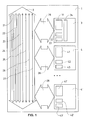
- reference number 1 refers to a device arrangement, in the electronic modules 3, 4, 4 'via bus interfaces 28 are connected to a VME bus 2.
- the device arrangement 1 comprises for example a power supply for the electrical supply of the electronic Modules 3, 4, 4 'and a housing to which the VME bus 2 is attached.
- the VME bus 2 can be used for modules 3, 4, 4 'in double Europe format as well as designed for modules 3, 4, 4 'in Europe format.
- Interrupt acknowledge signals are the electronic modules 3, 4, 4 ' using the IACKIN and IACKOUT lines, not shown separately of the VME bus 2 in a priority cascade, a so-called "Daisy chain", coupled.
- the electronic module 3 is in accordance with the standard specifications for the VME bus as VME bus master and is described in the following sections also referred to as master module 3.
- the electronic modules 4 and 4 ' are according to the standard specifications for the VME bus as VME bus slaves and are also described as slave modules in the following sections 4 and 4 '.
- the slave modules 4 and 4 comprise 4 'each a configuration slave submodule 41 or 41', the function of which in the following sections will be described in detail with reference to FIG.
- the slave modules 4 and 4 'each also include a data memory 42, respectively 42 ', preferably a data register in which the base address of the Address range is saved, the respective slave module 4, respectively 4 ', is assigned.
- the slave modules 4 and 4 'each also include one Data memory 43 or 43 ', in which module information is stored.
- the module information includes, for example, a module type or a Size of the address range required for the module in question.
- the master module 3 comprises a configuration master submodule 31, the function of which is also described in the following sections using Figure 2 is described in detail. At this point it should be pointed out that the configuration master submodule 31 is also on a slave module 4 or 4 'could be appropriate.
- the master module 3 can also a data memory 32 for storing the base address of the associated one Address area and a data memory 33 with module information include.
- CPLD Complex Programmable Logic Devices
- step S1 on the VME bus 2 the SYSRESET signal is applied on the SYSRESET line 27.
- the step S1 is in particular through the system reset control after creation an operating voltage to the device arrangement 1.
- the Step S1 can also be done by a master module 3 or by a slave module 4, 4 'are executed, for example by the configuration master submodule 31 or by another control module of a VME bus master or VME bus slaves.
- the arrows P1 and P1 ' indicate that the SYSRESET signal via the VME bus 2 to the configuration master submodule 31 and the configuration slave submodule 41 (resp 41 ') is passed, whereupon in the configuration slave submodule 41 (41'), respectively in the configuration master submodule 31, the steps S2 or S2 'are carried out become.
- step S2 the slave module 4 (4 ') is replaced by the configuration slave submodule 41 (41 ') set in a configuration mode.
- This Configuration mode are only predefined by slave module 4 (4 ') Signals on VME bus 2 observed.
- the configuration slave submodule 41 (41 ') responds only to predefined address modifier codes on the Address modifier lines 22, in particular a defined code in the user-definable Range, for example a code with the hexadecimal Value "1F". This means that the configuration slave submodule 41 only reacts to Read or write access with the predefined address modifier code "1F" can be executed.
- step S2 the configuration slave submodule sets 41 (41 ') also indicates and outputs the SYSFAIL signal on the SYSFAIL line 26 an IRQ2 signal on the IRQ2 line 25.
- the arrows P2 and P2 ' indicated that the SYSFAIL signal is applied to VME bus 2 and can be detected by the configuration master submodule 31.
- the arrows P3 and P3 ' indicate that the interrupt IRQ2 is on the VME bus 2 is created and by the configuration master submodule 31 is detected.
- step S2 ' the master module 3 is replaced by the configuration master submodule 31 in the master configuration mode and on the SYSFAIL line 26 applied the SYSFAIL signal.
- arrow P2 " indicated that the SYSFAIL signal by the configuration master submodule 31 is connected to VME bus 2.
- step S3 After detection of the IRQ2 signal checks whether the SYSFAIL signal is on VME bus 2 is created. As long as the IRQ2 signal on the VME bus 2 and the SYSFAIL signal is present, that is, as long as there is at least one Slave module 4, 4 'is in configuration mode, the configuration master submodule performs 31 configuration cycles. If on the VME bus 2 If no IRQ2 signal is applied, the master configuration mode for the Master module 3 in step S8 '.
- step S4 an IACK signal is output by the configuration master submodule 31.
- the arrows P4 and P4 ' indicate that the IACK signal on the VME bus 2 is created and by the configuration slave submodule 41 (41 ') is detected.
- Step S5 After the detection of the IACK signal in step S5, this answers Configuration slave submodule 41 (41 ') with a predefined interrupt vector, which is applied to the data lines 23. With arrows P5 and P5 ' it is indicated that the interrupt vector is applied to VME bus 2 and is detected by the configuration master submodule 31.
- step S6 the after the detection of the interrupt vector Address range, or the corresponding base address, for the slave module 4 (4 ') determined.
- the base address is determined taking into account a memory map stored in data memory 34 (a so-called "memory map") and, for example, additionally by previous Reading the module information stored in the data memory 43 (43 ').
- the dashed arrows P and P ' indicate that the Configuration master submodule 31 Module information via the VME bus 2 read from slave module 4 (4 ').
- the memory map contains the already assigned base addresses, for example a link from Base address, memory area size, module number and module type.
- the the base master is determined by the configuration master submodule 31 in the Data store 42 (42 ') written and in the memory map saved.
- the configuration master submodule 31 then sends another code, especially the hexadecimal value "55", via the VME bus 2 to the configuration slave submodule 41 (41 ') and shows this Configuration slave submodule 41 (41 ') with it, the configuration mode insurance.
- Reading module information from the data store 43 (43 ') the writing of base addresses in the data memory 42 (42') and the hexadecimal value "55” is written via the data lines 23 of the VME bus 2 using the corresponding address modifier code with the hexadecimal value "1F”.
- the arrows P6 and P6 ' indicate that the specific base address and the hexadecimal code "55" are transmitted to the slave module 4 (4 ') via the VME bus 2.
- step S7 the configuration slave submodule 41 (41 ') the SYSFAIL signal is reset (deactivated).
- the arrow P7 indicates that the configuration slave submodule 41 (41 ') receives the SYSFAIL signal resets on VME bus 2.
- step S8 the configuration mode is set by the configuration slave submodule 41 (41 ') for the slave module 4 (4') ended and that Slave module 4 (4 ') can react to standardized VME bus cycles.
- the configuration master submodule checks 31 after the execution of step S6, in step S3, whether on the SYSFAIL line 26 a SYSFAIL signal from another slave module 4 ' is created.
- step S8 ' the configuration master submodule 31 the SYSFAIL signal is reset (deactivated) and the configuration mode ended for the master module 3, after which the master module 3 normalized to VME bus cycles can respond.
- modules 3, 4, 4 'with the described configuration master submodules 31 and configuration slave submodules 41, 41 ' are in the device arrangement 1 at the same time conventional electronic modules are used, whose base addresses on the Module are defined by means of switches or "jumpers".
- the so assigned Address ranges are in the memory map mentioned above in data storage 34 saved.
Landscapes
- Engineering & Computer Science (AREA)
- Theoretical Computer Science (AREA)
- Physics & Mathematics (AREA)
- General Engineering & Computer Science (AREA)
- General Physics & Mathematics (AREA)
- Bus Control (AREA)
- Small-Scale Networks (AREA)
- Multi Processors (AREA)
Abstract
Description
Claims (10)
- Vorrichtungsanordnung (1) umfassend:dadurch gekennzeichnet, dass mindestens gewissen ersten der Module (4, 4') jeweils ein Konfigurations-Slave-Submodul (41, 41') zugeordnet ist, das so beschaffen ist, dass es, nachdem eine Betriebsspannung an die Vorrichtungsanordnung (1) angelegt wird, das betreffende erste Modul (4, 4') in einen Konfigurationsmodus setzt und in diesem Konfigurationsmodus auf vordefinierte Signale auf dem VME-Bus (2) wartet, undeinen VME-Bus (2),ein oder mehrere mit dem VME-Bus (2) verbindbare Module (3, 4, 4'), denen jeweils ein spezifischer, durch eine Basisadresse definierter Adressbereich zuweisbar ist,
dass mindestens einem zweiten der Module (3) ein Konfigurations-Master-Submodul (31) zugeordnet ist, das so beschaffen ist, dass es den ersten Modulen (4, 4'), die sich im Konfigurationsmodus befinden, jeweils eine eindeutige Basisadresse zuordnet, indem es diese Basisadresse bestimmt und in einem Datenspeicher (42, 42') des betreffenden ersten Moduls (4, 4') speichert. - Vorrichtungsanordnung (1) gemäss Anspruch 1, dadurch gekennzeichnet, dass die ersten Module (4, 4') jeweils einen Datenspeicher (43, 43') mit darin gespeicherter Modulinformation umfassen, und dass das Konfigurations-Master-Submodul (31) so beschaffen ist, dass es die gespeicherte Modulinformation liest und die Basisadresse unter Berücksichtigung der gelesenen Modulinformation bestimmt.
- Vorrichtungsanordnung (1) gemäss einem der Ansprüche 1 oder 2, dadurch gekennzeichnet, dass das Konfigurations-Slave-Submodul (41, 41') so beschaffen ist, dass es, nachdem das SYSRESET-Signal des VME-Busses (2) nach dem Anlegen der Betriebsspannung inaktiv wird, dem Konfigurations-Master-Submodul (31) den Konfigurationsmodus durch Anlegen von vordefinierten Signalen auf dem VME-Bus (2) anzeigt und dass es danach auf vordefinierte Signale auf dem VME-Bus (2) wartet.
- Vorrichtungsanordnung (1) gemäss Anspruch 3, dadurch gekennzeichnet, dass die durch das Konfigurations-Slave-Submodul (41, 41') auf dem VME-Bus (2) angelegten vordefinierten Signale das SYSFAIL-Signal und ein Interrupt-Request-Signal des VME-Busses (2) umfassen, und dass die ersten der auf dem VME-Bus (2) erwarteten vordefinierten Signale einen vordefinierten Address-Modifier-Code auf den Address-Modifier-Leitungen (22) des VME-Bus (2) umfassen.
- Vorrichtungsanordnung (1) gemäss Anspruch 4, dadurch gekennzeichnet, dass das Konfigurations-Master-Submodul (31) so beschaffen ist, dass es so lange Konfigurationszyklen durchführt wie auf dem VME-Bus (2) das Interrupt-Request-Signal und das SYSFAIL-Signal angelegt sind, wobei das Konfigurations-Master-Submodul (31) so beschaffen ist, dass es innerhalb eines Konfigurationszyklus das IACK-Signal auf dem VME-Bus (2) anlegt, einen vordefinierten Interrupt-Vektor über Datenleitungen (23) des VME-Busses (2) vom antwortenden Konfigurations-Slave-Submodul (41, 41') eines betreffenden ersten Moduls (4, 4') empfängt und die für dieses betreffende erste Modul (4, 4') bestimmte Basisadresse über die Datenleitungen (23) des VME-Busses (2) in einem Datenspeicher (42, 42') dieses betreffenden ersten Moduls (4, 4') speichert, und dass das Konfigurations-Slave-Submodul (41, 41') so beschaffen ist, dass es das SYSFAIL-Signal und den Konfigurationsmodus für das ihm zugeordnete erste Modul (4, 4') zurücksetzt, wenn eine Basisadresse in einem Datenspeicher (42, 42') des ihm zugeordneten ersten Moduls (4, 4') gespeichert wurde.
- Verfahren zum Zuordnen von Adressbereichen, die durch eine Basisadresse definiert sind, zu einem oder mehreren mit einem VME-Bus (2) verbundenen Modulen (4, 4') einer Vorrichtungsanordnung (1), dadurch gekennzeichnet, dass, nachdem eine Betriebsspannung an die Vorrichtungsanordnung (1) angelegt wird, mindestens gewisse erste der Module (4, 4') jeweils durch ein ihnen zugeordnetes Konfigurations-Slave-Submodul (41, 41') in einen Konfigurationsmodus gesetzt werden und in diesem Konfigurationsmodus auf vordefinierte Signale auf dem VME-Bus (2) warten, und
dass den ersten Modulen (4, 4'), die sich im Konfigurationsmodus befinden, durch ein mindestens einem zweiten der Module (3) zugeordnetes Konfigurations-Master-Submodul (31) jeweils eine eindeutige Basisadresse zugeordnet wird, wobei diese Basisadresse jeweils durch das Konfigurations-Master-Submodul (31) bestimmt und in einem Datenspeicher (42, 42') des betreffenden ersten Moduls (4, 4') gespeichert wird. - Verfahren gemäss Anspruch 6, dadurch gekennzeichnet, dass das Konfigurations-Master-Submodul (31) in Datenspeichern (43, 43') der ersten Module (4, 4') gespeicherte Modulinformation liest und die Basisadressen unter Berücksichtigung der gelesenen Modulinformation bestimmt.
- Verfahren gemäss einem der Ansprüche 6 oder 7, dadurch gekennzeichnet, dass die Konfigurations-Slave-Submodule (41, 41'), nachdem das SYSRESET-Signal des VME-Busses (2) nach dem Anlegen der Betriebsspannung inaktiv wird, jeweils dem Konfigurations-Master-Submodul (31) den Konfigurationsmodus durch Anlegen von vordefinierten Signalen auf dem VME-Bus (2) anzeigen und dass sie danach auf vordefinierte Signale auf dem VME-Bus (2) warten.
- Verfahren gemäss Anspruch 8, dadurch gekennzeichnet, dass die durch das Konfigurations-Slave-Submodul (41, 41') auf dem VME-Bus (2) angelegten vordefinierten Signale das SYSFAIL-Signal und ein Interrupt-Request-Signal des VME-Busses (2) umfassen, und dass die ersten der auf dem VME-Bus (2) erwarteten vordefinierten Signale einen vordefinierten Address-Modifier-Code auf den Address-Modifier-Leitungen (22) des VME-Bus (2) umfassen.
- Verfahren gemäss Anspruch 9, dadurch gekennzeichnet, dass das Konfigurations-Master-Submodul (31) so lange Konfigurationszyklen durchführt, wie auf dem VME-Bus (2) das Interrupt-Request-Signal und das SYSFAIL-Signal angelegt sind, wobei das Konfigurations-Master-Submodul (31) innerhalb eines Konfigurationszyklus das IACK-Signal auf dem VME-Bus (2) anlegt, einen vordefinierten Interrupt-Vektor über Datenleitungen (23) des VME-Busses (2) vom antwortenden Konfigurations-Slave-Submodul (41, 41') eines betreffenden ersten Moduls (4, 4') empfängt und die für dieses betreffende erste Modul (4, 4') bestimmte Basisadresse über die Datenleitungen (23) des VME-Busses (2) in einem Datenspeicher (42, 42') dieses betreffenden ersten Moduls (4, 4') speichert, und dass das Konfigurations-Slave-Submodul (41, 41') das SYSFAIL-Signal und den Konfigurationsmodus für das ihm zugeordnete erste Modul (4, 4') zurücksetzt, wenn eine Basisadresse in einem Datenspeicher (42, 42') des ihm zugeordneten ersten Moduls (4, 4') gespeichert wurde.
Priority Applications (3)
| Application Number | Priority Date | Filing Date | Title |
|---|---|---|---|
| EP02405354A EP1359511B1 (de) | 2002-04-30 | 2002-04-30 | Vorrichtungsanordung und Verfahren zur Zuordnung von Adressbereichen zu Modulen,die mit einem VME-Bus verbunden sind |
| DE50206073T DE50206073D1 (de) | 2002-04-30 | 2002-04-30 | Vorrichtungsanordung und Verfahren zur Zuordnung von Adressbereichen zu Modulen,die mit einem VME-Bus verbunden sind |
| AT02405354T ATE320630T1 (de) | 2002-04-30 | 2002-04-30 | Vorrichtungsanordung und verfahren zur zuordnung von adressbereichen zu modulen,die mit einem vme- bus verbunden sind |
Applications Claiming Priority (1)
| Application Number | Priority Date | Filing Date | Title |
|---|---|---|---|
| EP02405354A EP1359511B1 (de) | 2002-04-30 | 2002-04-30 | Vorrichtungsanordung und Verfahren zur Zuordnung von Adressbereichen zu Modulen,die mit einem VME-Bus verbunden sind |
Publications (2)
| Publication Number | Publication Date |
|---|---|
| EP1359511A1 true EP1359511A1 (de) | 2003-11-05 |
| EP1359511B1 EP1359511B1 (de) | 2006-03-15 |
Family
ID=28799768
Family Applications (1)
| Application Number | Title | Priority Date | Filing Date |
|---|---|---|---|
| EP02405354A Expired - Lifetime EP1359511B1 (de) | 2002-04-30 | 2002-04-30 | Vorrichtungsanordung und Verfahren zur Zuordnung von Adressbereichen zu Modulen,die mit einem VME-Bus verbunden sind |
Country Status (3)
| Country | Link |
|---|---|
| EP (1) | EP1359511B1 (de) |
| AT (1) | ATE320630T1 (de) |
| DE (1) | DE50206073D1 (de) |
Cited By (1)
| Publication number | Priority date | Publication date | Assignee | Title |
|---|---|---|---|---|
| CN109697179A (zh) * | 2017-10-24 | 2019-04-30 | 英业达科技有限公司 | 硬件资源扩充系统及热插入管理装置 |
Families Citing this family (1)
| Publication number | Priority date | Publication date | Assignee | Title |
|---|---|---|---|---|
| DE102020121316A1 (de) | 2020-08-13 | 2022-02-17 | Ebm-Papst Mulfingen Gmbh & Co. Kg | Einheit für ein Bussystem, Master-Slave-Bussystem mit einer Vielzahl von Einheiten und Verfahren zur Adressierung von Einheiten eines Bussystems |
Citations (2)
| Publication number | Priority date | Publication date | Assignee | Title |
|---|---|---|---|---|
| US5175536A (en) * | 1990-08-01 | 1992-12-29 | Westinghouse Electric Corp. | Apparatus and method for adapting cards designed for a VME bus for use in a VXI bus system |
| US5307475A (en) * | 1992-06-29 | 1994-04-26 | The United States Of America As Represented By The Secretary Of The Navy | Slave controller utilizing eight least/most significant bits for accessing sixteen bit data words |
-
2002
- 2002-04-30 EP EP02405354A patent/EP1359511B1/de not_active Expired - Lifetime
- 2002-04-30 AT AT02405354T patent/ATE320630T1/de not_active IP Right Cessation
- 2002-04-30 DE DE50206073T patent/DE50206073D1/de not_active Expired - Fee Related
Patent Citations (2)
| Publication number | Priority date | Publication date | Assignee | Title |
|---|---|---|---|---|
| US5175536A (en) * | 1990-08-01 | 1992-12-29 | Westinghouse Electric Corp. | Apparatus and method for adapting cards designed for a VME bus for use in a VXI bus system |
| US5307475A (en) * | 1992-06-29 | 1994-04-26 | The United States Of America As Represented By The Secretary Of The Navy | Slave controller utilizing eight least/most significant bits for accessing sixteen bit data words |
Cited By (2)
| Publication number | Priority date | Publication date | Assignee | Title |
|---|---|---|---|---|
| CN109697179A (zh) * | 2017-10-24 | 2019-04-30 | 英业达科技有限公司 | 硬件资源扩充系统及热插入管理装置 |
| CN109697179B (zh) * | 2017-10-24 | 2022-06-24 | 英业达科技有限公司 | 硬件资源扩充系统及热插入管理装置 |
Also Published As
| Publication number | Publication date |
|---|---|
| EP1359511B1 (de) | 2006-03-15 |
| DE50206073D1 (de) | 2006-05-11 |
| ATE320630T1 (de) | 2006-04-15 |
Similar Documents
| Publication | Publication Date | Title |
|---|---|---|
| DE69209538T2 (de) | Automatische Konfiguration einer Einheit für koppelbare Rechner | |
| DE3881414T2 (de) | Datenverarbeitungssystem mit einer steckbaren optionellen Karte. | |
| DE60132780T2 (de) | Mehrere ausnehmbare nichtflüchtige speicherkarten mit serieller verbindung zu einem zentralrechner | |
| DE3938018C2 (de) | ||
| DE4313190B4 (de) | Vorrichtung und Verfahren zur Initialisierung einer Datenschnittstelle für eine programmierbare Steuerung | |
| DE19614238C1 (de) | Kommunikationssystem mit einer Meisterstation und mindestens einer Sklavenstation | |
| DE19614237C1 (de) | Kommunikationssystem mit einer Meisterstation und mindestens einer Sklavenstation | |
| EP0500973B1 (de) | EEPROM und Verfahren zum Ändern einer Initialisierungsroutine im EEPROM | |
| DE102008021348A1 (de) | Halbleiterspeicher, Speicherzugriffs-Steuersystem und Datenlese-Verfahren | |
| DE3788502T2 (de) | Verfahren zur zuweisung einer leiterplattensteckplatznummer. | |
| DE60000961T2 (de) | Programmiersystem mit hoher Geschwindigkeit | |
| EP1359511B1 (de) | Vorrichtungsanordung und Verfahren zur Zuordnung von Adressbereichen zu Modulen,die mit einem VME-Bus verbunden sind | |
| DE19522335A1 (de) | Verfahren zum Einstellen von Eingabe/Ausgabe-Basisadressen und Vorrichtung für jumperfreie Konfiguration | |
| DE19525100C2 (de) | Verfahren zur On-Board-Programmierung eines elektrisch programmierbaren Nur-Lese-Speichers | |
| DE60316866T2 (de) | Verfahren und Brückenelement-Modul | |
| EP1386200B1 (de) | Verfahren und system zur lückenlosen belegung von ein- und ausgabeadressen eines modularen steuersystems | |
| EP1316891B1 (de) | Datenübertragungseinrichtung | |
| DE102022203866A1 (de) | Kommunikationssystem und Layout-Verfahren eines Kommunikationssystems | |
| EP0670062B1 (de) | Anordnung mit steckbaren funktionseinheiten | |
| DE4223398C2 (de) | Verfahren und Vorrichtung zur Programmierung von nichtflüchtigen Speichern | |
| DE4215486A1 (de) | Speichereinrichtung | |
| EP0669027B1 (de) | Anordnung zur adressierung von peripheren einheiten | |
| EP4740106A1 (de) | Anordnung für eine elektronische recheneinrichtung, sowie verfahren zum betreiben einer anordnung | |
| DE3650136T2 (de) | Schaltung zur Speicherschaltzustanderkennung. | |
| DE4121152C2 (de) | Anordnung mit einer Vielzahl von an einen Adreß-, Daten- und Steuerbus angeschlossenen Einheiten |
Legal Events
| Date | Code | Title | Description |
|---|---|---|---|
| PUAI | Public reference made under article 153(3) epc to a published international application that has entered the european phase |
Free format text: ORIGINAL CODE: 0009012 |
|
| AK | Designated contracting states |
Kind code of ref document: A1 Designated state(s): AT BE CH CY DE DK ES FI FR GB GR IE IT LI LU MC NL PT SE TR |
|
| AX | Request for extension of the european patent |
Extension state: AL LT LV MK RO SI |
|
| 17P | Request for examination filed |
Effective date: 20040116 |
|
| AKX | Designation fees paid |
Designated state(s): AT BE CH CY DE DK ES FI FR GB GR IE IT LI LU MC NL PT SE TR |
|
| GRAP | Despatch of communication of intention to grant a patent |
Free format text: ORIGINAL CODE: EPIDOSNIGR1 |
|
| GRAS | Grant fee paid |
Free format text: ORIGINAL CODE: EPIDOSNIGR3 |
|
| RAP1 | Party data changed (applicant data changed or rights of an application transferred) |
Owner name: HASLERRAIL AG |
|
| GRAA | (expected) grant |
Free format text: ORIGINAL CODE: 0009210 |
|
| AK | Designated contracting states |
Kind code of ref document: B1 Designated state(s): AT BE CH CY DE DK ES FI FR GB GR IE IT LI LU MC NL PT SE TR |
|
| PG25 | Lapsed in a contracting state [announced via postgrant information from national office to epo] |
Ref country code: IT Free format text: LAPSE BECAUSE OF FAILURE TO SUBMIT A TRANSLATION OF THE DESCRIPTION OR TO PAY THE FEE WITHIN THE PRESCRIBED TIME-LIMIT;WARNING: LAPSES OF ITALIAN PATENTS WITH EFFECTIVE DATE BEFORE 2007 MAY HAVE OCCURRED AT ANY TIME BEFORE 2007. THE CORRECT EFFECTIVE DATE MAY BE DIFFERENT FROM THE ONE RECORDED. Effective date: 20060315 Ref country code: GB Free format text: LAPSE BECAUSE OF FAILURE TO SUBMIT A TRANSLATION OF THE DESCRIPTION OR TO PAY THE FEE WITHIN THE PRESCRIBED TIME-LIMIT Effective date: 20060315 Ref country code: IE Free format text: LAPSE BECAUSE OF FAILURE TO SUBMIT A TRANSLATION OF THE DESCRIPTION OR TO PAY THE FEE WITHIN THE PRESCRIBED TIME-LIMIT Effective date: 20060315 Ref country code: NL Free format text: LAPSE BECAUSE OF FAILURE TO SUBMIT A TRANSLATION OF THE DESCRIPTION OR TO PAY THE FEE WITHIN THE PRESCRIBED TIME-LIMIT Effective date: 20060315 Ref country code: FI Free format text: LAPSE BECAUSE OF FAILURE TO SUBMIT A TRANSLATION OF THE DESCRIPTION OR TO PAY THE FEE WITHIN THE PRESCRIBED TIME-LIMIT Effective date: 20060315 |
|
| REG | Reference to a national code |
Ref country code: GB Ref legal event code: FG4D Free format text: NOT ENGLISH Ref country code: CH Ref legal event code: EP |
|
| REG | Reference to a national code |
Ref country code: IE Ref legal event code: FG4D Free format text: LANGUAGE OF EP DOCUMENT: GERMAN |
|
| REG | Reference to a national code |
Ref country code: CH Ref legal event code: NV Representative=s name: BOVARD AG PATENTANWAELTE |
|
| PG25 | Lapsed in a contracting state [announced via postgrant information from national office to epo] |
Ref country code: MC Free format text: LAPSE BECAUSE OF NON-PAYMENT OF DUE FEES Effective date: 20060430 Ref country code: BE Free format text: LAPSE BECAUSE OF NON-PAYMENT OF DUE FEES Effective date: 20060430 |
|
| PGFP | Annual fee paid to national office [announced via postgrant information from national office to epo] |
Ref country code: AT Payment date: 20060509 Year of fee payment: 5 |
|
| REF | Corresponds to: |
Ref document number: 50206073 Country of ref document: DE Date of ref document: 20060511 Kind code of ref document: P |
|
| PGFP | Annual fee paid to national office [announced via postgrant information from national office to epo] |
Ref country code: DE Payment date: 20060523 Year of fee payment: 5 |
|
| PG25 | Lapsed in a contracting state [announced via postgrant information from national office to epo] |
Ref country code: DK Free format text: LAPSE BECAUSE OF FAILURE TO SUBMIT A TRANSLATION OF THE DESCRIPTION OR TO PAY THE FEE WITHIN THE PRESCRIBED TIME-LIMIT Effective date: 20060615 Ref country code: SE Free format text: LAPSE BECAUSE OF FAILURE TO SUBMIT A TRANSLATION OF THE DESCRIPTION OR TO PAY THE FEE WITHIN THE PRESCRIBED TIME-LIMIT Effective date: 20060615 |
|
| PG25 | Lapsed in a contracting state [announced via postgrant information from national office to epo] |
Ref country code: ES Free format text: LAPSE BECAUSE OF FAILURE TO SUBMIT A TRANSLATION OF THE DESCRIPTION OR TO PAY THE FEE WITHIN THE PRESCRIBED TIME-LIMIT Effective date: 20060626 |
|
| PG25 | Lapsed in a contracting state [announced via postgrant information from national office to epo] |
Ref country code: PT Free format text: LAPSE BECAUSE OF FAILURE TO SUBMIT A TRANSLATION OF THE DESCRIPTION OR TO PAY THE FEE WITHIN THE PRESCRIBED TIME-LIMIT Effective date: 20060816 |
|
| NLV1 | Nl: lapsed or annulled due to failure to fulfill the requirements of art. 29p and 29m of the patents act | ||
| GBV | Gb: ep patent (uk) treated as always having been void in accordance with gb section 77(7)/1977 [no translation filed] |
Effective date: 20060315 |
|
| REG | Reference to a national code |
Ref country code: IE Ref legal event code: FD4D |
|
| PLBE | No opposition filed within time limit |
Free format text: ORIGINAL CODE: 0009261 |
|
| STAA | Information on the status of an ep patent application or granted ep patent |
Free format text: STATUS: NO OPPOSITION FILED WITHIN TIME LIMIT |
|
| 26N | No opposition filed |
Effective date: 20061218 |
|
| EN | Fr: translation not filed | ||
| BERE | Be: lapsed |
Owner name: HASLERRAIL A.G. Effective date: 20060430 |
|
| PG25 | Lapsed in a contracting state [announced via postgrant information from national office to epo] |
Ref country code: DE Free format text: LAPSE BECAUSE OF NON-PAYMENT OF DUE FEES Effective date: 20071101 |
|
| PG25 | Lapsed in a contracting state [announced via postgrant information from national office to epo] |
Ref country code: AT Free format text: LAPSE BECAUSE OF NON-PAYMENT OF DUE FEES Effective date: 20070430 |
|
| PG25 | Lapsed in a contracting state [announced via postgrant information from national office to epo] |
Ref country code: GR Free format text: LAPSE BECAUSE OF FAILURE TO SUBMIT A TRANSLATION OF THE DESCRIPTION OR TO PAY THE FEE WITHIN THE PRESCRIBED TIME-LIMIT Effective date: 20060616 Ref country code: FR Free format text: LAPSE BECAUSE OF FAILURE TO SUBMIT A TRANSLATION OF THE DESCRIPTION OR TO PAY THE FEE WITHIN THE PRESCRIBED TIME-LIMIT Effective date: 20070309 |
|
| PG25 | Lapsed in a contracting state [announced via postgrant information from national office to epo] |
Ref country code: LU Free format text: LAPSE BECAUSE OF NON-PAYMENT OF DUE FEES Effective date: 20060430 Ref country code: TR Free format text: LAPSE BECAUSE OF FAILURE TO SUBMIT A TRANSLATION OF THE DESCRIPTION OR TO PAY THE FEE WITHIN THE PRESCRIBED TIME-LIMIT Effective date: 20060315 |
|
| PG25 | Lapsed in a contracting state [announced via postgrant information from national office to epo] |
Ref country code: FR Free format text: LAPSE BECAUSE OF FAILURE TO SUBMIT A TRANSLATION OF THE DESCRIPTION OR TO PAY THE FEE WITHIN THE PRESCRIBED TIME-LIMIT Effective date: 20060430 |
|
| PG25 | Lapsed in a contracting state [announced via postgrant information from national office to epo] |
Ref country code: FR Free format text: LAPSE BECAUSE OF FAILURE TO SUBMIT A TRANSLATION OF THE DESCRIPTION OR TO PAY THE FEE WITHIN THE PRESCRIBED TIME-LIMIT Effective date: 20060315 Ref country code: CY Free format text: LAPSE BECAUSE OF FAILURE TO SUBMIT A TRANSLATION OF THE DESCRIPTION OR TO PAY THE FEE WITHIN THE PRESCRIBED TIME-LIMIT Effective date: 20060315 |
|
| PGFP | Annual fee paid to national office [announced via postgrant information from national office to epo] |
Ref country code: CH Payment date: 20100409 Year of fee payment: 9 |
|
| REG | Reference to a national code |
Ref country code: CH Ref legal event code: PFA Owner name: HASLERRAIL AG Free format text: HASLERRAIL AG#UNTERMATTWEG 8#3027 BERN (CH) -TRANSFER TO- HASLERRAIL AG#UNTERMATTWEG 8#3027 BERN (CH) |
|
| REG | Reference to a national code |
Ref country code: CH Ref legal event code: PL |
|
| PG25 | Lapsed in a contracting state [announced via postgrant information from national office to epo] |
Ref country code: CH Free format text: LAPSE BECAUSE OF NON-PAYMENT OF DUE FEES Effective date: 20110430 Ref country code: LI Free format text: LAPSE BECAUSE OF NON-PAYMENT OF DUE FEES Effective date: 20110430 |