EP1360882B1 - Procede de fabrication d'une couche empilable incluant un microcircuit a partir d'un microcircuit encapsule dans un boitier plastique - Google Patents
Procede de fabrication d'une couche empilable incluant un microcircuit a partir d'un microcircuit encapsule dans un boitier plastique Download PDFInfo
- Publication number
- EP1360882B1 EP1360882B1 EP02705988.0A EP02705988A EP1360882B1 EP 1360882 B1 EP1360882 B1 EP 1360882B1 EP 02705988 A EP02705988 A EP 02705988A EP 1360882 B1 EP1360882 B1 EP 1360882B1
- Authority
- EP
- European Patent Office
- Prior art keywords
- pem
- microcircuit
- modified
- die
- bond
- Prior art date
- Legal status (The legal status is an assumption and is not a legal conclusion. Google has not performed a legal analysis and makes no representation as to the accuracy of the status listed.)
- Expired - Lifetime
Links
Images




Classifications
-
- H—ELECTRICITY
- H10—SEMICONDUCTOR DEVICES; ELECTRIC SOLID-STATE DEVICES NOT OTHERWISE PROVIDED FOR
- H10W—GENERIC PACKAGES, INTERCONNECTIONS, CONNECTORS OR OTHER CONSTRUCTIONAL DETAILS OF DEVICES COVERED BY CLASS H10
- H10W74/00—Encapsulations, e.g. protective coatings
- H10W74/10—Encapsulations, e.g. protective coatings characterised by their shape or disposition
- H10W74/111—Encapsulations, e.g. protective coatings characterised by their shape or disposition the semiconductor body being completely enclosed
- H10W74/129—Encapsulations, e.g. protective coatings characterised by their shape or disposition the semiconductor body being completely enclosed forming a chip-scale package [CSP]
-
- H—ELECTRICITY
- H10—SEMICONDUCTOR DEVICES; ELECTRIC SOLID-STATE DEVICES NOT OTHERWISE PROVIDED FOR
- H10W—GENERIC PACKAGES, INTERCONNECTIONS, CONNECTORS OR OTHER CONSTRUCTIONAL DETAILS OF DEVICES COVERED BY CLASS H10
- H10W70/00—Package substrates; Interposers; Redistribution layers [RDL]
- H10W70/01—Manufacture or treatment
- H10W70/05—Manufacture or treatment of insulating or insulated package substrates, or of interposers, or of redistribution layers
- H10W70/093—Connecting or disconnecting other interconnections thereto or therefrom, e.g. connecting bond wires or bumps
-
- H—ELECTRICITY
- H10—SEMICONDUCTOR DEVICES; ELECTRIC SOLID-STATE DEVICES NOT OTHERWISE PROVIDED FOR
- H10W—GENERIC PACKAGES, INTERCONNECTIONS, CONNECTORS OR OTHER CONSTRUCTIONAL DETAILS OF DEVICES COVERED BY CLASS H10
- H10W70/00—Package substrates; Interposers; Redistribution layers [RDL]
- H10W70/60—Insulating or insulated package substrates; Interposers; Redistribution layers
-
- H—ELECTRICITY
- H10—SEMICONDUCTOR DEVICES; ELECTRIC SOLID-STATE DEVICES NOT OTHERWISE PROVIDED FOR
- H10W—GENERIC PACKAGES, INTERCONNECTIONS, CONNECTORS OR OTHER CONSTRUCTIONAL DETAILS OF DEVICES COVERED BY CLASS H10
- H10W72/00—Interconnections or connectors in packages
- H10W72/01—Manufacture or treatment
- H10W72/0198—Manufacture or treatment batch processes
-
- H—ELECTRICITY
- H10—SEMICONDUCTOR DEVICES; ELECTRIC SOLID-STATE DEVICES NOT OTHERWISE PROVIDED FOR
- H10W—GENERIC PACKAGES, INTERCONNECTIONS, CONNECTORS OR OTHER CONSTRUCTIONAL DETAILS OF DEVICES COVERED BY CLASS H10
- H10W72/00—Interconnections or connectors in packages
- H10W72/071—Connecting or disconnecting
-
- H—ELECTRICITY
- H10—SEMICONDUCTOR DEVICES; ELECTRIC SOLID-STATE DEVICES NOT OTHERWISE PROVIDED FOR
- H10W—GENERIC PACKAGES, INTERCONNECTIONS, CONNECTORS OR OTHER CONSTRUCTIONAL DETAILS OF DEVICES COVERED BY CLASS H10
- H10W72/00—Interconnections or connectors in packages
- H10W72/071—Connecting or disconnecting
- H10W72/077—Connecting of TAB connectors
-
- H—ELECTRICITY
- H10—SEMICONDUCTOR DEVICES; ELECTRIC SOLID-STATE DEVICES NOT OTHERWISE PROVIDED FOR
- H10W—GENERIC PACKAGES, INTERCONNECTIONS, CONNECTORS OR OTHER CONSTRUCTIONAL DETAILS OF DEVICES COVERED BY CLASS H10
- H10W90/00—Package configurations
-
- H—ELECTRICITY
- H10—SEMICONDUCTOR DEVICES; ELECTRIC SOLID-STATE DEVICES NOT OTHERWISE PROVIDED FOR
- H10W—GENERIC PACKAGES, INTERCONNECTIONS, CONNECTORS OR OTHER CONSTRUCTIONAL DETAILS OF DEVICES COVERED BY CLASS H10
- H10W90/00—Package configurations
- H10W90/401—Package configurations characterised by multiple insulating or insulated package substrates, interposers or RDLs
-
- H—ELECTRICITY
- H05—ELECTRIC TECHNIQUES NOT OTHERWISE PROVIDED FOR
- H05K—PRINTED CIRCUITS; CASINGS OR CONSTRUCTIONAL DETAILS OF ELECTRIC APPARATUS; MANUFACTURE OF ASSEMBLAGES OF ELECTRICAL COMPONENTS
- H05K1/00—Printed circuits
- H05K1/02—Details
- H05K1/14—Structural association of two or more printed circuits
- H05K1/144—Stacked arrangements of planar printed circuit boards
-
- H—ELECTRICITY
- H10—SEMICONDUCTOR DEVICES; ELECTRIC SOLID-STATE DEVICES NOT OTHERWISE PROVIDED FOR
- H10W—GENERIC PACKAGES, INTERCONNECTIONS, CONNECTORS OR OTHER CONSTRUCTIONAL DETAILS OF DEVICES COVERED BY CLASS H10
- H10W72/00—Interconnections or connectors in packages
- H10W72/071—Connecting or disconnecting
- H10W72/072—Connecting or disconnecting of bump connectors
-
- H—ELECTRICITY
- H10—SEMICONDUCTOR DEVICES; ELECTRIC SOLID-STATE DEVICES NOT OTHERWISE PROVIDED FOR
- H10W—GENERIC PACKAGES, INTERCONNECTIONS, CONNECTORS OR OTHER CONSTRUCTIONAL DETAILS OF DEVICES COVERED BY CLASS H10
- H10W72/00—Interconnections or connectors in packages
- H10W72/071—Connecting or disconnecting
- H10W72/072—Connecting or disconnecting of bump connectors
- H10W72/07231—Techniques
- H10W72/07236—Soldering or alloying
-
- H—ELECTRICITY
- H10—SEMICONDUCTOR DEVICES; ELECTRIC SOLID-STATE DEVICES NOT OTHERWISE PROVIDED FOR
- H10W—GENERIC PACKAGES, INTERCONNECTIONS, CONNECTORS OR OTHER CONSTRUCTIONAL DETAILS OF DEVICES COVERED BY CLASS H10
- H10W72/00—Interconnections or connectors in packages
- H10W72/071—Connecting or disconnecting
- H10W72/073—Connecting or disconnecting of die-attach connectors
- H10W72/07351—Connecting or disconnecting of die-attach connectors characterised by changes in properties of the die-attach connectors during connecting
- H10W72/07352—Connecting or disconnecting of die-attach connectors characterised by changes in properties of the die-attach connectors during connecting changes in structures or sizes
-
- H—ELECTRICITY
- H10—SEMICONDUCTOR DEVICES; ELECTRIC SOLID-STATE DEVICES NOT OTHERWISE PROVIDED FOR
- H10W—GENERIC PACKAGES, INTERCONNECTIONS, CONNECTORS OR OTHER CONSTRUCTIONAL DETAILS OF DEVICES COVERED BY CLASS H10
- H10W72/00—Interconnections or connectors in packages
- H10W72/071—Connecting or disconnecting
- H10W72/075—Connecting or disconnecting of bond wires
- H10W72/07531—Techniques
- H10W72/07532—Compression bonding, e.g. thermocompression bonding
- H10W72/07533—Ultrasonic bonding, e.g. thermosonic bonding
-
- H—ELECTRICITY
- H10—SEMICONDUCTOR DEVICES; ELECTRIC SOLID-STATE DEVICES NOT OTHERWISE PROVIDED FOR
- H10W—GENERIC PACKAGES, INTERCONNECTIONS, CONNECTORS OR OTHER CONSTRUCTIONAL DETAILS OF DEVICES COVERED BY CLASS H10
- H10W72/00—Interconnections or connectors in packages
- H10W72/30—Die-attach connectors
-
- H—ELECTRICITY
- H10—SEMICONDUCTOR DEVICES; ELECTRIC SOLID-STATE DEVICES NOT OTHERWISE PROVIDED FOR
- H10W—GENERIC PACKAGES, INTERCONNECTIONS, CONNECTORS OR OTHER CONSTRUCTIONAL DETAILS OF DEVICES COVERED BY CLASS H10
- H10W72/00—Interconnections or connectors in packages
- H10W72/30—Die-attach connectors
- H10W72/321—Structures or relative sizes of die-attach connectors
-
- H—ELECTRICITY
- H10—SEMICONDUCTOR DEVICES; ELECTRIC SOLID-STATE DEVICES NOT OTHERWISE PROVIDED FOR
- H10W—GENERIC PACKAGES, INTERCONNECTIONS, CONNECTORS OR OTHER CONSTRUCTIONAL DETAILS OF DEVICES COVERED BY CLASS H10
- H10W72/00—Interconnections or connectors in packages
- H10W72/50—Bond wires
- H10W72/531—Shapes of wire connectors
- H10W72/536—Shapes of wire connectors the connected ends being ball-shaped
-
- H—ELECTRICITY
- H10—SEMICONDUCTOR DEVICES; ELECTRIC SOLID-STATE DEVICES NOT OTHERWISE PROVIDED FOR
- H10W—GENERIC PACKAGES, INTERCONNECTIONS, CONNECTORS OR OTHER CONSTRUCTIONAL DETAILS OF DEVICES COVERED BY CLASS H10
- H10W72/00—Interconnections or connectors in packages
- H10W72/50—Bond wires
- H10W72/531—Shapes of wire connectors
- H10W72/5363—Shapes of wire connectors the connected ends being wedge-shaped
-
- H—ELECTRICITY
- H10—SEMICONDUCTOR DEVICES; ELECTRIC SOLID-STATE DEVICES NOT OTHERWISE PROVIDED FOR
- H10W—GENERIC PACKAGES, INTERCONNECTIONS, CONNECTORS OR OTHER CONSTRUCTIONAL DETAILS OF DEVICES COVERED BY CLASS H10
- H10W72/00—Interconnections or connectors in packages
- H10W72/50—Bond wires
- H10W72/551—Materials of bond wires
- H10W72/552—Materials of bond wires comprising metals or metalloids, e.g. silver
- H10W72/5522—Materials of bond wires comprising metals or metalloids, e.g. silver comprising gold [Au]
-
- H—ELECTRICITY
- H10—SEMICONDUCTOR DEVICES; ELECTRIC SOLID-STATE DEVICES NOT OTHERWISE PROVIDED FOR
- H10W—GENERIC PACKAGES, INTERCONNECTIONS, CONNECTORS OR OTHER CONSTRUCTIONAL DETAILS OF DEVICES COVERED BY CLASS H10
- H10W72/00—Interconnections or connectors in packages
- H10W72/701—Tape-automated bond [TAB] connectors
-
- H—ELECTRICITY
- H10—SEMICONDUCTOR DEVICES; ELECTRIC SOLID-STATE DEVICES NOT OTHERWISE PROVIDED FOR
- H10W—GENERIC PACKAGES, INTERCONNECTIONS, CONNECTORS OR OTHER CONSTRUCTIONAL DETAILS OF DEVICES COVERED BY CLASS H10
- H10W72/00—Interconnections or connectors in packages
- H10W72/801—Interconnections on sidewalls of containers
-
- H—ELECTRICITY
- H10—SEMICONDUCTOR DEVICES; ELECTRIC SOLID-STATE DEVICES NOT OTHERWISE PROVIDED FOR
- H10W—GENERIC PACKAGES, INTERCONNECTIONS, CONNECTORS OR OTHER CONSTRUCTIONAL DETAILS OF DEVICES COVERED BY CLASS H10
- H10W72/00—Interconnections or connectors in packages
- H10W72/851—Dispositions of multiple connectors or interconnections
- H10W72/874—On different surfaces
-
- H—ELECTRICITY
- H10—SEMICONDUCTOR DEVICES; ELECTRIC SOLID-STATE DEVICES NOT OTHERWISE PROVIDED FOR
- H10W—GENERIC PACKAGES, INTERCONNECTIONS, CONNECTORS OR OTHER CONSTRUCTIONAL DETAILS OF DEVICES COVERED BY CLASS H10
- H10W72/00—Interconnections or connectors in packages
- H10W72/90—Bond pads, in general
- H10W72/941—Dispositions of bond pads
- H10W72/9413—Dispositions of bond pads on encapsulations
-
- H—ELECTRICITY
- H10—SEMICONDUCTOR DEVICES; ELECTRIC SOLID-STATE DEVICES NOT OTHERWISE PROVIDED FOR
- H10W—GENERIC PACKAGES, INTERCONNECTIONS, CONNECTORS OR OTHER CONSTRUCTIONAL DETAILS OF DEVICES COVERED BY CLASS H10
- H10W74/00—Encapsulations, e.g. protective coatings
-
- H—ELECTRICITY
- H10—SEMICONDUCTOR DEVICES; ELECTRIC SOLID-STATE DEVICES NOT OTHERWISE PROVIDED FOR
- H10W—GENERIC PACKAGES, INTERCONNECTIONS, CONNECTORS OR OTHER CONSTRUCTIONAL DETAILS OF DEVICES COVERED BY CLASS H10
- H10W74/00—Encapsulations, e.g. protective coatings
- H10W74/10—Encapsulations, e.g. protective coatings characterised by their shape or disposition
- H10W74/131—Encapsulations, e.g. protective coatings characterised by their shape or disposition the semiconductor body being only partially enclosed
- H10W74/142—Encapsulations, e.g. protective coatings characterised by their shape or disposition the semiconductor body being only partially enclosed the encapsulations exposing the passive side of the semiconductor body
-
- H—ELECTRICITY
- H10—SEMICONDUCTOR DEVICES; ELECTRIC SOLID-STATE DEVICES NOT OTHERWISE PROVIDED FOR
- H10W—GENERIC PACKAGES, INTERCONNECTIONS, CONNECTORS OR OTHER CONSTRUCTIONAL DETAILS OF DEVICES COVERED BY CLASS H10
- H10W90/00—Package configurations
- H10W90/701—Package configurations characterised by the relative positions of pads or connectors relative to package parts
- H10W90/751—Package configurations characterised by the relative positions of pads or connectors relative to package parts of bond wires
- H10W90/756—Package configurations characterised by the relative positions of pads or connectors relative to package parts of bond wires between a chip and a stacked lead frame, conducting package substrate or heat sink
-
- Y—GENERAL TAGGING OF NEW TECHNOLOGICAL DEVELOPMENTS; GENERAL TAGGING OF CROSS-SECTIONAL TECHNOLOGIES SPANNING OVER SEVERAL SECTIONS OF THE IPC; TECHNICAL SUBJECTS COVERED BY FORMER USPC CROSS-REFERENCE ART COLLECTIONS [XRACs] AND DIGESTS
- Y10—TECHNICAL SUBJECTS COVERED BY FORMER USPC
- Y10T—TECHNICAL SUBJECTS COVERED BY FORMER US CLASSIFICATION
- Y10T29/00—Metal working
- Y10T29/49—Method of mechanical manufacture
- Y10T29/49002—Electrical device making
- Y10T29/49117—Conductor or circuit manufacturing
- Y10T29/49124—On flat or curved insulated base, e.g., printed circuit, etc.
- Y10T29/49126—Assembling bases
-
- Y—GENERAL TAGGING OF NEW TECHNOLOGICAL DEVELOPMENTS; GENERAL TAGGING OF CROSS-SECTIONAL TECHNOLOGIES SPANNING OVER SEVERAL SECTIONS OF THE IPC; TECHNICAL SUBJECTS COVERED BY FORMER USPC CROSS-REFERENCE ART COLLECTIONS [XRACs] AND DIGESTS
- Y10—TECHNICAL SUBJECTS COVERED BY FORMER USPC
- Y10T—TECHNICAL SUBJECTS COVERED BY FORMER US CLASSIFICATION
- Y10T29/00—Metal working
- Y10T29/49—Method of mechanical manufacture
- Y10T29/49002—Electrical device making
- Y10T29/49117—Conductor or circuit manufacturing
- Y10T29/49124—On flat or curved insulated base, e.g., printed circuit, etc.
- Y10T29/4913—Assembling to base an electrical component, e.g., capacitor, etc.
- Y10T29/49144—Assembling to base an electrical component, e.g., capacitor, etc. by metal fusion
-
- Y—GENERAL TAGGING OF NEW TECHNOLOGICAL DEVELOPMENTS; GENERAL TAGGING OF CROSS-SECTIONAL TECHNOLOGIES SPANNING OVER SEVERAL SECTIONS OF THE IPC; TECHNICAL SUBJECTS COVERED BY FORMER USPC CROSS-REFERENCE ART COLLECTIONS [XRACs] AND DIGESTS
- Y10—TECHNICAL SUBJECTS COVERED BY FORMER USPC
- Y10T—TECHNICAL SUBJECTS COVERED BY FORMER US CLASSIFICATION
- Y10T29/00—Metal working
- Y10T29/49—Method of mechanical manufacture
- Y10T29/49002—Electrical device making
- Y10T29/49117—Conductor or circuit manufacturing
- Y10T29/49124—On flat or curved insulated base, e.g., printed circuit, etc.
- Y10T29/4913—Assembling to base an electrical component, e.g., capacitor, etc.
- Y10T29/49146—Assembling to base an electrical component, e.g., capacitor, etc. with encapsulating, e.g., potting, etc.
Definitions
- This invention relates generally to the dense packaging of electronic circuitry through the stacking of integrated circuit (IC) chips (aka microcircuits or die) and, more specifically, to a method of making a stackable microcircuit layer starting from a plastic encapsulated microcircuit.
- IC integrated circuit
- Irvine Sensors Corporation has been a leader in developing high density packaging of IC chips, originally for use in focal plane modules, and then for use in a variety of computer functions, such as memory.
- Irvine Sensors is listed as a developer of "bare die assemblies" using "custom ICs”.
- stacking of IC chips has emphasized use of identical-area chips, each of which performs the same function.
- the resulting stack is a rectangular parallelepiped (or cube) having substantially planar outer surfaces.
- One or more of the outer surfaces is an access plane, reached by electrical leads from the IC circuitry of the stacked chips, in order to permit connection to external circuitry.
- Irvine Sensors was initially "stacking silicon" by (1) buying whole silicon wafers from a wafer manufacturer, (2) metalizing an upper surface of the wafer to connect each die's bond pads to an edge that will later be formed when the die is diced from the wafer; (3) dicing stackable die from the metallized wafer; (4) stacking the stackable die to form die-stacks, and then (5) forming edge connections on one or more sides of each die stack.
- Irvine Sensors found it troublesome to make die stacks by stacking silicon die, however, for several reason.
- the edge connects on the die stacks because they must be made within the dicing streets that have grown continually narrower as dicing technologies have improved.
- a die's original metallization may be undesirably exposed to the edge and thereby make it troublesome to form further access plane metallization along that edge without shorting.
- Irvine Sensors has two patents that relate to "Neo-Wafers" and "Neo-Chips", i.e. U.S. Patent No. 5,953,588 entitled “STACKABLE LAYERS CONTAINING ENCAPSULATED IC CHIPS” and U.S. Patent No. 6,072,234 entitled “STACK OF EQUAL LAYER NEO-CHIPS CONTAINING ENCAPSULATED IC CHIPS OF DIFFERENT SIZES.”
- Neo-Wafer As disclosed more fully in the foregoing patents, the inventors make a "Neo-Wafer” by (1) buying bare die (preferably pre-tested or "known good” die); (2) arranging the bare die in a spaced arrangement within a wafer- shaped fixture; and then (3) pouring a potting material such as epoxy onto the bare die within the wafer-shaped fixture.
- the Neo-Wafers after being removed from the fixture, are surface metalized and the potted die are cut from the Neo-Wafers to provide "Neo-Chips" of equal area that are suitable for stacking.
- a significant benefit of Neo-Wafer and Neo-Chips is that know good die may be used and different sized and number of die may be incorporated into same sized Neo-Chips.
- Neo-stacking offers significant improvements over silicon die stacking, but it also proved troublesome under certain market circumstances. In particular, it is often difficult to buy bare die because many manufacturers will only sell only packaged die.
- US 5424254 discloses a method of recovering bare semiconductor chips from plastic packaged modules by thermal shock. The method includes in particular the steps of: a) polishing the module topside to eliminate the top part of the plastic encapsulating resin until the conductors of the lead frame are exposed and b) removing the lead frame. There remains a need, therefore, for a method of making a stackable microcircuit layer starting from a plastic encapsulated microcircuit.
- the present invention is directed to a method of modifying a plastic encapsulated microcircuit (PEM) to make a stackable microcircuit layer according to claim 1.
- PEM plastic encapsulated microcircuit
- bare die have been potted in special fixtures in order to create stackable microcircuit layers known as "neo-chips".
- bare die are not always available and even when they are, the manufacture's testing is often limited to statistical "pass/fail” verifications using parametric measurements and suitable guard bands.
- the present invention is directed to creating stackable microcircuit layers in a novel "reverse” manner, i.e. by starting with plastic encapsulated microcircuits (PEMs) or, in other words, by starting with already packaged die.
- PEMs plastic encapsulated microcircuits
- PEMs are readily available for purchase in the marketplace.
- the die contained in the PEMs are usually pre-tested and fully burned-in by the manufacturer.
- Figure 1 shows, by way of background, a die 210 that includes an active surface 211 containing integrated circuitry and a plurality of bond pads 212.
- wires are bonded to the bond pads 212 in order to provide power, communicate control signals, and the like, to and from the circuitry via the leads of a package that suitably contains the die 210.
- the bond pads 212 are arranged in a straight line down the center of the die 210, but the actual arrangement of bond pads may vary. Dies like that shown in Figure 1 are carried in all varieties of packages, two of which are discussed below.
- FIG. 2 shows a typical plastic encapsulated microcircuit (PEM) 300 that is formed from a plastic, injection molded encapsulant 310 and may be used to practice this invention.
- the particular PEM 300 of Figure 2 is a 54-pin TSOP (Thin Small Outline Package) that has a plurality of leads 272 extending from the encapsulant 310.
- TSOP Thin Small Outline Package
- Figure 3 shows that the die 210 is encapsulated inside of the PEM 300.
- the die's bond pads 212 are electrically connected to a lead frame 270 that is encapsulated along with the die 210 while providing the leads 272 that extend from the PEM's encapsulant 310.
- Figures 4a to 4f are cross-sectional views that illustrate the steps of a preferred method of modifying the PEM 300 of Figure 3 to first form a modified PEM 400 and ultimately to form a stackable microcircuit layer 400*.
- a first embodiment of the herein disclosed method of making a stackable microcircuit layer 400* comprising the steps of: providing a PEM 300 that includes (a) a microcircuit 210 having an active surface 211 containing integrated circuitry and a bond pad 212, and (b) an encapsulant 310 in contact with the microcircuit 210; and modifying the PEM 300 to produce a modified PEM 400 having a modified surface on which modified surface is exposed a conductive member (e.g. a section of the ball bond 231 or a section of the wire 232) that is electrically connected to the bond pad 212.
- a conductive member e.g. a section of the ball bond 231 or a section of the wire 232
- FIG 4a is a cross-sectional view of the PEM 300 of Figure 3 , taken along section lines 4-4, showing the internal die 210 and a conductive lead assembly 230 contained inside of the encapsulant 310.
- the conductive lead assembly 230 in this particular PEM 300 was formed by using a lead frame adhesive 320 (typically, in the case of a TSOP, a polymide adhesive layer that is located on either side of the bond pads 212) to secure a lead frame 270 above the die 210.
- a thermosonic ball bond process was used to connect the bond pads 212 to the lead frame 270.
- a plurality of wires 232 are connected from each bond pad 212 to a corresponding portion of the lead frame 270 by first forming a gold ball 231 at one end of the wire 232, ultrasonically bonding the gold ball 231 to the bond pad 212, and then compressing the other end of the wire 212 to the lead frame 270 to form a so-called "crescent bond" on the lead frame.
- the PEM's encapsulant 310 usually formed in an injection molding process, surrounds the die 210 and includes an upper portion 311 that covers the conductive lead assembly 230 (gold ball 231, wire 232, and lead frame 270).
- Figure 4b relates to modifying the PEM 300, here by grinding or top thinning. Other alternatives could be used, of course, such as wet etching, dry etching as with a plasma, hand lapping with a diamond paste, and so on.
- Figure 4b shows a first preferred method of modifying the PEM 300 to form a modified PEM 400.
- the PEM 300 is ground from the top through the lead frame 270
- this modifying step is accomplished by grinding a topside of the PEM 300 of Figure 4a in order to remove the lead frame 270, in order to expose an upper surface of the lead frame adhesive 320 that once secured the lead frame 270, and in order to expose a conductive member that is electrically connected to the bond pad 212 (e.g. a section of the wire 232 and/or a section of the gold ball bond 231).
- the presently preferred method of grinding involves using a Strausbaugh wafer grinder with the PEM mounted on a blank dummy wafer, but different grinding methods may be used.
- Figure 4c relates to adding reroute metal by forming an electrical lead 241 on the modified surface of the modified PEM 400.
- Figure 4c shows the modified PEM 400 after application of metallization 241 that connects the die's bond pad 212, via the gold ball bond 231, with an edge 411 of the modified PEM 400.
- the processes used to lay down the reroute metaliization are well known.
- One such process involves sputtering on a field layer of metal, applying an emulsion and processing it to define the desired pattern; and then etching away the undesired portions of the field layer to leave only the desired metallization.
- the reroute metallization may be applied to each modified PEM 400, one at a time, or to several at a time by establishing a suitable gang processing procedure. It should be noted that in some applications it may be possible to retain the original lead frame 270 and not apply new reroute metal 24. This is particularly true for memory stacking applications where the access plane connections on the side of the stack are highly bused.
- Figure 4d relates to adding an insulating layer 250 that covers the electrical reroute lead 241.
- Figure 4d shows the modified PEM 400 after application of an insulating layer 250.
- the preferred insulating layer 250 is a polyimide that is spun on or sprayed on as desired.
- Figure 4e relates to an optional back thinning step.
- Figure 4e shows the modified PEM 400 after such backside thinning.
- Backside thinning is particular desirable in the case of a TSOP because it makes the ultimate stackable microcircuit layer 400* thinner (about 10 mils in thickness), because it removes plastic that would otherwise be thermally insulative, and because it allow for tighter height tolerance that may prevent tolerance runout when connecting to separate electrically isolated leads in a stack of the microcircuit layers 400*.
- Figure 4f relates to an optionally reducing the area of the modified PEM 500 by, in this case, dicing.
- Figure 4f shows the final stackable microcircuit layer 400* that is formed by dicing the modified PEM 400 of Figure 4e along the dashed lines.
- the stackable microcircuit layer 400* is comparable to a Neo-Chip except that here the die 210 was provided as part of a PEM 300 and was likely burned-in by the manufacturer and here the die 210 is surrounded by a portion of the encapsulant 310 that was part of the original PEM 300 rather than by an after-added potting material such as epoxy.
- Figure 5 shows a typical stack 450 that may be formed from several stackable microcircuit layers 400*, including a cap chip 451 that provides interface pads that are electrically connected to metallization 453 that is formed along an access plane of the stack 450 in order to provide so- called "t-connections" with the reroute metallization 241 (or original lead frames) of the individual layers 400*.
- the preferred cap chip 451 is a printed circuit board, but it could be made from any suitable insulator (e.g. ceramic) that can be processed to provide the required via holes (not separately numbered).
- the stack is homogenous, but it is also possible, of course, to produce stacks of equal or unequal area layers that contain different sized and differently numbers of die.
- a stackable microcircuit layer 400* may itself be further potted, alone or with other die, to create a neo-chip of greater area or enhanced capability.
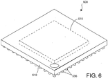
- Figure 6 is a perspective view of a plastic encapsulated microcircuit 600 provided as a micro-Ball Grid Array ( ⁇ BGA) package that is formed from an encapsulant 610 that contains a die 510 (dashed lines) that is electrically connected (not shown) to a plurality of solder ball terminals 536 arranged in a grid pattern on a bottom side of the package.
- ⁇ BGA micro-Ball Grid Array
- FIG. 7a A method of modifying PEM 600 in the form of a ⁇ BGA Package is illustrated by Figures Figures 7a to 7d .
- Figure 7a is our starting place in that it shows an inverted, cross- sectional view of the PEM 600 of Figure 6 (simplified to show only two solder ball terminals 536).
- Figure 7a shows that the die 510 and the conductive lead assembly 530 are contained inside of the encapsulant 610. There are some important differences, however, relative to the TSOP PEM 300.
- the ⁇ BGA PEM 600 includes a flexible lead beam 531 that is supported on an elastomeric pad 620 having one end adhered to the bond pad 512 and another end in contact with a deposited solder ball 536.
- the flexible lead beam 531 is typically formed from a conductive trace provided on a flexible substrate such as a polyimide film.
- a succession of insulating layers 631 are provided in the original manufacture of the PEM 600.
- Figure 7b like Figure 4b , relates to modifying the PEM.
- the modifying is not accomplished by grinding or top thinning, but rather by removing at least a portion of the solder balls 536.
- the removing of at least a portion of the solder ball is accomplished by heating the solder ball to form molten solder and wicking away the molten solder. It may also be possible to remove a portion of the solder balls 536 through a mechanical shearing operation.
- Figure 7b shows a modified PEM 700 formed by removing the solder balls 536 such that one end 534 of a flexible lead beam 531 is exposed;
- Figure 7c like Figure 4c , relates to adding reroute metal by forming an electrical lead 541 on the modified surface of the modified PEM 700.
- Figure 7c shows the modified PEM 700 after application of reroute metallization 541 that connects the die's bond pad 512, via the flexible lead beam 531 that has one end 533 in contact with the bond pad 512 and another end 534 exposed to the metallization 543, with an edge 711 of the modified PEM 700;
- Figure 7d like Figure 4d , relates to adding an insulating layer 550 that covers the electrical reroute lead 541. At this point, the result is the final stackable microcircuit layer 700*. There is no need for back thinning or reduction in area as in Figures 4e and 4f above because the uBGA was thin and chip scale to begin.
- Figure 8 shows a typical stack 750 that may be formed from several stackable microcircuit layers 700*, including a cap chip 751 that provides interface pads that are electrically connected to metallization 753 that is formed along an access plane of the stack 750 in order to provide so- called "t-connections" with the reroute metallization 541 of the individual layers 700*.
- Figure 8 is comparable to Figure 5 .
- the stack 750 is shows as homogenous, but it is also possible, of course, to produce a stack of equal or unequal area layers that contain different sized and differently numbers of die. It should also be noted that a stackable microcircuit layer 700* may itself be further potted, alone or with other die, to create a neo-chip of greater area or enhanced capability.
Landscapes
- Structures Or Materials For Encapsulating Or Coating Semiconductor Devices Or Solid State Devices (AREA)
- Encapsulation Of And Coatings For Semiconductor Or Solid State Devices (AREA)
Claims (15)
- Procédé de modification d'un microcircuit encapsulé en plastique (PEM) pour fabriquer une couche de microcircuits empilables comprenant les étapes consistant à :(i) fournir un PEM (300) qui comprend (a) un microcircuit (210) présentant une surface active contenant des circuits intégrés et des plots de soudure (212) (b) des éléments conducteurs (231), ce qui permet à chaque plot de soudure d'être soudé et connecté électriquement à un élément conducteur et (c) l'agent d'encapsulation (310) étant un corps en plastique en contact avec le microcircuit, dans lequel le microcircuit et les éléments conducteurs sont encapsulés à l'intérieur de l'agent d'encapsulation et dans lequel le PEM comprend les conducteurs d'une grille de connexion (270) qui sont connectés électriquement aux éléments conducteurs, ladite grille de connexion étant partiellement encapsulée à l'intérieur de l'agent d'encapsulation et lesdits conducteurs s'étendant hors de l'agent d'encapsulation ;(ii) modifier le PEM pour produire un PEM modifié (400) présentant une surface modifiée par amincissement à partir d'un premier côté du PEM pour supprimer les conducteurs et exposer les éléments conducteurs ; et(iii) former un conducteur électrique (241) sur la surface modifiée du PEM modifié qui conduit à partir d'un élément conducteur à un bord du PEM modifié.
- Procédé selon la revendication 1, dans lequel le microcircuit est un microcircuit prétesté.
- Procédé selon la revendication 1, dans lequel le microcircuit est un microcircuit fiabilisé.
- Procédé selon la revendication 1, dans lequel la modification de l'étape est réalisée par meulage.
- Procédé selon la revendication 1 comprenant en outre l'étape de recouvrement du conducteur électrique avec une couche isolante.
- Procédé selon la revendication 1 comprenant l'étape supplémentaire de réduction de l'épaisseur du PEM modifié par amincissement de la face arrière du PEM modifié qui est en regard de l'élément conducteur.
- Procédé selon la revendication 6, dans lequel l'étape de réduction de l'épaisseur du PEM modifié par amincissement de la face arrière du PEM modifié est réalisé par meulage.
- Procédé selon la revendication 1 comprenant l'étape supplémentaire de réduction de la surface du PEM modifié.
- Procédé selon la revendication 8, dans lequel l'étape supplémentaire de réduction de la surface du PEM modifié est accomplie par le sciage du PEM modifié le long d'un ou plusieurs bords.
- Procédé selon la revendication 1, dans lequel les éléments conducteurs qui connectent électriquement aux plots de soudure sont chacun une partie d'une soudure par fil.
- Procédé selon la revendication 10 dans lequel l'élément conducteur est une soudure par boule d'or.
- Procédé selon la revendication 10 dans lequel l'élément conducteur est un fil.
- Procédé selon la revendication 10 dans lequel l'élément conducteur est une soudure en coin.
- Le procédé selon la revendication 1, dans lequel le PEM comprend un boîtier mince à connexions courtes (TSOP) contenant des soudures par boule d'or, des conducteurs d'une grille de connexion et des fils qui sont collectivement encapsulés dans le corps en plastique du PEM, dans laquelle une soudure par boule d'or est formée sur chaque plot de soudure, dans lequel chaque fil connecte une soudure par boule d'or à un conducteur et dans lequel les soudures par boule d'or sont les éléments conducteurs apparents sur la surface modifiée du PEM modifié par amincissement.
- Procédé selon la revendication 14, dans lequel l'amincissement supprime la grille de connexion et les fils en même temps qu'une portion du corps en plastique
Applications Claiming Priority (3)
| Application Number | Priority Date | Filing Date | Title |
|---|---|---|---|
| US770864 | 2001-01-26 | ||
| US09/770,864 US20020100600A1 (en) | 2001-01-26 | 2001-01-26 | Stackable microcircuit layer formed from a plastic encapsulated microcircuit and method of making the same |
| PCT/US2002/002276 WO2002062118A1 (fr) | 2001-01-26 | 2002-01-25 | Couche a microcircuit empilable constituee d'un microcircuit a encapsulation plastique et son procede de fabrication |
Publications (3)
| Publication Number | Publication Date |
|---|---|
| EP1360882A1 EP1360882A1 (fr) | 2003-11-12 |
| EP1360882A4 EP1360882A4 (fr) | 2009-05-06 |
| EP1360882B1 true EP1360882B1 (fr) | 2018-06-13 |
Family
ID=25089941
Family Applications (1)
| Application Number | Title | Priority Date | Filing Date |
|---|---|---|---|
| EP02705988.0A Expired - Lifetime EP1360882B1 (fr) | 2001-01-26 | 2002-01-25 | Procede de fabrication d'une couche empilable incluant un microcircuit a partir d'un microcircuit encapsule dans un boitier plastique |
Country Status (4)
| Country | Link |
|---|---|
| US (2) | US20020100600A1 (fr) |
| EP (1) | EP1360882B1 (fr) |
| JP (1) | JP2004523902A (fr) |
| WO (1) | WO2002062118A1 (fr) |
Families Citing this family (56)
| Publication number | Priority date | Publication date | Assignee | Title |
|---|---|---|---|---|
| US7174627B2 (en) * | 2001-01-26 | 2007-02-13 | Irvine Sensors Corporation | Method of fabricating known good dies from packaged integrated circuits |
| US20030221313A1 (en) * | 2001-01-26 | 2003-12-04 | Gann Keith D. | Method for making stacked integrated circuits (ICs) using prepackaged parts |
| DE10231385B4 (de) * | 2001-07-10 | 2007-02-22 | Samsung Electronics Co., Ltd., Suwon | Halbleiterchip mit Bondkontaktstellen und zugehörige Mehrchippackung |
| US6667225B2 (en) * | 2001-12-17 | 2003-12-23 | Intel Corporation | Wafer-bonding using solder and method of making the same |
| US6690088B2 (en) * | 2002-01-31 | 2004-02-10 | Macintyre Donald M. | Integrated circuit package stacking structure |
| US6806559B2 (en) | 2002-04-22 | 2004-10-19 | Irvine Sensors Corporation | Method and apparatus for connecting vertically stacked integrated circuit chips |
| US7777321B2 (en) | 2002-04-22 | 2010-08-17 | Gann Keith D | Stacked microelectronic layer and module with three-axis channel T-connects |
| CN1672475B (zh) * | 2002-06-27 | 2011-11-23 | Ppg工业俄亥俄公司 | 有凹入或伸长分离接头片的单层或多层印刷电路板及其制造方法 |
| KR100621991B1 (ko) * | 2003-01-03 | 2006-09-13 | 삼성전자주식회사 | 칩 스케일 적층 패키지 |
| US20040264148A1 (en) * | 2003-06-27 | 2004-12-30 | Burdick William Edward | Method and system for fan fold packaging |
| US7214605B2 (en) * | 2003-10-09 | 2007-05-08 | Intel Corporation | Deposition of diffusion barrier |
| US8074082B2 (en) * | 2004-10-08 | 2011-12-06 | Aprolase Development Co., Llc | Anti-tamper module |
| DE102004057485B4 (de) * | 2004-11-29 | 2007-10-18 | Infineon Technologies Ag | Leistungshalbleiterbauelement und Verfahren zu dessen Herstellung |
| US7709943B2 (en) | 2005-02-14 | 2010-05-04 | Daniel Michaels | Stacked ball grid array package module utilizing one or more interposer layers |
| EP1724835A1 (fr) * | 2005-05-17 | 2006-11-22 | Irvine Sensors Corporation | Composant électronique, comprenant une couche avec un circuit intégré et procédé de fabrication |
| JP4819398B2 (ja) * | 2005-05-18 | 2011-11-24 | アプロレーザ ディベロップメント カンパニー リミテッド ライアビリティー カンパニー | 電子モジュール |
| US8051557B2 (en) * | 2006-03-31 | 2011-11-08 | Princo Corp. | Substrate with multi-layer interconnection structure and method of manufacturing the same |
| US7990727B1 (en) | 2006-04-03 | 2011-08-02 | Aprolase Development Co., Llc | Ball grid array stack |
| US7901989B2 (en) * | 2006-10-10 | 2011-03-08 | Tessera, Inc. | Reconstituted wafer level stacking |
| US8723332B2 (en) | 2007-06-11 | 2014-05-13 | Invensas Corporation | Electrically interconnected stacked die assemblies |
| US7923349B2 (en) * | 2007-06-19 | 2011-04-12 | Vertical Circuits, Inc. | Wafer level surface passivation of stackable integrated circuit chips |
| US20080315407A1 (en) * | 2007-06-20 | 2008-12-25 | Vertical Circuits, Inc. | Three-dimensional circuitry formed on integrated circuit device using two-dimensional fabrication |
| US8461672B2 (en) * | 2007-07-27 | 2013-06-11 | Tessera, Inc. | Reconstituted wafer stack packaging with after-applied pad extensions |
| US8551815B2 (en) * | 2007-08-03 | 2013-10-08 | Tessera, Inc. | Stack packages using reconstituted wafers |
| KR101348748B1 (ko) * | 2007-08-24 | 2014-01-08 | 삼성전자주식회사 | 재배선 기판을 이용한 반도체 패키지 제조방법 |
| WO2009035849A2 (fr) | 2007-09-10 | 2009-03-19 | Vertical Circuits, Inc. | Montage de puce semiconductrice au moyen d'un revetement enrobant |
| JP2009071095A (ja) * | 2007-09-14 | 2009-04-02 | Spansion Llc | 半導体装置の製造方法 |
| TWI515863B (zh) | 2008-03-12 | 2016-01-01 | 英維瑟斯公司 | 載體安裝式電氣互連晶粒組成件 |
| US7863159B2 (en) * | 2008-06-19 | 2011-01-04 | Vertical Circuits, Inc. | Semiconductor die separation method |
| US9153517B2 (en) | 2008-05-20 | 2015-10-06 | Invensas Corporation | Electrical connector between die pad and z-interconnect for stacked die assemblies |
| US8860197B2 (en) | 2008-12-31 | 2014-10-14 | Arizona Board Of Regents, A Body Corporate Of The State Of Arizona Acting For And On Behalf Of Arizona State University | Integrated circuits secure from invasion and methods of manufacturing the same |
| KR101013562B1 (ko) * | 2009-01-23 | 2011-02-14 | 주식회사 하이닉스반도체 | 큐브 반도체 패키지 |
| US8194411B2 (en) * | 2009-03-31 | 2012-06-05 | Hong Kong Applied Science and Technology Research Institute Co. Ltd | Electronic package with stacked modules with channels passing through metal layers of the modules |
| JP5963671B2 (ja) * | 2009-06-26 | 2016-08-03 | インヴェンサス・コーポレーション | ジグザクの構成でスタックされたダイに関する電気的相互接続 |
| US20110031982A1 (en) * | 2009-08-06 | 2011-02-10 | Irvine Sensors Corporation | Tamper-resistant electronic circuit and module incorporating electrically conductive nano-structures |
| US20110085304A1 (en) * | 2009-10-14 | 2011-04-14 | Irvine Sensors Corporation | Thermal management device comprising thermally conductive heat spreader with electrically isolated through-hole vias |
| US20110096511A1 (en) * | 2009-10-26 | 2011-04-28 | Christian Krutzik | Ultra-low profile multi-chip module |
| US9147583B2 (en) | 2009-10-27 | 2015-09-29 | Invensas Corporation | Selective die electrical insulation by additive process |
| TWI544604B (zh) | 2009-11-04 | 2016-08-01 | 英維瑟斯公司 | 具有降低應力電互連的堆疊晶粒總成 |
| US20110147568A1 (en) * | 2009-12-18 | 2011-06-23 | Irvine Sensors Corporation | High density array module and connector |
| US9431275B2 (en) | 2010-09-17 | 2016-08-30 | Pfg Ip Llc | Wire bond through-via structure and method |
| US9113829B2 (en) | 2013-03-27 | 2015-08-25 | Google Inc. | Systems and methods for encapsulating electronics in a mountable device |
| KR102099878B1 (ko) * | 2013-07-11 | 2020-04-10 | 삼성전자 주식회사 | 반도체 패키지 |
| US9490146B2 (en) | 2014-06-02 | 2016-11-08 | Stmicroelectronics, Inc. | Semiconductor device with encapsulated lead frame contact area and related methods |
| US9165867B1 (en) | 2014-08-01 | 2015-10-20 | Stmicroelectronics, Inc. | Semiconductor device with lead frame contact solder balls and related methods |
| US9871019B2 (en) | 2015-07-17 | 2018-01-16 | Invensas Corporation | Flipped die stack assemblies with leadframe interconnects |
| US9490195B1 (en) | 2015-07-17 | 2016-11-08 | Invensas Corporation | Wafer-level flipped die stacks with leadframes or metal foil interconnects |
| US9825002B2 (en) | 2015-07-17 | 2017-11-21 | Invensas Corporation | Flipped die stack |
| US9508691B1 (en) | 2015-12-16 | 2016-11-29 | Invensas Corporation | Flipped die stacks with multiple rows of leadframe interconnects |
| US10566310B2 (en) | 2016-04-11 | 2020-02-18 | Invensas Corporation | Microelectronic packages having stacked die and wire bond interconnects |
| US9595511B1 (en) | 2016-05-12 | 2017-03-14 | Invensas Corporation | Microelectronic packages and assemblies with improved flyby signaling operation |
| US9728524B1 (en) | 2016-06-30 | 2017-08-08 | Invensas Corporation | Enhanced density assembly having microelectronic packages mounted at substantial angle to board |
| CN107170676B (zh) * | 2017-05-26 | 2019-08-30 | 武汉新芯集成电路制造有限公司 | 一种提高半导体结构侧剖面平整度的方法 |
| US10777457B2 (en) * | 2017-10-03 | 2020-09-15 | Ubotic Company Limited | Carrier substrate, package, and method of manufacture |
| CN113517222B (zh) * | 2021-03-26 | 2023-06-16 | 中国船舶重工集团公司第七二三研究所 | 基于重布线技术的微系统组件堆叠方法 |
| CN113299626B (zh) * | 2021-06-29 | 2022-10-18 | 广东佛智芯微电子技术研究有限公司 | 一种多芯片封装用的导电组件及其制作方法 |
Family Cites Families (28)
| Publication number | Priority date | Publication date | Assignee | Title |
|---|---|---|---|---|
| US4028722A (en) * | 1970-10-13 | 1977-06-07 | Motorola, Inc. | Contact bonded packaged integrated circuit |
| US4994215A (en) * | 1980-08-04 | 1991-02-19 | Fine Particle Technology Corp. | Method of fabricating complex microcircuit boards, substrates and microcircuits and the substrates and microcircuits |
| US4889612A (en) * | 1987-05-22 | 1989-12-26 | Abbott Laboratories | Ion-selective electrode having a non-metal sensing element |
| US4989063A (en) * | 1988-12-09 | 1991-01-29 | The United States Of America As Represented By The Secretary Of The Air Force | Hybrid wafer scale microcircuit integration |
| US5008213A (en) * | 1988-12-09 | 1991-04-16 | The United States Of America As Represented By The Secretary Of The Air Force | Hybrid wafer scale microcircuit integration |
| US5086018A (en) * | 1991-05-02 | 1992-02-04 | International Business Machines Corporation | Method of making a planarized thin film covered wire bonded semiconductor package |
| FR2688630B1 (fr) * | 1992-03-13 | 2001-08-10 | Thomson Csf | Procede et dispositif d'interconnexion en trois dimensions de boitiers de composants electroniques. |
| US5270673A (en) * | 1992-07-24 | 1993-12-14 | Hewlett-Packard Company | Surface mount microcircuit hybrid |
| US5369056A (en) * | 1993-03-29 | 1994-11-29 | Staktek Corporation | Warp-resistent ultra-thin integrated circuit package fabrication method |
| US5291061A (en) * | 1993-04-06 | 1994-03-01 | Micron Semiconductor, Inc. | Multi-chip stacked devices |
| FR2704690B1 (fr) * | 1993-04-27 | 1995-06-23 | Thomson Csf | Procédé d'encapsulation de pastilles semi-conductrices, dispositif obtenu par ce procédé et application à l'interconnexion de pastilles en trois dimensions. |
| US5585600A (en) * | 1993-09-02 | 1996-12-17 | International Business Machines Corporation | Encapsulated semiconductor chip module and method of forming the same |
| US5454160A (en) * | 1993-12-03 | 1995-10-03 | Ncr Corporation | Apparatus and method for stacking integrated circuit devices |
| EP0668611A1 (fr) | 1994-02-22 | 1995-08-23 | International Business Machines Corporation | Méthode pour recouvrir des puces semi-conductrices nues dans des boîtiers en plastique |
| US5701233A (en) * | 1995-01-23 | 1997-12-23 | Irvine Sensors Corporation | Stackable modules and multimodular assemblies |
| US5739581A (en) * | 1995-11-17 | 1998-04-14 | National Semiconductor Corporation | High density integrated circuit package assembly with a heatsink between stacked dies |
| US5953588A (en) | 1996-12-21 | 1999-09-14 | Irvine Sensors Corporation | Stackable layers containing encapsulated IC chips |
| KR100214562B1 (ko) * | 1997-03-24 | 1999-08-02 | 구본준 | 적층 반도체 칩 패키지 및 그 제조 방법 |
| US5923081A (en) * | 1997-05-15 | 1999-07-13 | Micron Technology, Inc. | Compression layer on the leadframe to reduce stress defects |
| TW344076B (en) * | 1997-10-21 | 1998-11-01 | Hon Hai Prec Ind Co Ltd | Process for producing magnet core |
| US6001723A (en) * | 1997-12-24 | 1999-12-14 | National Semiconductor Corporation | Application of wire bond loop as integrated circuit package component interconnect |
| JP4343286B2 (ja) * | 1998-07-10 | 2009-10-14 | シチズンホールディングス株式会社 | 半導体装置の製造方法 |
| US6307256B1 (en) * | 1998-10-26 | 2001-10-23 | Apack Technologies Inc. | Semiconductor package with a stacked chip on a leadframe |
| US6342398B1 (en) * | 1998-12-17 | 2002-01-29 | Taiwan Semiconductor Manufacturing Company | Method of backside emission analysis for BGA packaged IC's |
| US6429028B1 (en) * | 2000-08-29 | 2002-08-06 | Dpa Labs, Incorporated | Process to remove semiconductor chips from a plastic package |
| US6368886B1 (en) * | 2000-09-15 | 2002-04-09 | The Charles Stark Draper Laboratory, Inc. | Method of recovering encapsulated die |
| US6440835B1 (en) * | 2000-10-13 | 2002-08-27 | Charles W. C. Lin | Method of connecting a conductive trace to a semiconductor chip |
| US6630369B2 (en) * | 2001-07-17 | 2003-10-07 | Ultra Tec Manufacturing, Inc. | Sample preparation apparatus and method |
-
2001
- 2001-01-26 US US09/770,864 patent/US20020100600A1/en not_active Abandoned
-
2002
- 2002-01-25 JP JP2002562134A patent/JP2004523902A/ja active Pending
- 2002-01-25 EP EP02705988.0A patent/EP1360882B1/fr not_active Expired - Lifetime
- 2002-01-25 WO PCT/US2002/002276 patent/WO2002062118A1/fr not_active Ceased
- 2002-05-10 US US10/142,557 patent/US6706971B2/en not_active Expired - Lifetime
Non-Patent Citations (1)
| Title |
|---|
| None * |
Also Published As
| Publication number | Publication date |
|---|---|
| US20020100600A1 (en) | 2002-08-01 |
| US20020126459A1 (en) | 2002-09-12 |
| EP1360882A1 (fr) | 2003-11-12 |
| US6706971B2 (en) | 2004-03-16 |
| EP1360882A4 (fr) | 2009-05-06 |
| JP2004523902A (ja) | 2004-08-05 |
| WO2002062118A1 (fr) | 2002-08-08 |
Similar Documents
| Publication | Publication Date | Title |
|---|---|---|
| US6706971B2 (en) | Stackable microcircuit layer formed from a plastic encapsulated microcircuit | |
| US7528005B2 (en) | Method of manufacturing chip size package semiconductor device without intermediate substrate | |
| US7326592B2 (en) | Stacked die package | |
| KR100699649B1 (ko) | 반도체장치 및 그 제조방법 | |
| US6518655B2 (en) | Multi-chip package-type semiconductor device | |
| US6519846B2 (en) | Chip size package and method of fabricating the same | |
| EP2005472B1 (fr) | Dispositifs microélectroniques empilés | |
| TWI255538B (en) | Semiconductor package having conductive bumps on chip and method for fabricating the same | |
| US20110209908A1 (en) | Conductor package structure and method of the same | |
| US8101461B2 (en) | Stacked semiconductor device and method of manufacturing the same | |
| JP2001024024A (ja) | 半導体パッケージ及びその製造方法 | |
| US20220208714A1 (en) | Integrated circuit package structure, integrated circuit package unit and associated packaging method | |
| US20210242112A1 (en) | Semiconductor device with frame having arms and related methods | |
| JP2002270720A (ja) | 半導体装置およびその製造方法 | |
| US20110031607A1 (en) | Conductor package structure and method of the same | |
| US6852570B2 (en) | Method of manufacturing a stacked semiconductor device | |
| US7332430B2 (en) | Method for improving the mechanical properties of BOC module arrangements | |
| US6339253B1 (en) | Semiconductor package | |
| US20080036054A1 (en) | Packaging System For Semiconductor Devices | |
| US7511369B2 (en) | BGA-scale stacks comprised of layers containing integrated circuit die and a method for making the same | |
| US20110031594A1 (en) | Conductor package structure and method of the same | |
| CN113725097B (zh) | 半导体封装方法及半导体封装结构 | |
| CN113725096B (zh) | 半导体封装方法及半导体封装结构 | |
| US6551855B1 (en) | Substrate strip and manufacturing method thereof | |
| KR100704311B1 (ko) | 내부리드 노출형 반도체 칩 패키지와 그 제조 방법 |
Legal Events
| Date | Code | Title | Description |
|---|---|---|---|
| PUAI | Public reference made under article 153(3) epc to a published international application that has entered the european phase |
Free format text: ORIGINAL CODE: 0009012 |
|
| 17P | Request for examination filed |
Effective date: 20030804 |
|
| AK | Designated contracting states |
Kind code of ref document: A1 Designated state(s): AT BE CH CY DE DK ES FI FR GB GR IE IT LI LU MC NL PT SE TR |
|
| AX | Request for extension of the european patent |
Extension state: AL LT LV MK RO SI |
|
| A4 | Supplementary search report drawn up and despatched |
Effective date: 20090406 |
|
| RIC1 | Information provided on ipc code assigned before grant |
Ipc: H01L 21/60 20060101ALI20090331BHEP Ipc: H01L 25/10 20060101AFI20090331BHEP Ipc: H01L 21/56 20060101ALI20090331BHEP |
|
| RAP1 | Party data changed (applicant data changed or rights of an application transferred) |
Owner name: APROLASE DEVELOPMENT CO., LLC |
|
| 17Q | First examination report despatched |
Effective date: 20101223 |
|
| REG | Reference to a national code |
Ref country code: DE Ref legal event code: R079 Ref document number: 60249470 Country of ref document: DE Free format text: PREVIOUS MAIN CLASS: H05K0003340000 Ipc: H01L0025100000 |
|
| RIC1 | Information provided on ipc code assigned before grant |
Ipc: H01L 23/498 20060101ALI20171124BHEP Ipc: H01L 21/60 20060101ALI20171124BHEP Ipc: H01L 25/10 20060101AFI20171124BHEP Ipc: H01L 21/56 20060101ALI20171124BHEP Ipc: H01L 21/00 20060101ALI20171124BHEP Ipc: H01L 23/485 20060101ALI20171124BHEP |
|
| GRAP | Despatch of communication of intention to grant a patent |
Free format text: ORIGINAL CODE: EPIDOSNIGR1 |
|
| INTG | Intention to grant announced |
Effective date: 20180109 |
|
| RAP1 | Party data changed (applicant data changed or rights of an application transferred) |
Owner name: NYTELL SOFTWARE LLC |
|
| GRAS | Grant fee paid |
Free format text: ORIGINAL CODE: EPIDOSNIGR3 |
|
| GRAA | (expected) grant |
Free format text: ORIGINAL CODE: 0009210 |
|
| AK | Designated contracting states |
Kind code of ref document: B1 Designated state(s): AT BE CH CY DE DK ES FI FR GB GR IE IT LI LU MC NL PT SE TR |
|
| REG | Reference to a national code |
Ref country code: GB Ref legal event code: FG4D |
|
| REG | Reference to a national code |
Ref country code: CH Ref legal event code: EP Ref country code: AT Ref legal event code: REF Ref document number: 1009344 Country of ref document: AT Kind code of ref document: T Effective date: 20180615 |
|
| REG | Reference to a national code |
Ref country code: DE Ref legal event code: R096 Ref document number: 60249470 Country of ref document: DE |
|
| REG | Reference to a national code |
Ref country code: IE Ref legal event code: FG4D |
|
| REG | Reference to a national code |
Ref country code: NL Ref legal event code: MP Effective date: 20180613 |
|
| PG25 | Lapsed in a contracting state [announced via postgrant information from national office to epo] |
Ref country code: ES Free format text: LAPSE BECAUSE OF FAILURE TO SUBMIT A TRANSLATION OF THE DESCRIPTION OR TO PAY THE FEE WITHIN THE PRESCRIBED TIME-LIMIT Effective date: 20180613 Ref country code: SE Free format text: LAPSE BECAUSE OF FAILURE TO SUBMIT A TRANSLATION OF THE DESCRIPTION OR TO PAY THE FEE WITHIN THE PRESCRIBED TIME-LIMIT Effective date: 20180613 Ref country code: FI Free format text: LAPSE BECAUSE OF FAILURE TO SUBMIT A TRANSLATION OF THE DESCRIPTION OR TO PAY THE FEE WITHIN THE PRESCRIBED TIME-LIMIT Effective date: 20180613 Ref country code: CY Free format text: LAPSE BECAUSE OF FAILURE TO SUBMIT A TRANSLATION OF THE DESCRIPTION OR TO PAY THE FEE WITHIN THE PRESCRIBED TIME-LIMIT Effective date: 20180613 |
|
| PG25 | Lapsed in a contracting state [announced via postgrant information from national office to epo] |
Ref country code: GR Free format text: LAPSE BECAUSE OF FAILURE TO SUBMIT A TRANSLATION OF THE DESCRIPTION OR TO PAY THE FEE WITHIN THE PRESCRIBED TIME-LIMIT Effective date: 20180914 |
|
| REG | Reference to a national code |
Ref country code: AT Ref legal event code: MK05 Ref document number: 1009344 Country of ref document: AT Kind code of ref document: T Effective date: 20180613 |
|
| PG25 | Lapsed in a contracting state [announced via postgrant information from national office to epo] |
Ref country code: NL Free format text: LAPSE BECAUSE OF FAILURE TO SUBMIT A TRANSLATION OF THE DESCRIPTION OR TO PAY THE FEE WITHIN THE PRESCRIBED TIME-LIMIT Effective date: 20180613 |
|
| PG25 | Lapsed in a contracting state [announced via postgrant information from national office to epo] |
Ref country code: AT Free format text: LAPSE BECAUSE OF FAILURE TO SUBMIT A TRANSLATION OF THE DESCRIPTION OR TO PAY THE FEE WITHIN THE PRESCRIBED TIME-LIMIT Effective date: 20180613 |
|
| REG | Reference to a national code |
Ref country code: CH Ref legal event code: PK Free format text: BERICHTIGUNGEN |
|
| RIC2 | Information provided on ipc code assigned after grant |
Ipc: H01L 21/56 20060101ALI20171124BHEP Ipc: H01L 21/00 20060101ALI20171124BHEP Ipc: H01L 21/60 20060101ALI20171124BHEP Ipc: H01L 23/485 20060101ALI20171124BHEP Ipc: H01L 23/498 20060101ALI20171124BHEP Ipc: H01L 25/10 20060101AFI20171124BHEP |
|
| PG25 | Lapsed in a contracting state [announced via postgrant information from national office to epo] |
Ref country code: IT Free format text: LAPSE BECAUSE OF FAILURE TO SUBMIT A TRANSLATION OF THE DESCRIPTION OR TO PAY THE FEE WITHIN THE PRESCRIBED TIME-LIMIT Effective date: 20180613 |
|
| REG | Reference to a national code |
Ref country code: DE Ref legal event code: R097 Ref document number: 60249470 Country of ref document: DE |
|
| PLBE | No opposition filed within time limit |
Free format text: ORIGINAL CODE: 0009261 |
|
| STAA | Information on the status of an ep patent application or granted ep patent |
Free format text: STATUS: NO OPPOSITION FILED WITHIN TIME LIMIT |
|
| 26N | No opposition filed |
Effective date: 20190314 |
|
| PG25 | Lapsed in a contracting state [announced via postgrant information from national office to epo] |
Ref country code: DK Free format text: LAPSE BECAUSE OF FAILURE TO SUBMIT A TRANSLATION OF THE DESCRIPTION OR TO PAY THE FEE WITHIN THE PRESCRIBED TIME-LIMIT Effective date: 20180613 |
|
| REG | Reference to a national code |
Ref country code: DE Ref legal event code: R119 Ref document number: 60249470 Country of ref document: DE |
|
| PG25 | Lapsed in a contracting state [announced via postgrant information from national office to epo] |
Ref country code: MC Free format text: LAPSE BECAUSE OF FAILURE TO SUBMIT A TRANSLATION OF THE DESCRIPTION OR TO PAY THE FEE WITHIN THE PRESCRIBED TIME-LIMIT Effective date: 20180613 |
|
| REG | Reference to a national code |
Ref country code: CH Ref legal event code: PL |
|
| GBPC | Gb: european patent ceased through non-payment of renewal fee |
Effective date: 20190125 |
|
| PG25 | Lapsed in a contracting state [announced via postgrant information from national office to epo] |
Ref country code: LU Free format text: LAPSE BECAUSE OF NON-PAYMENT OF DUE FEES Effective date: 20190125 |
|
| REG | Reference to a national code |
Ref country code: BE Ref legal event code: MM Effective date: 20190131 |
|
| REG | Reference to a national code |
Ref country code: IE Ref legal event code: MM4A |
|
| PG25 | Lapsed in a contracting state [announced via postgrant information from national office to epo] |
Ref country code: FR Free format text: LAPSE BECAUSE OF NON-PAYMENT OF DUE FEES Effective date: 20190131 Ref country code: DE Free format text: LAPSE BECAUSE OF NON-PAYMENT OF DUE FEES Effective date: 20190801 |
|
| PG25 | Lapsed in a contracting state [announced via postgrant information from national office to epo] |
Ref country code: BE Free format text: LAPSE BECAUSE OF NON-PAYMENT OF DUE FEES Effective date: 20190131 |
|
| PG25 | Lapsed in a contracting state [announced via postgrant information from national office to epo] |
Ref country code: LI Free format text: LAPSE BECAUSE OF NON-PAYMENT OF DUE FEES Effective date: 20190131 Ref country code: GB Free format text: LAPSE BECAUSE OF NON-PAYMENT OF DUE FEES Effective date: 20190125 Ref country code: CH Free format text: LAPSE BECAUSE OF NON-PAYMENT OF DUE FEES Effective date: 20190131 |
|
| PG25 | Lapsed in a contracting state [announced via postgrant information from national office to epo] |
Ref country code: IE Free format text: LAPSE BECAUSE OF NON-PAYMENT OF DUE FEES Effective date: 20190125 |
|
| PG25 | Lapsed in a contracting state [announced via postgrant information from national office to epo] |
Ref country code: TR Free format text: LAPSE BECAUSE OF FAILURE TO SUBMIT A TRANSLATION OF THE DESCRIPTION OR TO PAY THE FEE WITHIN THE PRESCRIBED TIME-LIMIT Effective date: 20180613 |
|
| PG25 | Lapsed in a contracting state [announced via postgrant information from national office to epo] |
Ref country code: PT Free format text: LAPSE BECAUSE OF FAILURE TO SUBMIT A TRANSLATION OF THE DESCRIPTION OR TO PAY THE FEE WITHIN THE PRESCRIBED TIME-LIMIT Effective date: 20181015 |