EP1361652A2 - Schaltschaltung - Google Patents
Schaltschaltung Download PDFInfo
- Publication number
- EP1361652A2 EP1361652A2 EP03252888A EP03252888A EP1361652A2 EP 1361652 A2 EP1361652 A2 EP 1361652A2 EP 03252888 A EP03252888 A EP 03252888A EP 03252888 A EP03252888 A EP 03252888A EP 1361652 A2 EP1361652 A2 EP 1361652A2
- Authority
- EP
- European Patent Office
- Prior art keywords
- switching
- primary
- switching element
- transformer
- control terminal
- Prior art date
- Legal status (The legal status is an assumption and is not a legal conclusion. Google has not performed a legal analysis and makes no representation as to the accuracy of the status listed.)
- Withdrawn
Links
- 238000004804 winding Methods 0.000 claims abstract description 37
- 239000003990 capacitor Substances 0.000 claims abstract description 13
- 238000010586 diagram Methods 0.000 description 4
- ORQBXQOJMQIAOY-UHFFFAOYSA-N nobelium Chemical compound [No] ORQBXQOJMQIAOY-UHFFFAOYSA-N 0.000 description 3
- 230000003247 decreasing effect Effects 0.000 description 2
- 230000001419 dependent effect Effects 0.000 description 2
- 230000007704 transition Effects 0.000 description 2
- 230000000694 effects Effects 0.000 description 1
- 230000004048 modification Effects 0.000 description 1
- 238000012986 modification Methods 0.000 description 1
- 230000000630 rising effect Effects 0.000 description 1
Images


Classifications
-
- H—ELECTRICITY
- H03—ELECTRONIC CIRCUITRY
- H03K—PULSE TECHNIQUE
- H03K17/00—Electronic switching or gating, i.e. not by contact-making and –breaking
- H03K17/04—Modifications for accelerating switching
- H03K17/042—Modifications for accelerating switching by feedback from the output circuit to the control circuit
- H03K17/0424—Modifications for accelerating switching by feedback from the output circuit to the control circuit by the use of a transformer
-
- H—ELECTRICITY
- H02—GENERATION; CONVERSION OR DISTRIBUTION OF ELECTRIC POWER
- H02M—APPARATUS FOR CONVERSION BETWEEN AC AND AC, BETWEEN AC AND DC, OR BETWEEN DC AND DC, AND FOR USE WITH MAINS OR SIMILAR POWER SUPPLY SYSTEMS; CONVERSION OF DC OR AC INPUT POWER INTO SURGE OUTPUT POWER; CONTROL OR REGULATION THEREOF
- H02M3/00—Conversion of DC power input into DC power output
- H02M3/22—Conversion of DC power input into DC power output with intermediate conversion into AC
- H02M3/24—Conversion of DC power input into DC power output with intermediate conversion into AC by static converters
- H02M3/28—Conversion of DC power input into DC power output with intermediate conversion into AC by static converters using discharge tubes with control electrode or semiconductor devices with control electrode to produce the intermediate AC
- H02M3/325—Conversion of DC power input into DC power output with intermediate conversion into AC by static converters using discharge tubes with control electrode or semiconductor devices with control electrode to produce the intermediate AC using devices of a triode or a transistor type requiring continuous application of a control signal
- H02M3/335—Conversion of DC power input into DC power output with intermediate conversion into AC by static converters using discharge tubes with control electrode or semiconductor devices with control electrode to produce the intermediate AC using devices of a triode or a transistor type requiring continuous application of a control signal using semiconductor devices only
-
- H—ELECTRICITY
- H03—ELECTRONIC CIRCUITRY
- H03K—PULSE TECHNIQUE
- H03K17/00—Electronic switching or gating, i.e. not by contact-making and –breaking
- H03K17/04—Modifications for accelerating switching
- H03K17/042—Modifications for accelerating switching by feedback from the output circuit to the control circuit
- H03K17/04206—Modifications for accelerating switching by feedback from the output circuit to the control circuit in field-effect transistor switches
Definitions
- the present invention relates to a switching circuit including a voltage-driven main switching element connected in series to a winding of a transformer which has primary and secondary windings being insulated from each other.
- Fig. 6 shows an example of a conventional switching circuit (switching regulator), and Fig. 7 is a graph showing the operating waveform of the switching circuit.
- a voltage-driven main switching element 102 is connected in series to a primary windings of a transformer 101, the primary and secondary windings thereof being insulated from each other.
- the output of a drive circuit 103 is connected to the control terminal of the main switching element 102, and the drive circuit 103 applies a frequency-controlled drive pulse to the main switching element 102.
- the switching speed is dependent on the rise of the drive signal, the rising speed, and the impedance of the drive circuit 103.
- the output impedance of the drive circuit 103 is high or in the case that the switching speed is slow, as shown in Fig. 7, there are the problems that the rise slows and the switching loss increases because the current passes through the active area of the main switching element 2.
- a switching circuit of the present invention comprises: a transformer having a primary and secondary windings insulated from each other; a voltage-driven switching element which is connected in series to one of the primary and secondary windings and has a control terminal for controlling switching operation thereof; a drive circuit which has an output connected to the control terminal and drives the main switching element: and an auxiliary winding which is provided in parallel to the primary and secondary windings of the transformer and has an output connected to the control terminal via a capacitor with positive feedback.
- This switching circuit may be a switching regulator.
- the switching transition interval of the switching circuit can be made high speed and the switching loss can be decreased independent of the switching speed of the control circuit or the output impedance of the drive circuit.
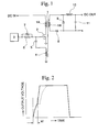
- Fig. 1 shows an embodiment of the switching circuit (switching regulator) according to the present invention.
- This switching circuit includes a transformer 1 having a primary winding 1A, a secondary winding 1B, and an auxiliary winding 4.
- the primary winding 1 A and the secondary winding 1B are insulated from each other, and the auxiliary winding 4 is provided in parallel with the primary winding 1A and the secondary winding 1B.
- a voltage-driven main switching element 2 which may be an FET, is connected in serial to the primary winding 1A of the transformer 1.
- the gate (control terminal) of the switching element 2 is connected to an output of a drive circuit 3 via a parallel circuit consisting of a resistor 6 and a diode 7.
- the output of the auxiliary winding 4 is connected to the gate of the main switching element 2 via a capacitor 5 with positive feedback.
- two diodes 8 and 9, a choke coil 10, and a capacitor 11 are connected to the secondary winding 1B of the transformer 1, so that the switching circuit outputs a DC current.
- the present invention is not restricted to this structure, and another circuit may be connected to the secondary winding 1B.
- the drive circuit 3 outputs pulse signals while controlling the frequency of the pulse signals based on the output voltage of the switching circuit.
- a pulse signal is input to the gate of the main switching element 2 from the drive circuit 3, the main switching element 2 is switched ON, and current flows to the primary winding 1A of the transformer 1.
- the voltage of the gate of the main switching element 2 reaches a threshold value at time "td”
- the intensity of the signal sent from the drive circuit 3 attenuates, and the rise of the output voltage of the switching circuit is about to slow down.
- the auxiliary winding 4 generates current.
- the above embodiment is an example of forward converter.
- the present invention can be applied in any switching circuit that includes a voltage-driven main switching element connected in serial to the winding of a transformer, the primary and secondary windings thereof being isolated.
- a resistor can also be connected in series to the capacitor 5.
- the present invention it is possible to shorten the switching transition interval of the switching element and decrease the switching loss by connecting the output of the auxiliary winding of the transformer via a capacitor so that there is no dependence on the switching speed of a control circuit and the output impedance of the drive circuit, and positive feedback from the transformer is applied when the gate of the switching element exceeds a threshold value.
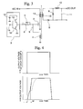
- Fig. 3 shows another embodiment of the present invention.
- the drive circuit 3 includes a referential DC source 12 and a buffer consisting of an npn transistor 13 and a pnp transistor 14.
- the emitters of the transistors 13 and 14 are connected to the diode 7 and the resistor 6.
- the collector of the transistor 13 is connected to the referential DC source 12, the collector of the transistor 14 is earthed, and an input terminal 15 is connected to the gates of the transistors 13 and 14.
- the drive circuit 3 outputs square waves at predetermined intervals as shown in the upper graph of Fig. 4, and the switching circuit outputs DC voltage as shown in the lower graph of Fig. 4.
- Other structures are the same as those of the embodiment shown in Fig. 1.
- the drive circuit which can be applied to the present invention is not restricted to that shown in Fig. 3, and any modifications are possible.
- Fig. 5 shows another embodiment of the present invention.
- the resistor 6 is connected between the capacitor 5 and the auxiliary winding 4 instead of being connected parallel to the diode 7.
- Other structures are the same as those of the embodiment shown in Fig. 3. This embodiment can provide the same effect as the above-mentioned embodiments.
Landscapes
- Engineering & Computer Science (AREA)
- Power Engineering (AREA)
- Dc-Dc Converters (AREA)
Applications Claiming Priority (2)
| Application Number | Priority Date | Filing Date | Title |
|---|---|---|---|
| JP2002134845 | 2002-05-10 | ||
| JP2002134845 | 2002-05-10 |
Publications (2)
| Publication Number | Publication Date |
|---|---|
| EP1361652A2 true EP1361652A2 (de) | 2003-11-12 |
| EP1361652A3 EP1361652A3 (de) | 2004-09-29 |
Family
ID=29244217
Family Applications (1)
| Application Number | Title | Priority Date | Filing Date |
|---|---|---|---|
| EP03252888A Withdrawn EP1361652A3 (de) | 2002-05-10 | 2003-05-08 | Schaltschaltung |
Country Status (2)
| Country | Link |
|---|---|
| US (1) | US6903943B2 (de) |
| EP (1) | EP1361652A3 (de) |
Cited By (2)
| Publication number | Priority date | Publication date | Assignee | Title |
|---|---|---|---|---|
| WO2014095201A1 (de) * | 2012-12-17 | 2014-06-26 | Phoenix Contact Gmbh & Co Kg | Schaltnetzteil mit einer kaskodenschaltung |
| CN110281652A (zh) * | 2018-03-19 | 2019-09-27 | 富士施乐株式会社 | 容性负载驱动电路和图像形成设备 |
Families Citing this family (6)
| Publication number | Priority date | Publication date | Assignee | Title |
|---|---|---|---|---|
| JP2004015886A (ja) * | 2002-06-05 | 2004-01-15 | Shindengen Electric Mfg Co Ltd | 同期整流の駆動回路 |
| JP2004072826A (ja) | 2002-08-01 | 2004-03-04 | Shindengen Electric Mfg Co Ltd | 同期整流回路 |
| US8891252B2 (en) | 2011-06-08 | 2014-11-18 | Lear Corporation | Offline power supply and apparatus for charging a plug-in vehicle |
| GB2493562B (en) * | 2011-08-12 | 2018-10-17 | E2V Tech Uk Limited | Drive circuit and method for a gated semiconductor switching device |
| US8779717B2 (en) | 2011-12-02 | 2014-07-15 | Lear Corporation | Offline power supply and charging apparatus |
| CN103812478A (zh) * | 2014-01-28 | 2014-05-21 | 庄景阳 | 触发电路的电流同向控制装置 |
Family Cites Families (12)
| Publication number | Priority date | Publication date | Assignee | Title |
|---|---|---|---|---|
| US3708743A (en) | 1971-08-04 | 1973-01-02 | Stage Brite Inc | Circuitry for controlling a.c. power |
| JPS5925405B2 (ja) | 1975-08-28 | 1984-06-18 | 三菱電機株式会社 | 半導体スイツチ装置 |
| US4335334A (en) | 1979-09-20 | 1982-06-15 | Sanyo Electric Co., Ltd. | Horizontal scanning circuit |
| SU1762374A1 (ru) | 1990-04-09 | 1992-09-15 | Производственное объединение "Ижевский мотозавод" | Однотактный самовозбуждающийс преобразователь посто нного напр жени |
| US5313109A (en) | 1992-04-28 | 1994-05-17 | Astec International, Ltd. | Circuit for the fast turn off of a field effect transistor |
| JPH1169803A (ja) | 1997-08-11 | 1999-03-09 | Nec Corp | スイッチング電源 |
| JP3175663B2 (ja) | 1997-10-17 | 2001-06-11 | 株式会社村田製作所 | 自励発振型スイッチング電源装置 |
| JPH11206126A (ja) | 1998-01-06 | 1999-07-30 | Murata Mfg Co Ltd | 自励発振型スイッチング電源装置 |
| JP3228215B2 (ja) | 1998-03-11 | 2001-11-12 | 株式会社村田製作所 | スイッチング電源装置 |
| US6108219A (en) | 1999-01-06 | 2000-08-22 | Indigo Manufacturing Inc. | DC power converter circuit |
| DE19941449A1 (de) * | 1999-08-31 | 2001-03-01 | Braun Gmbh | Schaltnetzteil |
| JP3304944B2 (ja) | 2000-02-07 | 2002-07-22 | 株式会社ニプロン | 無停電性スイッチングレギュレータ |
-
2003
- 2003-05-06 US US10/429,748 patent/US6903943B2/en not_active Expired - Fee Related
- 2003-05-08 EP EP03252888A patent/EP1361652A3/de not_active Withdrawn
Cited By (2)
| Publication number | Priority date | Publication date | Assignee | Title |
|---|---|---|---|---|
| WO2014095201A1 (de) * | 2012-12-17 | 2014-06-26 | Phoenix Contact Gmbh & Co Kg | Schaltnetzteil mit einer kaskodenschaltung |
| CN110281652A (zh) * | 2018-03-19 | 2019-09-27 | 富士施乐株式会社 | 容性负载驱动电路和图像形成设备 |
Also Published As
| Publication number | Publication date |
|---|---|
| EP1361652A3 (de) | 2004-09-29 |
| US6903943B2 (en) | 2005-06-07 |
| US20030210118A1 (en) | 2003-11-13 |
Similar Documents
| Publication | Publication Date | Title |
|---|---|---|
| US6674658B2 (en) | Power converter including circuits for improved operational control of synchronous rectifiers therein | |
| US5926012A (en) | Gate drive circuit in power converter with condition detection device | |
| US7236041B2 (en) | Isolated gate driver circuit for power switching devices | |
| EP0817381B1 (de) | Treiberschaltung für eine Halbleitervorrichtung | |
| US5959850A (en) | Asymmetrical duty cycle flyback converter | |
| US11165422B2 (en) | Gate driver circuit with reduced power semiconductor conduction loss | |
| US4970620A (en) | FET bridge protection circuit | |
| JP7728684B2 (ja) | スイッチング回路、dc/dcコンバータおよびその制御回路 | |
| US5168182A (en) | 0-100% duty cycle, transformer isolated fet driver | |
| WO1995031852A1 (en) | Load driving device | |
| US7750720B2 (en) | Circuit arrangement and a method for galvanically separate triggering of a semiconductor switch | |
| US20210226620A1 (en) | Overcurrent protection circuit for switching element turned on and off based on control voltage | |
| EP3322093B1 (de) | Gate-trajektoriesteuerung für nullüberschwingungsumschaltung | |
| JP3409994B2 (ja) | 自己消弧形素子駆動回路 | |
| US6903943B2 (en) | Switching circuit | |
| US5687067A (en) | Low noise controller for pulse width modulated converters | |
| US4792746A (en) | Non-dissipative series voltage switching regulator having improved switching speed | |
| US6326819B1 (en) | Current buffer for gate drive | |
| US5410190A (en) | Circuit for shortening the turn-off time of a power transistor | |
| US9660637B1 (en) | Driving circuit and driving method | |
| US20210126449A1 (en) | Electronic circuit and electronic apparatus | |
| EP0177148A2 (de) | Leistungsversorgung mit MOSFET-Elementen | |
| EP0785638A2 (de) | Optischer Sender | |
| US6801065B2 (en) | Transistor output circuit, semiconductor device including transistor output circuit, and switching electric power unit having transistor output circuit | |
| US12407345B2 (en) | Switched inductive storage element to enhance gate drive at turn-off |
Legal Events
| Date | Code | Title | Description |
|---|---|---|---|
| PUAI | Public reference made under article 153(3) epc to a published international application that has entered the european phase |
Free format text: ORIGINAL CODE: 0009012 |
|
| AK | Designated contracting states |
Kind code of ref document: A2 Designated state(s): AT BE BG CH CY CZ DE DK EE ES FI FR GB GR HU IE IT LI LU MC NL PT RO SE SI SK TR |
|
| AX | Request for extension of the european patent |
Extension state: AL LT LV MK |
|
| PUAL | Search report despatched |
Free format text: ORIGINAL CODE: 0009013 |
|
| AK | Designated contracting states |
Kind code of ref document: A3 Designated state(s): AT BE BG CH CY CZ DE DK EE ES FI FR GB GR HU IE IT LI LU MC NL PT RO SE SI SK TR |
|
| AX | Request for extension of the european patent |
Extension state: AL LT LV MK |
|
| 17P | Request for examination filed |
Effective date: 20041112 |
|
| AKX | Designation fees paid |
Designated state(s): AT BE BG CH CY CZ DE DK EE ES FI FR GB GR HU IE IT LI LU MC NL PT RO SE SI SK TR |
|
| STAA | Information on the status of an ep patent application or granted ep patent |
Free format text: STATUS: THE APPLICATION HAS BEEN WITHDRAWN |
|
| 18W | Application withdrawn |
Effective date: 20090123 |