EP1361683A1 - Détecteur de fréquence radio à partir d'une fréquence optique - Google Patents
Détecteur de fréquence radio à partir d'une fréquence optique Download PDFInfo
- Publication number
- EP1361683A1 EP1361683A1 EP02290318A EP02290318A EP1361683A1 EP 1361683 A1 EP1361683 A1 EP 1361683A1 EP 02290318 A EP02290318 A EP 02290318A EP 02290318 A EP02290318 A EP 02290318A EP 1361683 A1 EP1361683 A1 EP 1361683A1
- Authority
- EP
- European Patent Office
- Prior art keywords
- optical
- guide
- interaction
- generation
- radio signal
- Prior art date
- Legal status (The legal status is an assumption and is not a legal conclusion. Google has not performed a legal analysis and makes no representation as to the accuracy of the status listed.)
- Withdrawn
Links
- 230000003287 optical effect Effects 0.000 title claims abstract description 115
- 230000003993 interaction Effects 0.000 claims abstract description 43
- 239000000463 material Substances 0.000 claims abstract description 36
- 230000008878 coupling Effects 0.000 claims abstract description 13
- 238000010168 coupling process Methods 0.000 claims abstract description 13
- 238000005859 coupling reaction Methods 0.000 claims abstract description 13
- DMLAVOWQYNRWNQ-UHFFFAOYSA-N azobenzene Chemical compound C1=CC=CC=C1N=NC1=CC=CC=C1 DMLAVOWQYNRWNQ-UHFFFAOYSA-N 0.000 claims abstract description 6
- 230000001902 propagating effect Effects 0.000 claims abstract description 3
- 238000004891 communication Methods 0.000 claims description 13
- 239000011159 matrix material Substances 0.000 claims description 5
- 239000002861 polymer material Substances 0.000 claims description 4
- 239000013307 optical fiber Substances 0.000 description 7
- 230000005855 radiation Effects 0.000 description 7
- 238000010521 absorption reaction Methods 0.000 description 5
- 238000001514 detection method Methods 0.000 description 3
- 230000005684 electric field Effects 0.000 description 3
- 238000000034 method Methods 0.000 description 3
- 229920000642 polymer Polymers 0.000 description 3
- 230000000644 propagated effect Effects 0.000 description 3
- 230000007704 transition Effects 0.000 description 3
- VYPSYNLAJGMNEJ-UHFFFAOYSA-N Silicium dioxide Chemical compound O=[Si]=O VYPSYNLAJGMNEJ-UHFFFAOYSA-N 0.000 description 2
- 230000005540 biological transmission Effects 0.000 description 2
- 238000010276 construction Methods 0.000 description 2
- 239000006185 dispersion Substances 0.000 description 2
- 238000005516 engineering process Methods 0.000 description 2
- 238000004519 manufacturing process Methods 0.000 description 2
- 229910052751 metal Inorganic materials 0.000 description 2
- 239000002184 metal Substances 0.000 description 2
- 239000004065 semiconductor Substances 0.000 description 2
- 230000003595 spectral effect Effects 0.000 description 2
- 239000000126 substance Substances 0.000 description 2
- FOQABOMYTOFLPZ-ISLYRVAYSA-N Disperse Red 1 Chemical compound C1=CC(N(CCO)CC)=CC=C1\N=N\C1=CC=C([N+]([O-])=O)C=C1 FOQABOMYTOFLPZ-ISLYRVAYSA-N 0.000 description 1
- RTAQQCXQSZGOHL-UHFFFAOYSA-N Titanium Chemical compound [Ti] RTAQQCXQSZGOHL-UHFFFAOYSA-N 0.000 description 1
- 239000004566 building material Substances 0.000 description 1
- 239000000969 carrier Substances 0.000 description 1
- 238000004132 cross linking Methods 0.000 description 1
- 238000000354 decomposition reaction Methods 0.000 description 1
- 238000010586 diagram Methods 0.000 description 1
- 230000005672 electromagnetic field Effects 0.000 description 1
- 238000000605 extraction Methods 0.000 description 1
- 229920002313 fluoropolymer Polymers 0.000 description 1
- PCHJSUWPFVWCPO-UHFFFAOYSA-N gold Chemical compound [Au] PCHJSUWPFVWCPO-UHFFFAOYSA-N 0.000 description 1
- 239000010931 gold Substances 0.000 description 1
- 229910052737 gold Inorganic materials 0.000 description 1
- 230000006698 induction Effects 0.000 description 1
- 238000003780 insertion Methods 0.000 description 1
- 230000037431 insertion Effects 0.000 description 1
- GQYHUHYESMUTHG-UHFFFAOYSA-N lithium niobate Chemical compound [Li+].[O-][Nb](=O)=O GQYHUHYESMUTHG-UHFFFAOYSA-N 0.000 description 1
- 239000013308 plastic optical fiber Substances 0.000 description 1
- 230000010287 polarization Effects 0.000 description 1
- 229920003229 poly(methyl methacrylate) Polymers 0.000 description 1
- 239000004926 polymethyl methacrylate Substances 0.000 description 1
- 230000006798 recombination Effects 0.000 description 1
- 238000005215 recombination Methods 0.000 description 1
- 230000009467 reduction Effects 0.000 description 1
- 239000000377 silicon dioxide Substances 0.000 description 1
- 238000001228 spectrum Methods 0.000 description 1
- 239000010936 titanium Substances 0.000 description 1
- 229910052719 titanium Inorganic materials 0.000 description 1
Images


Classifications
-
- G—PHYSICS
- G02—OPTICS
- G02F—OPTICAL DEVICES OR ARRANGEMENTS FOR THE CONTROL OF LIGHT BY MODIFICATION OF THE OPTICAL PROPERTIES OF THE MEDIA OF THE ELEMENTS INVOLVED THEREIN; NON-LINEAR OPTICS; FREQUENCY-CHANGING OF LIGHT; OPTICAL LOGIC ELEMENTS; OPTICAL ANALOGUE/DIGITAL CONVERTERS
- G02F2/00—Demodulating light; Transferring the modulation of modulated light; Frequency-changing of light
- G02F2/002—Demodulating light; Transferring the modulation of modulated light; Frequency-changing of light using optical mixing
-
- H—ELECTRICITY
- H04—ELECTRIC COMMUNICATION TECHNIQUE
- H04B—TRANSMISSION
- H04B10/00—Transmission systems employing electromagnetic waves other than radio-waves, e.g. infrared, visible or ultraviolet light, or employing corpuscular radiation, e.g. quantum communication
- H04B10/25—Arrangements specific to fibre transmission
- H04B10/2575—Radio-over-fibre, e.g. radio frequency signal modulated onto an optical carrier
-
- H—ELECTRICITY
- H04—ELECTRIC COMMUNICATION TECHNIQUE
- H04B—TRANSMISSION
- H04B10/00—Transmission systems employing electromagnetic waves other than radio-waves, e.g. infrared, visible or ultraviolet light, or employing corpuscular radiation, e.g. quantum communication
- H04B10/60—Receivers
- H04B10/66—Non-coherent receivers, e.g. using direct detection
-
- G—PHYSICS
- G02—OPTICS
- G02F—OPTICAL DEVICES OR ARRANGEMENTS FOR THE CONTROL OF LIGHT BY MODIFICATION OF THE OPTICAL PROPERTIES OF THE MEDIA OF THE ELEMENTS INVOLVED THEREIN; NON-LINEAR OPTICS; FREQUENCY-CHANGING OF LIGHT; OPTICAL LOGIC ELEMENTS; OPTICAL ANALOGUE/DIGITAL CONVERTERS
- G02F1/00—Devices or arrangements for the control of the intensity, colour, phase, polarisation or direction of light arriving from an independent light source, e.g. switching, gating or modulating; Non-linear optics
- G02F1/35—Non-linear optics
- G02F1/353—Frequency conversion, i.e. wherein a light beam is generated with frequency components different from those of the incident light beams
- G02F1/3534—Three-wave interaction, e.g. sum-difference frequency generation
-
- G—PHYSICS
- G02—OPTICS
- G02F—OPTICAL DEVICES OR ARRANGEMENTS FOR THE CONTROL OF LIGHT BY MODIFICATION OF THE OPTICAL PROPERTIES OF THE MEDIA OF THE ELEMENTS INVOLVED THEREIN; NON-LINEAR OPTICS; FREQUENCY-CHANGING OF LIGHT; OPTICAL LOGIC ELEMENTS; OPTICAL ANALOGUE/DIGITAL CONVERTERS
- G02F2201/00—Constructional arrangements not provided for in groups G02F1/00 - G02F7/00
- G02F2201/06—Constructional arrangements not provided for in groups G02F1/00 - G02F7/00 integrated waveguide
- G02F2201/063—Constructional arrangements not provided for in groups G02F1/00 - G02F7/00 integrated waveguide ridge; rib; strip loaded
-
- G—PHYSICS
- G02—OPTICS
- G02F—OPTICAL DEVICES OR ARRANGEMENTS FOR THE CONTROL OF LIGHT BY MODIFICATION OF THE OPTICAL PROPERTIES OF THE MEDIA OF THE ELEMENTS INVOLVED THEREIN; NON-LINEAR OPTICS; FREQUENCY-CHANGING OF LIGHT; OPTICAL LOGIC ELEMENTS; OPTICAL ANALOGUE/DIGITAL CONVERTERS
- G02F2201/00—Constructional arrangements not provided for in groups G02F1/00 - G02F7/00
- G02F2201/12—Constructional arrangements not provided for in groups G02F1/00 - G02F7/00 electrode
- G02F2201/127—Constructional arrangements not provided for in groups G02F1/00 - G02F7/00 electrode travelling wave
-
- G—PHYSICS
- G02—OPTICS
- G02F—OPTICAL DEVICES OR ARRANGEMENTS FOR THE CONTROL OF LIGHT BY MODIFICATION OF THE OPTICAL PROPERTIES OF THE MEDIA OF THE ELEMENTS INVOLVED THEREIN; NON-LINEAR OPTICS; FREQUENCY-CHANGING OF LIGHT; OPTICAL LOGIC ELEMENTS; OPTICAL ANALOGUE/DIGITAL CONVERTERS
- G02F2202/00—Materials and properties
- G02F2202/02—Materials and properties organic material
- G02F2202/022—Materials and properties organic material polymeric
-
- G—PHYSICS
- G02—OPTICS
- G02F—OPTICAL DEVICES OR ARRANGEMENTS FOR THE CONTROL OF LIGHT BY MODIFICATION OF THE OPTICAL PROPERTIES OF THE MEDIA OF THE ELEMENTS INVOLVED THEREIN; NON-LINEAR OPTICS; FREQUENCY-CHANGING OF LIGHT; OPTICAL LOGIC ELEMENTS; OPTICAL ANALOGUE/DIGITAL CONVERTERS
- G02F2202/00—Materials and properties
- G02F2202/07—Materials and properties poled
Definitions
- This invention relates to radio frequency modulated optical radiation and, more particularly, to apparatus for detecting radio signals modulated on optical signals.
- Radio frequency modulated optical fibres systems such as those described in US Patent specification N° 5 917 636 enable a mobile network to be built covering wide areas. These systems are capable of accepting continuous increase in demand in terms of data rate and free spectrum range and of expansion of the equipment and infrastructure installed.
- the increase of frequency of these systems enables a reduction in the size of the antennae and devices used in the radio frequency part of the network and an increase in the bandwidth of the whole system.
- two spectral ranges of 62-63GHz and 65-66GHz which are still unallocated by ITU, have been identified within the framework of the NBS project (RACE 2067) as particularly suitable for such systems.
- the present invention is applicable to these frequency ranges and other frequencies, especially but not exclusively in the so-called millimetric radio frequency ranges, where the wavelength of the radio signal in free air is of the order of one to ten millimetres.
- Such radio signals may be subject to strong absorption by the atmosphere and by common building materials, so that it is of particular interest transmission for the radio signals to be modulated onto an optical signal that is guided in an optical fibre from a source to a so-called pico-cell, where the radio signal may be detected and, if desired, radiated over a relatively short distance.
- generation of the modulated optical signals is preferably obtained by combining two phase-correlated optical carriers which are generated in a dual-frequency laser transmitter with a frequency offset equal to the desired microwave frequency of the radio carrier signal.
- the two optical signals are then transmitted through optical fibre and the radio signal is recovered in a detector.
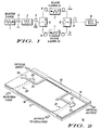
- FIG. 1 An example of a communication system of this kind, which may be used in a system in accordance with the present invention, is shown in Figure 1 and comprises, at the transmitter end, a master laser 1, connected by optical fibre 2 to a radio frequency modulator 3, which in turn is connected by optical fibre 4 to a beam splitter 5.
- the two optical signals from the beam splitter 5 are connected by optical fibres 6 to two slave lasers 7 tuned to frequencies spaced apart by an amount equal to the radio signal frequency, which act as filters to generate optical signals with a high degree of phase correlation and spectral purity.
- the outputs of the slave lasers 7 are connected to a recombination device 8 before transmission over the optical fibre output line 9.
- the system comprises a detector 10 that receives the optical signals in the optical fibre line 9 and demodulates the radio signals.
- the article "High frequency polymer modulators with integrated finline transitions and low V ⁇ " in IEEE Photonics Technology Letters, Volume 11 pages 54 to 56 discloses the use of a non-linear optical polymer material in a radio frequency modulator for the optical signal, the material being disposed between two electrodes terminating a radio frequency microstrip wave-guide.
- the radio signal detector described in that article is a photodetector.
- the present invention provides an optical to radio frequency detector and communication apparatus as described in the accompanying claims.
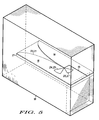
- FIG. 2 to 6 of the drawings show apparatus for converting between optical and radio frequency signals in accordance with one embodiment of the present invention.
- the apparatus shown in Figures 2 to 6 of the drawings is an optical to radio frequency detector and this embodiment of the invention is described with reference to a detector; however, it will be appreciated that similar design principles can be applied to a modulator for modulating an optical signal with a radio frequency signal.
- the design principles are also applicable to a transceiver, that is to say a device that receives optical signals modulated by a first radio signals and detects the first radio signals, and modulates the optical signals with a second radio signal that is transmitted elsewhere.
- Figure 1 of the drawings shows a communication system as described above including a modulator 3 and a detector 10.
- the detector 10 of the system is of the kind illustrated in Figures 2 to 6 of the accompanying drawings.
- the modulator is also of the kind shown in Figures 2 to 6 of the drawings, but with a single optical input signal and a radio frequency input signal instead of the two optical input signals and radio frequency output signal of the detector.
- the detector is a passive detector comprising an optical ridge wave-guide.
- a construction of an optical ridge wave-guide is described in the article "The single-mode condition for semiconductor wave-guides with large cross-section" in the Journal of Light Wave Technology, Volume 16, pages 1851 to 1853, for example.
- the optical guide used is based on the principle of total reflection at the interface between two mediums of different refractive index.
- the optical ridge wave-guide comprises upper and lower buffer layers 11 and 12.
- An electro-optic core is positioned in intimate contact between the upper and lower buffer layers 11 and 12, the electro-optic core 10 comprising a layer 13 of thickness substantially less than the wavelength of the optical radiation and a ridge 14 of thickness comparable to the wavelength of the optical radiation and of width greater than the wavelength of the optical radiation.
- the wavelength of the optical radiation is 1.55 microns
- the thickness of the layer 13 is 0.2 microns
- the thickness of the ridge 14 is 1.5 microns
- the width of the ridge being 4 microns.
- the interaction material of the electro-optic guide 13, 14 presents a second-order non-linear optical polarisation characteristic to the propagation of the optical signal components and more particularly is a dipolar material presenting non-centre-symmetric interaction characteristics in a host matrix polymer material.
- a suitable interaction material of this kind comprises electrically orientated diazobenzene.
- the electrically orientated diazobenzene is an active chromophore "Disperse Red 1" grafted to polymethylmetacrylate as host matrix ("PMMA-DR1").
- PMMA-DR1 active chromophore
- the chemical formula of PMMA-DR1 is shown in Figure 4, the left hand side of the formula being the active dipolar DR1 and the right hand side being the host PMMA.
- a molecule of this type placed in an electric field orients in such a way as to align with the field.
- an orientated material can be obtained in which the polar molecules are statistically directed in similar directions to give second order non-linear optical polarisation properties, and in particular non-centre-symmetric properties.
- the electro-optic core 13, 14 is formed in PMMA-DR1.
- the component is heated to the vitreous transition point of the electro-optic core polymer, approximately 120°C.
- An intense electric field is applied to the metal layers used as electrodes. The electric field is maintained subsequently while the temperature is reduced towards ambient temperature.
- the buffer layers 11 and 12 are produced in fluorinated polymers "AVO14" and “AVO01” described in the article "Fabrication of low refractive index low loss fluorinated self-cross linking polymer waveguides for optical devices" in the Proceedings of the 7 th International Plastic Optical Fibres Conference 1998, pages 316 to 323. These materials are chosen for their refractive index, which is less than that of the electro-optic core. At the wavelength of the optical radiation in the present example, 1.55 microns, the refractive index of PMMA-DR1 is 1.5965, the refractive index of AVO01 is 1.4466 and that of AVO14 is 1.4009.
- the electro-optic core ridge 14 is connected with input and output optical fibres (not shown) by respective linear tapers (not shown), which adapt the shape and size of the optical fibre (typically diameter 10 microns) to the shape (rectangular cross-section) and size (approximately 4 microns) of the electro-optic core ridge 14 while reducing insertion and extraction losses.
- the device shown in the drawings also includes a radio signal guide in travelling wave coupling with the optical guide formed by the electro-optic core 10.
- Various radio signal wave-guides may be used, such as a strip-line in which a strip extends between two ground planes, or a coplanar wave-guide in which a strip extends in the same plane as two lateral grounded strips, or a grounded coplanar wave-guide in which a coplanar wave-guide extends parallel to a grounded plane.
- the radio signal guide is a microstrip guide comprising a strip of width approximately 15 microns, compared with a width of approximately 4 microns for the optical wave-guide electro-optic core ridge 14, juxtaposed with a ground plane metallic layer 16 on the opposite side of the electro-optic core ridge 14.
- the spacing and width of the strip 15 and ground plane layer 16 are chosen so that the impedance of the microstrip at the radio signal frequency (60GHz in this example) are compatible with standard wave-guides such as the WR15 wave-guide (50ohms).
- the standard dimensions of a WR15 wave-guide are as follows: Band Frequ. range Internal dims (mm) External dims (mm) Cut-off frequ. Losses (dB/m) width height width height V 50-75 GHz 0.3759 0.1879 0.579 0.391 39.9 GHz 0.188
- the strip 15 is closely juxtaposed with the top surface of the upper buffer 11 and the ground plane 16 is closely juxtaposed with the bottom surface of the lower buffer 12.
- the length over which the microstrip 15 is in close coupling with the optical guide is chosen to be at least approximately equal to the wavelength of the radio signal, that is to say, at least 5 millimetres at the radio signal frequency of 60GHz in this example; in the preferred embodiment of the invention, the optical/radio interaction length for this frequency is 1.3cm. In this way, a travelling wave coupling is obtained that is found to be particularly effective for the efficiency of the device.
- the dimensions of the elements of the device and the characteristics of the materials used are chosen so that the propagation velocities of the optical signal components in the optical guide and of the radio signal in the radio signal guide are substantially equal. Again, this characteristic is found to be important for the efficiency of detection (or modulation in the case of a modulator).
- E and H are respectively the electrical and induction fields.
- guided mode formalism is used, where the different fields are split on an orthogonal basis constituted by the local modes, as shown by the following equation:
- E rad and H rad are the radiating parts of the electromagnetic field. Then, using the orthogonal properties of this decomposition, the variation of the amplitude of each wavelength is deduced from (1) and (3):
- the ⁇ coefficients represent the overlap of the three fields. Finally account is taken of the absorption of the propagation medium by introducing a complex value for ⁇ k in the treatment of the system (4).
- the ground plane 16 is formed from a layer of gold deposited on a layer of titanium that is itself deposited on a layer of silica 17 serving as a support.
- the microstrip radio signal guide 15 extending parallel to and juxtaposed with the optical guide 14 is connected with external radio signal wave-guides (one of which is shown at 18 in Figures 5 and 6 of WR15 type (standard wave-guides for 50 to 75 GHz radio frequencies).
- the WR15 wave-guides extend perpendicularly to the length of the microstrip radio signal guide 15 and the optical guide 14 and parallel to the ground plane 16.
- Transition radio signal guide elements 20 and 21 are formed in the material of the ground plane 16 and present progressively varying cross sections to match the propagation characteristics of the microstrip with the WR15 wave-guides. More specifically, the guide elements 20 and 21 comprise "Vivaldi antenna" openings in the ground planes 16 of trumpet shape, of which the small end is of similar width to the microstrip 15 and the large end is of similar width to the corresponding width ('height') of the wave-guide WR15, such as 18.
- the Vivaldi antenna 21 is connected with the receiver circuit elements (for example, to a re-transmission circuit) while the Vivaldi antenna 20 is connected to an element presenting a matching load to the microstrip 15, to ensure that it functions in balanced conditions.
- the microstrip element 15 traverses the small end of the Vivaldi antennas 20 and 21, spaced from them by the thickness of the stacked buffer layers 11 and 12 and the electro-optic layer 13, 14.
- the microstrip 15 includes extensions 22 and 23 that are parallel with, but staggered relative to, the part of the microstrip 15 in radio signal coupling relationship with the optical guide 14.
- the small ends of the Vivaldi antennas 20 and 21 are also spaced relative to the optical guide 14.
- the small ends of the Vivaldi antennas 20 and 21 are disposed directly beneath the optical guide 14 and the microstrip-line 15 is entirely in line with the optical guide 14 and in radio signal coupling relationship therewith.
- radio signal frequency resonators 24, 25 are formed in the shape of quadrant (or "fan") resonators as extensions of the ends of the microstrip 15 and resonators 26, 27 are formed as extensions of the openings at the small ends of the Vivaldi antennas 20 and 21.
- the resonators are designed with dimensions such that they present termination impedances matched to the impedances of the microstrip 15 and the Vivaldi antenna 20,21, respectively, at the operating radio frequency. They effectively minimise the termination reflection coefficient in the plane of propagation of the radio signal in the corresponding element.
- the Vivaldi antennas 20 and 21 are preferably 7.8 microns wide at the small end and 1.879mm wide at the wide end and 3mm long.
- the resonators 26 and 27 of the Vivaldi antennas are preferably of radius 0.56mm and the resonators 24 and 25 of the microstrip are preferably of radius 0.62mm.
- two optical signal components having frequencies that differ by an amount corresponding to the radio signal carrier frequency are applied to the optical input of the optical guide 14.
- the two optical components interact in the second-order non-linear optical polarisation material of the electro-optical core 14.
- the close coupling of the microstrip 15 and ground plane 16 with the optical guide 14 causes the radio frequency signals that result to be induced in the microstrip-line 15.
- the line 15, together with its extensions 22 and 23 in the case of the embodiment shown in Figure 2, and the Vivaldi antennas 20 and 21 extending within the WR15 wave-guides as shown in Figure 4 transmit the radio frequency signal to the WR15 wave-guide 18 and the radio signal is received in the wave-guide.
- a radio signal propagated in the WR15 wave-guide with a single optical component propagated in the optical guide modulates the optical component so that at the output of the optical wave-guide two optical components are propagated.
- the output power of the electrical signal in the case of the detector device shown in the drawings is proportional to the square of the radio frequency, so that substantially higher efficiencies are obtained than in other devices whose efficiency reduces with frequency.
- the output of the radio signal is also proportional to the square of the interaction link and to the square of the input power of the optical signal: consequently the device is more efficient the more intense the optical signals but, concerning the interaction links, absorption of the optical signals in the optical guide limits the length of the optimum interaction link.
Landscapes
- Physics & Mathematics (AREA)
- Electromagnetism (AREA)
- Engineering & Computer Science (AREA)
- Computer Networks & Wireless Communication (AREA)
- Signal Processing (AREA)
- General Physics & Mathematics (AREA)
- Nonlinear Science (AREA)
- Optics & Photonics (AREA)
- Optical Communication System (AREA)
- Optical Modulation, Optical Deflection, Nonlinear Optics, Optical Demodulation, Optical Logic Elements (AREA)
Priority Applications (5)
| Application Number | Priority Date | Filing Date | Title |
|---|---|---|---|
| EP02290318A EP1361683A1 (fr) | 2002-02-08 | 2002-02-08 | Détecteur de fréquence radio à partir d'une fréquence optique |
| PCT/EP2003/000224 WO2003067321A1 (fr) | 2002-02-08 | 2003-01-13 | Detecteur de frequences optiques-radioelectriques |
| US10/504,010 US7877015B2 (en) | 2002-02-08 | 2003-01-13 | Optical to radio frequency detector |
| AU2003244489A AU2003244489A1 (en) | 2002-02-08 | 2003-01-13 | Optical to radio frequency detector |
| TW092101463A TWI321257B (en) | 2002-02-08 | 2003-01-23 | Optical to radio frequency detector |
Applications Claiming Priority (1)
| Application Number | Priority Date | Filing Date | Title |
|---|---|---|---|
| EP02290318A EP1361683A1 (fr) | 2002-02-08 | 2002-02-08 | Détecteur de fréquence radio à partir d'une fréquence optique |
Publications (1)
| Publication Number | Publication Date |
|---|---|
| EP1361683A1 true EP1361683A1 (fr) | 2003-11-12 |
Family
ID=27675762
Family Applications (1)
| Application Number | Title | Priority Date | Filing Date |
|---|---|---|---|
| EP02290318A Withdrawn EP1361683A1 (fr) | 2002-02-08 | 2002-02-08 | Détecteur de fréquence radio à partir d'une fréquence optique |
Country Status (5)
| Country | Link |
|---|---|
| US (1) | US7877015B2 (fr) |
| EP (1) | EP1361683A1 (fr) |
| AU (1) | AU2003244489A1 (fr) |
| TW (1) | TWI321257B (fr) |
| WO (1) | WO2003067321A1 (fr) |
Families Citing this family (4)
| Publication number | Priority date | Publication date | Assignee | Title |
|---|---|---|---|---|
| EP1361683A1 (fr) * | 2002-02-08 | 2003-11-12 | Motorola, Inc. | Détecteur de fréquence radio à partir d'une fréquence optique |
| ATE525816T1 (de) * | 2006-05-12 | 2011-10-15 | Gigaset Communications Gmbh | Verfahren zum senden von optisch übertragenen daten über eine funkantenne und vorrichtung |
| US20090116843A1 (en) * | 2006-05-12 | 2009-05-07 | Siemens Home And Office Communication Devices Gmbh | Device for Transmitting and Receiving Data and Corresponding Operating Method |
| US8816284B2 (en) * | 2010-03-30 | 2014-08-26 | Lawrence Livermore National Security, Llc. | Room-temperature quantum noise limited spectrometry and methods of the same |
Citations (3)
| Publication number | Priority date | Publication date | Assignee | Title |
|---|---|---|---|---|
| US5251053A (en) * | 1990-06-15 | 1993-10-05 | Alcatel N.V. | Radio communication system |
| US5917636A (en) * | 1994-07-29 | 1999-06-29 | British Telecommunications Public Limited Company | Generation of radio frequency modulated optical radiation |
| WO2000077956A1 (fr) * | 1999-06-10 | 2000-12-21 | Fiberspace, Inc. | Procede et appareil d'utilisation de techniques de melange d'hyperfrequences/rf pour selectionner une bande donnee d'une transmission optique |
Family Cites Families (10)
| Publication number | Priority date | Publication date | Assignee | Title |
|---|---|---|---|---|
| US5327149A (en) * | 1992-05-18 | 1994-07-05 | Hughes Missile Systems Company | R.F. transparent RF/UV-IR detector apparatus |
| US5317666A (en) * | 1992-09-29 | 1994-05-31 | Eastman Kodak Company | Waveguide nonlinear optical frequency converter with integral modulation and optimization means |
| US5585957A (en) * | 1993-03-25 | 1996-12-17 | Nippon Telegraph And Telephone Corporation | Method for producing various semiconductor optical devices of differing optical characteristics |
| US5515463A (en) * | 1995-03-10 | 1996-05-07 | Hewlett-Packard Company | Multi-branch microwave line for electro-optical devices |
| US5710651A (en) * | 1995-12-13 | 1998-01-20 | California Institute Of Technology | Remote millimeter-wave antenna fiber optic communication system using dual optical signal with millimeter-wave beat frequency |
| US6522793B1 (en) * | 2001-11-21 | 2003-02-18 | Andrei Szilagyi | Low voltage electro-optic modulator with integrated driver |
| DE60204210T2 (de) * | 2002-02-08 | 2005-10-13 | Freescale Semiconductor, Inc., Austin | Konvertierung zwischen optischen und Hochfrequenzsignalen |
| EP1361683A1 (fr) * | 2002-02-08 | 2003-11-12 | Motorola, Inc. | Détecteur de fréquence radio à partir d'une fréquence optique |
| JP3841793B2 (ja) * | 2004-02-26 | 2006-11-01 | 独立行政法人情報通信研究機構 | 無線光融合通信システムにおける周波数変換方法及び基地局 |
| KR100703367B1 (ko) * | 2005-09-12 | 2007-04-03 | 삼성전자주식회사 | 무선 원격 기지국과 그를 이용한 피코-셀 시스템 |
-
2002
- 2002-02-08 EP EP02290318A patent/EP1361683A1/fr not_active Withdrawn
-
2003
- 2003-01-13 WO PCT/EP2003/000224 patent/WO2003067321A1/fr not_active Ceased
- 2003-01-13 US US10/504,010 patent/US7877015B2/en not_active Expired - Lifetime
- 2003-01-13 AU AU2003244489A patent/AU2003244489A1/en not_active Abandoned
- 2003-01-23 TW TW092101463A patent/TWI321257B/zh not_active IP Right Cessation
Patent Citations (3)
| Publication number | Priority date | Publication date | Assignee | Title |
|---|---|---|---|---|
| US5251053A (en) * | 1990-06-15 | 1993-10-05 | Alcatel N.V. | Radio communication system |
| US5917636A (en) * | 1994-07-29 | 1999-06-29 | British Telecommunications Public Limited Company | Generation of radio frequency modulated optical radiation |
| WO2000077956A1 (fr) * | 1999-06-10 | 2000-12-21 | Fiberspace, Inc. | Procede et appareil d'utilisation de techniques de melange d'hyperfrequences/rf pour selectionner une bande donnee d'une transmission optique |
Non-Patent Citations (6)
| Title |
|---|
| BRIDGES W.B.; SHEEHY F.T.; SCHAFFNER J.H.: "WAVE-COUPLED LINBO3 ELECTROOPTIC MODULATOR FOR MICROWAVE AND MILLIMETER-WAVE MODULATION", IEEE PHOTONICS TECHNOLOGY LETTERS, vol. 3, no. 2, 1 February 1991 (1991-02-01), IEEE SERVICE CENTER, PISCATAWAY, NJ, US, pages 133 - 135, XP000203007, ISSN: 1041-1135, DOI: 10.1109/68.76865 * |
| DUBOVITSKY S.; CHUYANOV V.; GARNER S.; STEIER W.H., INTERNATIONAL TOPICAL MEETING ON MICROWAVE PHOTONICS, 1998. MWP '98. PRINCETON, NJ, USA 12-14 OCT. 1998, 12 October 1998 (1998-10-12), PISCATAWAY, NJ, USA, pages 85 - 86, ISBN: 0-7803-4936-9 * |
| KATO K: "ULTRAWIDE-BAND/HIGH-FREQUENCY PHOTODETECTORS", IEEE TRANSACTIONS ON MICROWAVE THEORY AND TECHNIQUES, IEEE INC. NEW YORK, US, vol. 47, no. 7, July 1999 (1999-07-01), pages 1265 - 1280, XP000846032, ISSN: 0018-9480 * |
| TENG C.C.: "TRAVELING-WAVE POLYMERIC OPTICAL INTENSITY MODULATOR WITH MORE THAN 40 GHZ OF 3-DB ELECTRICAL BANDWIDTH", APPLIED PHYSICS LETTERS, AIP, AMERICAN INSTITUTE OF PHYSICS, vol. 60, no. 13, 30 March 1992 (1992-03-30), MELVILLE, NY, US, pages 1538 - 1540, XP000273295, ISSN: 0003-6951, DOI: 10.1063/1.107482 * |
| WANG W. ET AL: "40-GHZ POLYMER ELECTROOPTIC PHASE MODULATORS", IEEE PHOTONICS TECHNOLOGY LETTERS, vol. 7, no. 6, 1 June 1995 (1995-06-01), IEEE SERVICE CENTER, PISCATAWAY, NJ, US, pages 638 - 640, XP000510202, ISSN: 1041-1135, DOI: 10.1109/68.388749 * |
| WANG WENSHEN ET AL: "TRAVELING WAVE ELECTRO-OPTIC PHASE MODULATOR USING CROSS-LINKED NONLINEAR OPTICAL POLYMER", APPLIED PHYSICS LETTERS, AIP, AMERICAN INSTITUTE OF PHYSICS, vol. 65, no. 8, 22 August 1994 (1994-08-22), MELVILLE, NY, US, pages 929 - 931, XP000463527, ISSN: 0003-6951, DOI: 10.1063/1.112152 * |
Also Published As
| Publication number | Publication date |
|---|---|
| WO2003067321A1 (fr) | 2003-08-14 |
| US20070058977A1 (en) | 2007-03-15 |
| TWI321257B (en) | 2010-03-01 |
| AU2003244489A1 (en) | 2003-09-02 |
| TW200302950A (en) | 2003-08-16 |
| US7877015B2 (en) | 2011-01-25 |
Similar Documents
| Publication | Publication Date | Title |
|---|---|---|
| US5644664A (en) | Fiber optic digital transmission system | |
| US5208697A (en) | Microwave frequency range electro-optic modulator with efficient input coupling and smooth wideband frequency response | |
| CN1152980A (zh) | 射频调制的光辐射的生成 | |
| EP1335239B1 (fr) | Conversion entre des signaux optiques et radioélectriques | |
| WO2000068731A2 (fr) | Modulation optique externe employant des circuits de compensation non co-lineaires | |
| Yu et al. | Hybrid integration between resonant tunneling diodes and unclad microphotonic diplexer for dual-channel coherent terahertz receiver | |
| US7016554B2 (en) | Optical modulator | |
| Heni et al. | Plasmonic PICs—Terabit Modulation on the Micrometer Scale | |
| AU2002325673A1 (en) | Optical modulator | |
| CN114567384B (zh) | 通用型硅基光子毫米波/太赫兹芯片及其传递系统和方法 | |
| US7877015B2 (en) | Optical to radio frequency detector | |
| Jäger | 1 Microwave Photonics | |
| Loi et al. | Low-loss 1.3-μm MQW electroabsorption modulators for high-linearity analog optical links | |
| Maury et al. | Remote upconversion in microwave fiber optic links employing an unbalanced Mach-Zehnder interferometer | |
| Mortazy et al. | Mode coupling between substrate integrated waveguide and coplanar waveguide for traveling-wave electrooptical modulator | |
| HK1075498B (en) | Conversion between optical and radio frequency signals | |
| Wijayanto et al. | Metamaterial antenna integrated to LiNbO3 optical modulator for millimeter-wave-photonic links | |
| EP4715462A1 (fr) | Modulateur optique à guide d'ondes | |
| Devaux et al. | Optical processing with electroabsorption modulators | |
| Lu et al. | A Broadband Lithium Tantalate-on-Silicon Nitride Heterogeneous Modulator for Optical and Terahertz Communications and Radar Sensing | |
| JP3225113B2 (ja) | 周波数ミキサ装置 | |
| Akaike | Trends of research on microwaves/optics in Japan | |
| KAWANO | Improvement of the Performance of a Shielded Velocity-Matched Ti: LiNbO 3 Optical Modulator by Using a Ridge Structure | |
| JPH077322A (ja) | スロットアンテナ装置 | |
| Knoesen et al. | High-bandwidth polymer in-line fiber modulator |
Legal Events
| Date | Code | Title | Description |
|---|---|---|---|
| PUAI | Public reference made under article 153(3) epc to a published international application that has entered the european phase |
Free format text: ORIGINAL CODE: 0009012 |
|
| AK | Designated contracting states |
Kind code of ref document: A1 Designated state(s): AT BE CH CY DE DK ES FI FR GB GR IE IT LI LU MC NL PT SE TR |
|
| AX | Request for extension of the european patent |
Extension state: AL LT LV MK RO SI |
|
| 17P | Request for examination filed |
Effective date: 20040512 |
|
| AKX | Designation fees paid |
Designated state(s): AT BE CH CY DE DK ES FI FR GB GR IE IT LI LU MC NL PT SE TR |
|
| GRAP | Despatch of communication of intention to grant a patent |
Free format text: ORIGINAL CODE: EPIDOSNIGR1 |
|
| GRAJ | Information related to disapproval of communication of intention to grant by the applicant or resumption of examination proceedings by the epo deleted |
Free format text: ORIGINAL CODE: EPIDOSDIGR1 |
|
| 17Q | First examination report despatched |
Effective date: 20041021 |
|
| RAP1 | Party data changed (applicant data changed or rights of an application transferred) |
Owner name: FREESCALE SEMICONDUCTOR, INC. |
|
| 17Q | First examination report despatched |
Effective date: 20041021 |
|
| STAA | Information on the status of an ep patent application or granted ep patent |
Free format text: STATUS: THE APPLICATION IS DEEMED TO BE WITHDRAWN |
|
| 18D | Application deemed to be withdrawn |
Effective date: 20070918 |