EP1365488A2 - Verfahren zum Verpacken einer Subträgerbaugruppe - Google Patents
Verfahren zum Verpacken einer Subträgerbaugruppe Download PDFInfo
- Publication number
- EP1365488A2 EP1365488A2 EP03016397A EP03016397A EP1365488A2 EP 1365488 A2 EP1365488 A2 EP 1365488A2 EP 03016397 A EP03016397 A EP 03016397A EP 03016397 A EP03016397 A EP 03016397A EP 1365488 A2 EP1365488 A2 EP 1365488A2
- Authority
- EP
- European Patent Office
- Prior art keywords
- submount
- assembly
- package
- electro
- laser diode
- Prior art date
- Legal status (The legal status is an assumption and is not a legal conclusion. Google has not performed a legal analysis and makes no representation as to the accuracy of the status listed.)
- Granted
Links
Images



Classifications
-
- H—ELECTRICITY
- H01—ELECTRIC ELEMENTS
- H01S—DEVICES USING THE PROCESS OF LIGHT AMPLIFICATION BY STIMULATED EMISSION OF RADIATION [LASER] TO AMPLIFY OR GENERATE LIGHT; DEVICES USING STIMULATED EMISSION OF ELECTROMAGNETIC RADIATION IN WAVE RANGES OTHER THAN OPTICAL
- H01S3/00—Lasers, i.e. devices using stimulated emission of electromagnetic radiation in the infrared, visible or ultraviolet wave range
- H01S3/02—Constructional details
- H01S3/025—Constructional details of solid state lasers, e.g. housings or mountings
-
- H—ELECTRICITY
- H01—ELECTRIC ELEMENTS
- H01S—DEVICES USING THE PROCESS OF LIGHT AMPLIFICATION BY STIMULATED EMISSION OF RADIATION [LASER] TO AMPLIFY OR GENERATE LIGHT; DEVICES USING STIMULATED EMISSION OF ELECTROMAGNETIC RADIATION IN WAVE RANGES OTHER THAN OPTICAL
- H01S3/00—Lasers, i.e. devices using stimulated emission of electromagnetic radiation in the infrared, visible or ultraviolet wave range
- H01S3/02—Constructional details
- H01S3/04—Arrangements for thermal management
- H01S3/042—Arrangements for thermal management for solid state lasers
-
- H—ELECTRICITY
- H01—ELECTRIC ELEMENTS
- H01S—DEVICES USING THE PROCESS OF LIGHT AMPLIFICATION BY STIMULATED EMISSION OF RADIATION [LASER] TO AMPLIFY OR GENERATE LIGHT; DEVICES USING STIMULATED EMISSION OF ELECTROMAGNETIC RADIATION IN WAVE RANGES OTHER THAN OPTICAL
- H01S3/00—Lasers, i.e. devices using stimulated emission of electromagnetic radiation in the infrared, visible or ultraviolet wave range
- H01S3/05—Construction or shape of optical resonators; Accommodation of active medium therein; Shape of active medium
- H01S3/06—Construction or shape of active medium
- H01S3/0627—Construction or shape of active medium the resonator being monolithic, e.g. microlaser
-
- H—ELECTRICITY
- H01—ELECTRIC ELEMENTS
- H01S—DEVICES USING THE PROCESS OF LIGHT AMPLIFICATION BY STIMULATED EMISSION OF RADIATION [LASER] TO AMPLIFY OR GENERATE LIGHT; DEVICES USING STIMULATED EMISSION OF ELECTROMAGNETIC RADIATION IN WAVE RANGES OTHER THAN OPTICAL
- H01S5/00—Semiconductor lasers
- H01S5/02—Structural details or components not essential to laser action
- H01S5/022—Mountings; Housings
- H01S5/02208—Mountings; Housings characterised by the shape of the housings
-
- H—ELECTRICITY
- H01—ELECTRIC ELEMENTS
- H01S—DEVICES USING THE PROCESS OF LIGHT AMPLIFICATION BY STIMULATED EMISSION OF RADIATION [LASER] TO AMPLIFY OR GENERATE LIGHT; DEVICES USING STIMULATED EMISSION OF ELECTROMAGNETIC RADIATION IN WAVE RANGES OTHER THAN OPTICAL
- H01S3/00—Lasers, i.e. devices using stimulated emission of electromagnetic radiation in the infrared, visible or ultraviolet wave range
- H01S3/005—Optical devices external to the laser cavity, specially adapted for lasers, e.g. for homogenisation of the beam or for manipulating laser pulses, e.g. pulse shaping
- H01S3/0071—Beam steering, e.g. whereby a mirror outside the cavity is present to change the beam direction
-
- H—ELECTRICITY
- H01—ELECTRIC ELEMENTS
- H01S—DEVICES USING THE PROCESS OF LIGHT AMPLIFICATION BY STIMULATED EMISSION OF RADIATION [LASER] TO AMPLIFY OR GENERATE LIGHT; DEVICES USING STIMULATED EMISSION OF ELECTROMAGNETIC RADIATION IN WAVE RANGES OTHER THAN OPTICAL
- H01S3/00—Lasers, i.e. devices using stimulated emission of electromagnetic radiation in the infrared, visible or ultraviolet wave range
- H01S3/02—Constructional details
- H01S3/04—Arrangements for thermal management
- H01S3/0401—Arrangements for thermal management of optical elements being part of laser resonator, e.g. windows, mirrors, lenses
-
- H—ELECTRICITY
- H01—ELECTRIC ELEMENTS
- H01S—DEVICES USING THE PROCESS OF LIGHT AMPLIFICATION BY STIMULATED EMISSION OF RADIATION [LASER] TO AMPLIFY OR GENERATE LIGHT; DEVICES USING STIMULATED EMISSION OF ELECTROMAGNETIC RADIATION IN WAVE RANGES OTHER THAN OPTICAL
- H01S3/00—Lasers, i.e. devices using stimulated emission of electromagnetic radiation in the infrared, visible or ultraviolet wave range
- H01S3/09—Processes or apparatus for excitation, e.g. pumping
- H01S3/091—Processes or apparatus for excitation, e.g. pumping using optical pumping
- H01S3/094—Processes or apparatus for excitation, e.g. pumping using optical pumping by coherent light
- H01S3/0941—Processes or apparatus for excitation, e.g. pumping using optical pumping by coherent light of a laser diode
- H01S3/09415—Processes or apparatus for excitation, e.g. pumping using optical pumping by coherent light of a laser diode the pumping beam being parallel to the lasing mode of the pumped medium, e.g. end-pumping
-
- H—ELECTRICITY
- H01—ELECTRIC ELEMENTS
- H01S—DEVICES USING THE PROCESS OF LIGHT AMPLIFICATION BY STIMULATED EMISSION OF RADIATION [LASER] TO AMPLIFY OR GENERATE LIGHT; DEVICES USING STIMULATED EMISSION OF ELECTROMAGNETIC RADIATION IN WAVE RANGES OTHER THAN OPTICAL
- H01S3/00—Lasers, i.e. devices using stimulated emission of electromagnetic radiation in the infrared, visible or ultraviolet wave range
- H01S3/10—Controlling the intensity, frequency, phase, polarisation or direction of the emitted radiation, e.g. switching, gating, modulating or demodulating
- H01S3/11—Mode locking; Q-switching; Other giant-pulse techniques, e.g. cavity dumping
- H01S3/1106—Mode locking
- H01S3/1112—Passive mode locking
- H01S3/1115—Passive mode locking using intracavity saturable absorbers
- H01S3/1118—Semiconductor saturable absorbers, e.g. semiconductor saturable absorber mirrors [SESAMs]; Solid-state saturable absorbers, e.g. carbon nanotube [CNT] based
-
- H—ELECTRICITY
- H01—ELECTRIC ELEMENTS
- H01S—DEVICES USING THE PROCESS OF LIGHT AMPLIFICATION BY STIMULATED EMISSION OF RADIATION [LASER] TO AMPLIFY OR GENERATE LIGHT; DEVICES USING STIMULATED EMISSION OF ELECTROMAGNETIC RADIATION IN WAVE RANGES OTHER THAN OPTICAL
- H01S5/00—Semiconductor lasers
- H01S5/02—Structural details or components not essential to laser action
- H01S5/022—Mountings; Housings
- H01S5/02208—Mountings; Housings characterised by the shape of the housings
- H01S5/02212—Can-type, e.g. TO-CAN housings with emission along or parallel to symmetry axis
-
- H—ELECTRICITY
- H01—ELECTRIC ELEMENTS
- H01S—DEVICES USING THE PROCESS OF LIGHT AMPLIFICATION BY STIMULATED EMISSION OF RADIATION [LASER] TO AMPLIFY OR GENERATE LIGHT; DEVICES USING STIMULATED EMISSION OF ELECTROMAGNETIC RADIATION IN WAVE RANGES OTHER THAN OPTICAL
- H01S5/00—Semiconductor lasers
- H01S5/02—Structural details or components not essential to laser action
- H01S5/024—Arrangements for thermal management
- H01S5/02407—Active cooling, e.g. the laser temperature is controlled by a thermo-electric cooler or water cooling
- H01S5/02415—Active cooling, e.g. the laser temperature is controlled by a thermo-electric cooler or water cooling by using a thermo-electric cooler [TEC], e.g. Peltier element
-
- H—ELECTRICITY
- H01—ELECTRIC ELEMENTS
- H01S—DEVICES USING THE PROCESS OF LIGHT AMPLIFICATION BY STIMULATED EMISSION OF RADIATION [LASER] TO AMPLIFY OR GENERATE LIGHT; DEVICES USING STIMULATED EMISSION OF ELECTROMAGNETIC RADIATION IN WAVE RANGES OTHER THAN OPTICAL
- H01S5/00—Semiconductor lasers
- H01S5/02—Structural details or components not essential to laser action
- H01S5/024—Arrangements for thermal management
- H01S5/02438—Characterized by cooling of elements other than the laser chip, e.g. an optical element being part of an external cavity or a collimating lens
Definitions
- the present invention relates generally to a submount assembly packaging method and, more particularly, to a method for packaging a microlaser submount assembly.
- the platform typically includes a submount which may be mounted upon a heat sink, such as a heat pump or the like.
- the submount is generally formed of a thermally conductive material, such as a metal or semiconductor, in order to provide a path of relatively low thermal impedance from the various electro-optic components mounted upon the submount to the underlying heat sink.
- an electro-optic system that includes a pump diode and an associated laser crystal or active gain medium requires that the pump diode be precisely aligned with the laser crystal as well as various other optical components, such as lenses, mirrors and the like. While this alignment has always been somewhat challenging, the alignment of the various components of an electro-optic system has become increasingly critical and increasingly difficulty as the various components of the electro-optic systems have become even smaller.
- the submount assembly including the submount and any underlying heat sink, is commonly mounted in an appropriate package, such as a TO-3 or TO-8 package.
- electro-optic packages such as TO-3 or TO-8 packages, include a number of conductive pins which must be electrically connected to appropriate leads of the submount assembly in order to provide the necessary electrical energy to the electro-optic system. Even if the various electro-optic components are properly mounted upon the submount, the mounting of the submount assembly within the package and the establishment of the electrical connections between the conductive pins of the package and respective leads of the submount assembly can disadvantageously affect the performance of the electro-optic system.
- the mounting of the submount assembly within a package generally requires handling of the submount assembly which may expose the submount assembly and, more particularly, the various electro-optic components, to static electricity and other deleterious conditions.
- conventional packaging techniques including the establishment of appropriate electrical connections between the conductive pins of a package and the respective leads of the submount assembly, may disadvantageously heat the various electro-optic components.
- miniaturized electro-optic systems which include submounts and associated heat sinks for providing heat dissipation for the various electro-optic components
- a need still exists for improved techniques for aligning the various electro-optic components of a miniaturized electro-optic system.
- a need still exists for improved packaging techniques in order to appropriately package an electro-optic system without adversely affecting the electro-optic components.
- a method for packaging an electro-optic system in which at least one registration feature, such -as at least one recess, is defined on a first surface of a submount.
- the submount assembly including the submount is then mounted upon a support surface of a package. Electrical connections are then established between the conductive pins of the package and respective leads of the submount assembly.
- various electro-optic components are mounted upon the submount in alignment with the registration feature defined by the first surface of the submount.
- a packaging method embodying the present invention reduces handling and heating of the submount assembly and, more particularly, the electro-optic components that are mounted upon the submount.
- a packaging method embodying the present invention reduces the exposure of the electro-optic components to heat, static electricity and other deleterious conditions.
- Figs. 1 to 9 respectively show diagrams of submount assemblies, which do not embody the present invention, but which are described here below in order to aid understanding of the present invention.
- a first submount assembly 10 is illustrated.
- the submount assembly can support any of a variety of electro-optic systems, the submount assembly is particularly advantageous for supporting and aligning a microlaser system which requires precise alignment between a laser diode 12 and a laser crystal or other active gain medium 14 .
- the submount assembly will be hereinafter described in conjunction with a microlaser system.
- the submount assembly 10 includes a heat sink 16 and a submount 18 mounted upon the heat sink.
- a heat sink 16 can be a passive heat sink formed of thermally conductive material, such as a silver base plated with an alloy of gold and nickel
- the heat sink can also be an active heat sink or heat pump such as a Peltier heat pump or other thermoelectric cooler.
- the term "heat sink” therefore includes not only heat sinks which cool a component by accepting waste heat, but also heat pumps which generate additional heat in order to warm a component.
- the submount 18 is formed of a thermally conductive material for providing a path of low thermal impedance to the heat sink 16 , this material also being electrically insulating so as to electrically isolate the various electro-optic components mounted upon the submount.
- the submount effectively electrically isolates the laser diode 12 and the active gain medium 14 as described below.
- the submount can be formed of a variety of thermally conductive, electrically insulating materials, it is preferably formed of beryllium oxide, aluminum oxide or aluminum nitride which are both thermally conductive and electrically insulating.
- the submount 18 has opposed first and second surfaces 18a , 18b , the first surface of the submount defining at least one registration feature 20 for aligning the various electro-optic components supported by the submount.
- the first surface of the submount can define a variety of registration features as described hereinbelow, the submount of one example defines at least one and, more particularly, a plurality of recesses or slots for receiving respective components of the electro-optic system supported by the submount.
- the first surface 18a of the submount 18 defines a slot-like recess 20 having a relatively flat bottom and opposed upwardly extending sidewalls for receiving one of more electro-optic components, and a microresonator cavity 22 disposed within and adjacent one end of the slot.
- the microresonator cavity 22 preferably includes an active gain medium 14 and a saturable absorber 24 sandwiched between a pair of mirrors that define the resonant cavity.
- a suitable microresonator cavity is described by U.S. Patent No. 5,394,413 to John J. Zayhowski which issued on February 28, 1995, the contents of which are incorporated in their entirety herein.
- the microresonator cavity includes an active gain medium formed of neodymium-doped yttrium aluminum garnet (YAG) and the saturable absorber formed of tetravalent chrome-doped YAG.
- the active gain medium is doped with approximately 1.6 atomic percent of neodymium
- the active gain medium and the saturable absorber can include different dopant percentages.
- the microresonator cavity of this example will emit laser pulses having a wavelength of 1.06 nanometers.
- the active gain medium 14 and the saturable absorber 24 can be constructed of different materials in order to provide laser outputs having different properties, such as different wavelengths.
- the first submount assembly 10 illustrated in Figure 1 also includes a laser diode 12 mounted upon the first surface 18a of the submount 18 in alignment with the microresonator cavity 22 and, more particularly, the active gain medium 14 of the microresonator cavity.
- the output of the laser diode pumps the active gain medium such that the microresonator cavity emits a series of laser pulses.
- the laser diode is preferably spaced somewhat, such as 20 ⁇ 5 microns, from the microresonator cavity.
- the submount assembly can include a variety of laser diodes, the laser diode is preferably formed of gallium arsenide and provides 1.2 watts of pump power.
- the laser diode 12 can be mounted upon a thermal spreader 25 formed of a thermally conductive material which, in turn, is mounted upon the first surface 18a of the submount 18 .
- the thermal spreader may be formed of gold metallized diamond.
- the diamond is typically a synthetic diamond that has been grown by a chemical vapor deposition process. Once grown, the diamond is generally polished and a gold coating is evaporatively deposited upon the diamond.
- the thermal spreader also generally has a larger footprint than the laser diode so as to effectively spread the heat generated by the laser diode over a broader area of the submount.
- the submount assembly 10 can also include a variety of other electro-optic components downstream of the microresonator cavity 22 for appropriately processing the laser pulses emitted by the microresonator cavity.
- the submount assembly also includes a frequency doubling crystal 26 , typically formed of KTiOPO 4 , i.e., KTP.
- the submount assembly of Figure 1 can include an anti-reflection coated fold prism 28 and a silver-coated right angle prism 30 for folding the output of the microresonator cavity and for thereafter directing the output of the microresonator cavity in a direction generally perpendicular to the submount 18 .
- the output of the electro-optic system can therefore be directed vertically as shown in Figure 1. More particularly, for a submount assembly which includes a microresonator cavity having an active gain medium 14 formed of neodymium-doped YAG and a saturable absorber 24 formed of tetravalent chrome-doped YAG which emits laser pulses having a wavelength of 1.06 nanometers, the first submount assembly illustrated in Figure 1 will produce linearly polarized pulses having a wavelength of 532 nanometers.
- the submount assembly 10 also includes first and second metallization layers 32 , 34 disposed upon different portions of the submount 18 to thereby form a cathode and an anode, respectively.
- the metallization layers can be formed of a variety of electrically conductive materials, the first and second metallization layers are preferably formed of diffusion bonded copper. As also shown in Figure 1, the first and second metallization layers can be disposed within respective recesses 20 defined by the first surface 18a of the submount.
- the laser diode 12 Once the laser diode 12 has been mounted upon the submount 18 , appropriate electrical connections can be established between the cathode, the anode and the laser diode as will be described in more detail hereinafter in conjunction with a fabrication method embodying the present invention.
- the laser diode and, more particularly, the thermal spreader 25 upon which the laser diode is mounted in the first submount assembly can be mounted upon one of the metallization layers 32 , 34 . Since the thermal spreader is metallized, the mounting of the thermal spreader upon the metallization layer establishes a electrical connection between the underlying metallization layer and the laser diode.
- One or more wire bonds or ball bonds can also be formed between an upper surface of the laser diode and the other metallization layer, as illustrated in Figure 1.
- the electro-optic system carried by the first submount assembly 10 will provide the desired laser output.
- the first submount assembly 10 is generally mounted within an electro-optic package 36 , such as TO-8 package or a TO-3 package, as will be described in more detail hereinafter.
- the package generally includes a plurality of conductive pins 38 surrounding the submount assembly.
- a submount 18 can support a variety of electro-optic systems.
- the electro-optic system can include a fourth harmonic generator 40 , typically formed of BBO, disposed downstream of the frequency doubling crystal 26 in order to generate a fourth order output.
- the second submount assembly illustrated in Figure 3 will produce linearly polarized pulses having a wavelength of 266 nanometers.
- the electro-optic system can include an energy monitor 42 downstream of the fourth harmonic generator 40 in order to measure the energy of the laser output (as shown in Fig. 3).
- the electro-optic system also includes a beam splitter 44 , positioned downstream of the fourth harmonic generator, for providing the energy monitor with a fraction of the laser output while directing the remainder of the laser output in a direction generally perpendicular to the submount 18 .
- the second submount assembly 10 can also include the temperature sensor 46 mounted upon the first surface 18a of the submount for monitoring the temperature of the submount.
- the temperature sensor is electrically connected to the thermoelectric cooler 16 such that the amount of cooling provided by the heat pump can be adjusted based upon the temperature of the submount.
- the temperature sensor and the thermoelectric cooler are designed such that the heat pump maintains the submount at a relatively constant temperature.
- Figure 4 illustrates a third submount assembly 10 .
- the submount 18 therein defines a slot 20 in which a microresonator cavity 22 and an electro-optically tuned waveguide or one or more non-linear optic crystals 48 are disposed.
- the third submount assembly also includes a laser diode 12 mounted in alignment with the microresonator cavity such that the output of the laser diode pumps the microresonator cavity and, more particularly, the active gain medium 14 of the microresonator cavity.
- the submount 18 can be mounted upon the passive heat sink 16 , such as a silver base that is plated with an alloy of gold and nickel.
- the submount can be disposed within a housing 50 having a plurality of conductive pins such that by establishing appropriate electrical connections between the conductive pins and the respective leads of the third submount assembly, including the anode and the cathode, the laser diode can be appropriately driven.
- the housing is formed of oxygen free, high conductivity copper that is sealably mounted to the underlying heat sink by means of thermal grease, indium foil or the like so as to minimize the thermal impedance of the seal between the housing and the heat sink.
- the housing also generally includes an anti-reflection coated window 52 aligned with the KTP waveguide through which the linearly polarized TEM oo laser pulses are emitted.
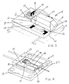
- a fourth submount assembly 10 is illustrated in Figures 5 and 6.
- the fourth submount assembly includes a submount 18 having a first surface 18a which defines a first groove 54 .
- the first groove opens through the first surface and has a bottom 54a and a pair of opposed sidewalls 54b .
- the fourth submount assembly also includes a laser diode 12 mounted upon one sidewall of the first groove.
- the laser diode is generally mounted upon a thermal spreader 25 which, in turn, is mounted to a sidewall of the first groove.
- the laser diode is oriented such that the output of the laser diode is directed toward the opening of the first groove through the first surface of the submount. In the fourth submount assembly illustrated in Figure 6, the output of the laser diode is directed in an upward direction.
- the fourth submount assembly 10 also includes an active gain medium 14 and, more typically, a microresonator cavity 22 including an active gain medium and an associated saturable absorber 24 .
- the microresonator cavity is supported by the first surface 18a of the submount 18 so as to overlie at least that portion of the first groove 54 within which the laser diode 12 is disposed. As such, the output of the laser diode will pump the active gain medium so as to produce a series of laser output pulses.
- the active gain medium can be supported by the first surface of the submount in a variety of fashions, the first surface of the submount in this example preferably defines a plurality of ledges 55 opening into the first groove.
- edge portions of the microresonator cavity can be supported by the plurality of ledges so as to bridge the first groove and overlie the laser diode.
- the first surface of the submount defines ledges adjacent each of the opposed sidewalls 54b of the first groove for supporting the four corners of the microresonator cavity as illustrated in Figures 5 and 6.
- the fourth submount assembly 10 is preferably formed such that the laser diode 12 is appropriately spaced from the microresonator cavity 22 .
- the laser diode is generally spaced from the microresonator cavity by 20 ⁇ 5 microns.
- the laser diode is preferably mounted upon the thermal spreader 25 proximate one end thereof. By appropriately sizing the thermal spreader relative to the depth of the first groove 54 , the laser diode can be appropriately spaced from the microresonator cavity by mounting the thermal spreader to the sidewall of the first groove such that the end of the thermal spreader opposite the laser diode contacts the bottom 54a of the first groove.
- the first surface 18a of the submount 18 also preferably defines a second groove 58 extending between one edge of the submount and the first groove 54.
- the second groove preferably opens into the first groove at a position generally aligned with the laser diode 12 such that the laser diode is exposed via the second groove.
- the first and second grooves are preferably orthogonal.
- the second groove facilitates the mounting of the laser diode upon the sidewall 54b of the first groove by permitting access to the sidewall of the first groove in a direction generally perpendicular to the sidewall.
- the cross-sectional shapes and dimensions of the first and second grooves are generally the same.
- the fourth assembly 10 also generally includes first and second metallization layers 32 , 34 disposed upon different portions of the submount 18 .
- first and second metallization layers can be disposed within respective recesses 20 defined by the first surface 18a of the submount as described above in conjunction with the first submount assembly shown in Fig. 1, the first and second metallization layers of the fourth submount assembly are disposed upon opposite sidewalls 54b of the first groove 54 .
- wire bonds or ball bonds can be established between the laser diode and the metallization layer coating the other sidewall of the first groove.
- the laser diode can be driven so as to produce an output which pumps the microresonator cavity 22 overlying the laser diode.
- the submount 18 in the fourth submount assembly can be mounted upon a heat sink 16 , such as a Peltier heat pump or other thermoelectric cooler.
- the submount is also preferably formed of a thermally conductive, electrically insulating material, such as beryllium oxide, aluminum oxide or aluminum nitride. As such, the submount will provide a path of low thermal impedance from the electro-optic components to the heat sink, while effectively electrically isolating the various electro-optic components as well as the first and second metallization layers.
- the fourth submount assembly 10 can also be mounted within an appropriate electro-optic package 36 , such as a TO-3 or TO-8 package, as shown in Figure 2 and as described below.
- the fourth submount assembly can be packaged as described below in conjunction with Figures 10A-10C so as to further protect the various electro-optic components mounted upon the submount 18 .
- first to third submount assemblies 10 illustrated in Figs. 1-4 and described hereinabove include a submount 18 having a first surface 18a which defines one or more recesses 20 for receiving and aligning respective electro-optic components
- each submount assembly and, more particularly, the submount can define various other types of registration features for aligning respective components.
- a fifth submount assembly includes a submount having a first surface which includes an upper shelf 18c and a lower shelf 18d , wherein the registration feature defined by the submount is an upstanding wall 18e extending between the upper and lower shelves.
- electro-optic components can be precisely positioned with respect to the upstanding wall such that the components are aligned.
- the microresonator cavity 22 and a right angle prism 59 can be mounted upon the lower shelf 18d adjacent the upstanding wall 18e while a laser diode 12 can be mounted upon the upper shelf 18c in alignment with the microresonator cavity such that the output of the laser diode pumps the active gain medium 14 of the microresonator cavity.
- the laser diode is spaced, such as by 20 ⁇ 5 microns, from the registration feature 20 , i.e. the upstanding wall, in order to provide the proper spacing between the emitting facet of the laser diode and the microresonator cavity.
- first and second metallization layers 32 , 34 are also disposed upon different portions of the submount 18 .
- the upper shelf of the submount can define respective recesses within which the first and second metallization layers are disposed, if so desired. Since the submount is not only thermally conductive but is also electrically insulating, the fifth submount assembly 10 can effectively electrically isolate the various electro-optic components and the first and second metallization layers.
- the fifth submount assembly 10 of Figs. 7 and 8 also includes a heat sink 16 , such as a thermoelectric cooler.
- a heat sink 16 such as a thermoelectric cooler.
- conventional thermoelectric coolers include one or more couples, typically formed of bismuth telluride, sandwiched between a pair of thermally conductive plates, such as aluminum oxide plates.
- the submount 18 , in the fifth submount assembly can also serve as the upper plate of the thermoelectric cooler such that the submount and the heat sink 16 are an integral assembly.
- the submount assemblies of Figs. 1-6 (first to fourth submount assemblies) can include other types of heat sinks, including more conventional thermoelectric coolers, if so desired.
- the fifth submount assembly of Figures 7 and 8 can be integrated with a thermoelectric cooler as shown in Figures 1-6, if so desired.
- the submount assembly can be segmented and can correspondingly have a plurality of heat sinks, one of which is associated with each segment of the submount assembly.
- the submount 18 of a sixth submount assembly can be divided into a plurality of segments separated by relatively thin air gaps 19 .
- the submount can include a first segment 18' which supports the laser diode 12 , a second segment 18" which supports the microresonator cavity 22 , and a third segment 18"' which supports the components downstream of the microresonator cavity including the frequency doubling crystal 26 .
- the sixth submount assembly can include three heat sinks and, more preferably, three Peltier heat pumps, one of which is associated with each segment of the submount.
- the sixth submount assembly 10 can include a plurality of temperature sensors 46 , one of which is associated with and monitors the temperature of each respective segment of the submount 18 .
- a controller can receive signals from the temperature sensors that are representative of the temperature of each of the-various segments of the submount. The controller can then apply appropriate voltages to the leads of the Peltier heat pumps in order to individually control the temperature of each segment of the submount.
- the heat pump 16' associated with the first submount segment 18' upon which the laser diode is mounted can cool the first submount segment more than the second and third submount segments.
- the first submount segment is preferably cooled such that the temperature of the laser diode remains relatively constant since the wavelength of the signals emitted by the laser will otherwise vary if the temperature of the laser diode fluctuates.
- the heat pumps associated with the second and third submount segments can cool or heat the respective submount segments such that the microresonator cavity 22 and the other components, such as the frequency doubling crystal 26 , are maintained at a temperature that enhances their operating efficiency.
- the submount assembly including the submount 18 , is initially mounted upon a support surface of a package 36 , such as a TO-3 or TO-8 package.
- a package 36 such as a TO-3 or TO-8 package.
- the heat sink 16 such as a Peltier heat pump, can be initially mounted upon the support surface of the package and the submount can thereafter be mounted upon the heat sink.
- the laser diode 12 and the metallization layers 32 , 34 are generally disposed upon the submount prior to its mounting to the heat sink, one or more of the electro-optic components, including the microresonator cavity 22 , are not mounted upon the submount at the time of its mounting to the heat sink.
- the submount assembly can be mounted in a variety of fashions, the heat sink is typically adhered to the support surface of the package and the second surface 18b of the submount is typically adhered to the heat sink by means of a thermally matched epoxy, such as aluminum oxide filled or silver filled epoxies.
- the package 36 includes a plurality of conductive pins 38 which extend through the base 60 of the package and which surround the support surface of the package.
- the remainder of the electro-optic components can be mounted upon the submount 18 in alignment with the registration features 20 , such as the recesses, defined by the first surface 18a of the submount.
- the microresonator cavity and the right angle prism 59 are preferably mounted upon the submount as described above in conjunction with the firfh submount assembly shown in Figures 7 and 8.
- the electro-optic components of one embodiment are preferably mounted upon the submount by means of a pick and place machine utilizing vacuum pick-up in order to increase the efficiency of the fabrication process.
- the lid 62 is mounted to the base of the package 36 so as to enclose the submount assembly.
- the lid includes a window 64 , however, such that by applying appropriate voltages to the conductive pins 38 , the electro-optic system supported by the submount can emit laser pulses through the window.
- a method embodying the present invention provides a number of advantages.
- a fabrication method embodying the present invention can reduce the handling of the various components, thereby reducing the exposure of the components to static electricity and other deleterious conditions.
- a packaging technique embodying the present invention can limit heating of a number of electro-optic components, including the microresonator cavity, that could deleteriously affect the operation and/or lifetime of the other electro-optic components.
- a submount assembly 10 includes a submount 18 for precisely aligning the various components of an electro-optic system, including a laser diode 12 and an associated microresonator cavity 22 .
- the submount is not only thermally conductive, but is also electrically insulating in order to effectively electrically isolate the various electro-optic components mounted thereupon.
- a packaging method embodying the present invention can reduce handling and heating of the submount assembly following the mounting of the electro-optic components upon the submount, thereby reducing exposure of the various components to heat, static electricity and other deleterious conditions.
Landscapes
- Physics & Mathematics (AREA)
- Electromagnetism (AREA)
- Optics & Photonics (AREA)
- Engineering & Computer Science (AREA)
- Plasma & Fusion (AREA)
- Condensed Matter Physics & Semiconductors (AREA)
- General Physics & Mathematics (AREA)
- Semiconductor Lasers (AREA)
- Die Bonding (AREA)
Applications Claiming Priority (3)
| Application Number | Priority Date | Filing Date | Title |
|---|---|---|---|
| US09/032,457 US6072815A (en) | 1998-02-27 | 1998-02-27 | Microlaser submount assembly and associates packaging method |
| US32457 | 1998-02-27 | ||
| EP99301338A EP0939464B1 (de) | 1998-02-27 | 1999-02-24 | Subträgerbaugruppe und damit verknüpfte Modulpackung |
Related Parent Applications (1)
| Application Number | Title | Priority Date | Filing Date |
|---|---|---|---|
| EP99301338A Division EP0939464B1 (de) | 1998-02-27 | 1999-02-24 | Subträgerbaugruppe und damit verknüpfte Modulpackung |
Publications (3)
| Publication Number | Publication Date |
|---|---|
| EP1365488A2 true EP1365488A2 (de) | 2003-11-26 |
| EP1365488A3 EP1365488A3 (de) | 2004-02-18 |
| EP1365488B1 EP1365488B1 (de) | 2006-06-21 |
Family
ID=21865069
Family Applications (3)
| Application Number | Title | Priority Date | Filing Date |
|---|---|---|---|
| EP03016397A Expired - Lifetime EP1365488B1 (de) | 1998-02-27 | 1999-02-24 | Verfahren zum Verpacken einer Subträgerbaugruppe |
| EP03016396A Expired - Lifetime EP1376787B1 (de) | 1998-02-27 | 1999-02-24 | Subträgerbaugruppe und Verfahren zu dessen Verpackung |
| EP99301338A Expired - Lifetime EP0939464B1 (de) | 1998-02-27 | 1999-02-24 | Subträgerbaugruppe und damit verknüpfte Modulpackung |
Family Applications After (2)
| Application Number | Title | Priority Date | Filing Date |
|---|---|---|---|
| EP03016396A Expired - Lifetime EP1376787B1 (de) | 1998-02-27 | 1999-02-24 | Subträgerbaugruppe und Verfahren zu dessen Verpackung |
| EP99301338A Expired - Lifetime EP0939464B1 (de) | 1998-02-27 | 1999-02-24 | Subträgerbaugruppe und damit verknüpfte Modulpackung |
Country Status (4)
| Country | Link |
|---|---|
| US (1) | US6072815A (de) |
| EP (3) | EP1365488B1 (de) |
| JP (1) | JPH11330627A (de) |
| DE (3) | DE69925524T2 (de) |
Families Citing this family (39)
| Publication number | Priority date | Publication date | Assignee | Title |
|---|---|---|---|---|
| US6240113B1 (en) * | 1998-02-27 | 2001-05-29 | Litton Systems, Inc. | Microlaser-based electro-optic system and associated fabrication method |
| JP3211770B2 (ja) * | 1998-05-11 | 2001-09-25 | 日本電気株式会社 | 固体レーザ装置及びそれを備えた固体レーザ増幅器 |
| US6534794B1 (en) | 1999-08-05 | 2003-03-18 | Matsushita Electric Industrial Co., Ltd. | Semiconductor light-emitting unit, optical apparatus and optical disk system having heat sinking means and a heating element incorporated with the mounting system |
| US6501772B1 (en) | 2000-08-11 | 2002-12-31 | Litton Systems, Inc. | Microlaser assembly having a microresonator and aligned electro-optic components |
| CA2354897A1 (en) | 2000-08-11 | 2002-02-11 | Litton Systems, Inc. | Wedge-shaped microresonator and associated microlaser assembly |
| DE60234823D1 (de) * | 2001-04-04 | 2010-02-04 | Coherent Deos | Gütegeschalteter co2 laser für materialbearbeitung |
| US20020167976A1 (en) * | 2001-04-04 | 2002-11-14 | Seguin Vernon A. | Thermally efficient laser head |
| US6697408B2 (en) * | 2001-04-04 | 2004-02-24 | Coherent, Inc. | Q-switched cavity dumped CO2 laser for material processing |
| US6870866B2 (en) * | 2001-06-05 | 2005-03-22 | Axcel Photonics, Inc. | Powerpack laser diode assemblies |
| WO2003012938A1 (en) * | 2001-07-27 | 2003-02-13 | General Instrument Corporation | Inexpensive analog laser module |
| WO2003015227A1 (en) * | 2001-07-27 | 2003-02-20 | General Instrument Corporation | Method and apparatus for monitoring and maintaining the temperature of an analog laser module |
| US6868104B2 (en) * | 2001-09-06 | 2005-03-15 | Finisar Corporation | Compact laser package with integrated temperature control |
| US6818464B2 (en) * | 2001-10-17 | 2004-11-16 | Hymite A/S | Double-sided etching technique for providing a semiconductor structure with through-holes, and a feed-through metalization process for sealing the through-holes |
| KR100400081B1 (ko) * | 2001-11-24 | 2003-09-29 | 한국전자통신연구원 | 광전 모듈용 서브마운트 및 이를 이용한 실장 방법 |
| US6724791B1 (en) * | 2002-07-02 | 2004-04-20 | C-Cor.Net Corp. | Method and apparatus for controlling the temperature of a laser module in fiber optic transmissions |
| US6891879B2 (en) | 2002-09-23 | 2005-05-10 | Litton Systems, Inc. | Microlaser cavity assembly and associated packaging method |
| US7039079B2 (en) * | 2003-03-14 | 2006-05-02 | Coherent, Inc. | Pulsed CO2 laser including an optical damage resistant electro-optical switching arrangement |
| WO2005030980A2 (en) * | 2003-09-22 | 2005-04-07 | Snake Creek Lasers Llc | High densiity methods for producing diode-pumped micro lasers |
| US7681306B2 (en) * | 2004-04-28 | 2010-03-23 | Hymite A/S | Method of forming an assembly to house one or more micro components |
| KR100565077B1 (ko) * | 2004-08-05 | 2006-03-30 | 삼성전자주식회사 | 히트 싱크를 가진 광학 헤드 |
| DE102004057454B4 (de) * | 2004-11-25 | 2009-10-22 | Jenoptik Laserdiode Gmbh | Diodenlasermodul und Verfahren zu dessen Herstellung |
| JP2007059692A (ja) * | 2005-08-25 | 2007-03-08 | Sumitomo Electric Ind Ltd | 光モジュール |
| DE102006017293A1 (de) * | 2005-12-30 | 2007-07-05 | Osram Opto Semiconductors Gmbh | Verfahren zur Herstellung einer optisch pumpbaren Halbleitervorrichtung |
| US7515346B2 (en) * | 2006-07-18 | 2009-04-07 | Coherent, Inc. | High power and high brightness diode-laser array for material processing applications |
| US7394841B1 (en) * | 2007-01-18 | 2008-07-01 | Epicrystals Oy | Light emitting device for visual applications |
| JP4277908B2 (ja) * | 2007-02-06 | 2009-06-10 | セイコーエプソン株式会社 | 光源装置、照明装置、モニタ装置及びプロジェクタ |
| US7660500B2 (en) * | 2007-05-22 | 2010-02-09 | Epicrystals Oy | Light emitting array |
| WO2009081470A1 (ja) * | 2007-12-21 | 2009-07-02 | Mitsubishi Electric Corporation | レーザ光源モジュール |
| DE102007062047A1 (de) * | 2007-12-21 | 2009-07-16 | Osram Opto Semiconductors Gmbh | Kompaktgehäuse |
| JP5082862B2 (ja) * | 2008-01-09 | 2012-11-28 | セイコーエプソン株式会社 | 光源装置、照明装置及び画像表示装置 |
| JP2009192873A (ja) * | 2008-02-15 | 2009-08-27 | Seiko Epson Corp | 光源装置、画像表示装置及びモニタ装置 |
| EP2256877B1 (de) * | 2008-03-18 | 2013-01-09 | Mitsubishi Electric Corporation | Optisches modul |
| US7756175B2 (en) * | 2008-10-30 | 2010-07-13 | The United States Of America As Represented By The Secretary Of The Army | Pumped semiconductor laser systems and methods |
| JP4980454B2 (ja) * | 2010-09-10 | 2012-07-18 | パナソニック株式会社 | レーザ光源装置 |
| CN102570293A (zh) * | 2012-02-13 | 2012-07-11 | 苏州华必大激光有限公司 | 高热负载大功率半导体激光器 |
| JP6097253B2 (ja) * | 2014-07-02 | 2017-03-15 | 住友電気工業株式会社 | 三色光光源 |
| USD749713S1 (en) * | 2014-07-31 | 2016-02-16 | Innovative Medical Equipment, Llc | Heat exchanger |
| DE102018106504B4 (de) * | 2018-03-20 | 2020-03-12 | Schott Ag | Anordnung mit einem TO-Gehäuse, Verfahren zu dessen Herstellung sowie optisches Datenübertragungssystem |
| CN113140948B (zh) * | 2020-01-17 | 2022-09-06 | 福州市众心联光电科技有限公司 | 一种光学晶体支架的制作方法 |
Family Cites Families (47)
| Publication number | Priority date | Publication date | Assignee | Title |
|---|---|---|---|---|
| US4012833A (en) * | 1973-12-28 | 1977-03-22 | Sony Corporation | Method of making display structure having light emitting diodes |
| DE2737345C2 (de) * | 1976-08-20 | 1991-07-25 | Canon K.K., Tokio/Tokyo | Halbleiterlaser-Vorrichtung mit einem Peltier-Element |
| FR2426347A1 (fr) * | 1978-05-18 | 1979-12-14 | Thomson Csf | Source laser a semi-conducteur et son procede de fabrication |
| JPS577989A (en) * | 1980-06-17 | 1982-01-16 | Matsushita Electric Ind Co Ltd | Mount for semiconductor laser |
| US4550333A (en) * | 1983-09-13 | 1985-10-29 | Xerox Corporation | Light emitting semiconductor mount |
| GB2189620B (en) * | 1986-04-23 | 1990-03-28 | Stc Plc | Optical fibre transmission package |
| DE3531734A1 (de) * | 1985-09-05 | 1987-03-12 | Siemens Ag | Einrichtung zur positionierung eines halbleiterlasers mit selbstjustierender wirkung fuer eine anzukoppelnde glasfaser |
| FR2600055B1 (fr) * | 1986-06-16 | 1988-08-26 | Commissariat Energie Atomique | Aluminates mixtes de lanthanide-magnesium, lasers utilisant des monocristaux de ces aluminates |
| US4731795A (en) * | 1986-06-26 | 1988-03-15 | Amoco Corporation | Solid state laser |
| GB8712808D0 (en) * | 1987-06-01 | 1987-07-08 | Bt & D Technologies Ltd | Optical transmitters |
| US4860304A (en) * | 1988-02-02 | 1989-08-22 | Massachusetts Institute Of Technology | Solid state microlaser |
| US5256164A (en) * | 1988-02-02 | 1993-10-26 | Massachusetts Institute Of Technology | Method of fabricating a microchip laser |
| US5265116A (en) * | 1988-02-02 | 1993-11-23 | Massachusetts Institute Of Technology | Microchip laser |
| US5115445A (en) * | 1988-02-02 | 1992-05-19 | Massachusetts Institute Of Technology | Microchip laser array |
| US4953166A (en) * | 1988-02-02 | 1990-08-28 | Massachusetts Institute Of Technology | Microchip laser |
| US4904036A (en) * | 1988-03-03 | 1990-02-27 | American Telephone And Telegraph Company, At&T Bell Laboratories | Subassemblies for optoelectronic hybrid integrated circuits |
| US4897711A (en) * | 1988-03-03 | 1990-01-30 | American Telephone And Telegraph Company | Subassembly for optoelectronic devices |
| US4805177A (en) * | 1988-04-25 | 1989-02-14 | Laser Diode Products, Inc. | Laser construction |
| US5233580A (en) * | 1988-12-19 | 1993-08-03 | Rohm Co., Ltd. | Laser diode unit welded to a mounting member by laser light |
| US5029335A (en) * | 1989-02-21 | 1991-07-02 | Amoco Corporation | Heat dissipating device for laser diodes |
| DE3925201A1 (de) * | 1989-07-29 | 1991-02-07 | Messerschmitt Boelkow Blohm | Optische bank zur halterung optischer, elektrischer u.a. komponenten |
| US5026138A (en) * | 1989-08-29 | 1991-06-25 | Gte Laboratories Incorporated | Multi-fiber alignment package for tilted facet optoelectronic components |
| US5156999A (en) * | 1990-06-08 | 1992-10-20 | Wai-Hon Lee | Packaging method for semiconductor laser/detector devices |
| US5113404A (en) * | 1990-07-05 | 1992-05-12 | At&T Bell Laboratories | Silicon-based optical subassembly |
| US5264392A (en) * | 1990-07-05 | 1993-11-23 | At&T Bell Laboratories | Fabrication technique for silicon-based optical subassemblies |
| US5124281A (en) * | 1990-08-27 | 1992-06-23 | At&T Bell Laboratories | Method of fabricating a photonics module comprising a spherical lens |
| DE4041130A1 (de) * | 1990-12-21 | 1992-07-02 | Messerschmitt Boelkow Blohm | Festkoerper-lasersystem |
| US5128951A (en) * | 1991-03-04 | 1992-07-07 | Karpinski Arthur A | Laser diode array and method of fabrication thereof |
| US5181214A (en) * | 1991-11-18 | 1993-01-19 | Harmonic Lightwaves, Inc. | Temperature stable solid-state laser package |
| FR2683948B1 (fr) * | 1991-11-20 | 1994-03-04 | France Telecom | Structure de composant optique integre contenant une terre rare, procede de realisation et applications. |
| US5295146A (en) * | 1992-04-10 | 1994-03-15 | Polaroid Corporation | Solid state gain mediums for optically pumped monolithic laser |
| JPH06132613A (ja) * | 1992-10-14 | 1994-05-13 | Fujitsu Ltd | 半導体レーザ装置 |
| JPH06232504A (ja) * | 1993-01-29 | 1994-08-19 | Canon Inc | レーザ走査装置 |
| JP2842132B2 (ja) * | 1993-03-05 | 1998-12-24 | 松下電器産業株式会社 | 光学デバイス |
| US5357536A (en) * | 1993-05-07 | 1994-10-18 | Xerox Corporation | Method and apparatus for the positioning of laser diodes |
| ATE193166T1 (de) * | 1993-08-26 | 2000-06-15 | Laser Power Corp | Tiefblauer mikrolaser |
| FR2712743B1 (fr) * | 1993-11-15 | 1995-12-15 | Commissariat Energie Atomique | Cavité laser à déclenchement passif par absorbant saturable et laser incorporant cette cavité. |
| FR2712742B1 (fr) * | 1993-11-15 | 1995-12-15 | Commissariat Energie Atomique | Microlaser solide, monolithique, autoaligné, à déclenchement passif par absorbant saturable et son procédé de fabrication. |
| US5394413A (en) * | 1994-02-08 | 1995-02-28 | Massachusetts Institute Of Technology | Passively Q-switched picosecond microlaser |
| JP3324286B2 (ja) * | 1994-06-29 | 2002-09-17 | 住友電気工業株式会社 | アナログpdモジュール及びその製造方法 |
| US5521936A (en) * | 1995-02-01 | 1996-05-28 | Paradigm Lasers, Inc. | Radial laser diode array |
| FR2734092B1 (fr) * | 1995-05-12 | 1997-06-06 | Commissariat Energie Atomique | Microlaser monolithique declenche et materiau non lineaire intracavite |
| FR2734096B1 (fr) * | 1995-05-12 | 1997-06-06 | Commissariat Energie Atomique | Cavite microlaser et microlaser solide impulsionnel a declenchement passif et a commande externe |
| FR2734094B1 (fr) * | 1995-05-12 | 1997-06-06 | Commissariat Energie Atomique | Emetteur infrarouge monolithique a semi-conducteur pompe par un microlaser solide declenche |
| FR2736217B1 (fr) * | 1995-06-27 | 1997-08-08 | Commissariat Energie Atomique | Cavite microlaser et microlaser solide impulsionnel a declenchement actif par micromodulateur |
| JPH09293917A (ja) * | 1996-04-26 | 1997-11-11 | Mitsui Petrochem Ind Ltd | 半導体レーザ励起固体レーザ装置 |
| US5828683A (en) * | 1997-04-21 | 1998-10-27 | The Regents Of The University Of California | High density, optically corrected, micro-channel cooled, v-groove monolithic laser diode array |
-
1998
- 1998-02-27 US US09/032,457 patent/US6072815A/en not_active Expired - Fee Related
-
1999
- 1999-02-24 EP EP03016397A patent/EP1365488B1/de not_active Expired - Lifetime
- 1999-02-24 DE DE69925524T patent/DE69925524T2/de not_active Expired - Fee Related
- 1999-02-24 EP EP03016396A patent/EP1376787B1/de not_active Expired - Lifetime
- 1999-02-24 DE DE69932105T patent/DE69932105T2/de not_active Expired - Fee Related
- 1999-02-24 DE DE69931530T patent/DE69931530T2/de not_active Expired - Fee Related
- 1999-02-24 EP EP99301338A patent/EP0939464B1/de not_active Expired - Lifetime
- 1999-02-26 JP JP11049610A patent/JPH11330627A/ja active Pending
Also Published As
| Publication number | Publication date |
|---|---|
| DE69931530D1 (de) | 2006-06-29 |
| DE69932105D1 (de) | 2006-08-03 |
| US6072815A (en) | 2000-06-06 |
| DE69932105T2 (de) | 2007-04-26 |
| DE69925524D1 (de) | 2005-07-07 |
| DE69925524T2 (de) | 2006-01-26 |
| EP1376787B1 (de) | 2006-05-24 |
| EP1376787A2 (de) | 2004-01-02 |
| JPH11330627A (ja) | 1999-11-30 |
| EP0939464A2 (de) | 1999-09-01 |
| EP1365488B1 (de) | 2006-06-21 |
| EP1365488A3 (de) | 2004-02-18 |
| DE69931530T2 (de) | 2006-12-21 |
| EP0939464A3 (de) | 2002-01-02 |
| EP0939464B1 (de) | 2005-06-01 |
| EP1376787A3 (de) | 2004-05-06 |
Similar Documents
| Publication | Publication Date | Title |
|---|---|---|
| EP1365488B1 (de) | Verfahren zum Verpacken einer Subträgerbaugruppe | |
| US7060515B2 (en) | Method of manufacturing a laser diode package | |
| EP1079480B1 (de) | Elektrooptische Systeme | |
| US5325384A (en) | Structure and method for mounting laser diode arrays | |
| US6826916B2 (en) | Laser module, Peltier module, and Peltier module integrated heat spreader | |
| US5140607A (en) | Side-pumped laser with angled diode pumps | |
| US5561684A (en) | Laser diode pumped solid state laser construction | |
| JP2000156538A (ja) | 温度制御されたマイクロチップレ―ザアセンブリ及び関連するサブマウントアセンブリ | |
| CN110574176A (zh) | 具有iii–v族增益材料和集成散热器的电光器件 | |
| US6449296B1 (en) | Semiconductor laser device | |
| US8518814B2 (en) | Methods of fabrication of high-density laser diode stacks | |
| WO1994015386A1 (en) | Multi-element optically pumped external cavity laser system | |
| WO2024155585A1 (en) | Systems and methods for cooling high power devices | |
| US6967982B2 (en) | Semiconductor laser device with a strain reduction cushion function, semiconductor laser module, and semiconductor laser device fabrication method | |
| Demaria et al. | Design of highly efficient high-power optically pumped semiconductor disk lasers | |
| US20240055835A1 (en) | Red green blue laser module | |
| US20040026779A1 (en) | Semiconductor devices with improved heat dissipation and method for fabricating same | |
| JPH0567844A (ja) | 半導体レーザモジユール | |
| US6724784B2 (en) | Optical wavelength locker module having a high thermal conductive material | |
| EP4434310B1 (de) | Terahertz-gunn-oszillator unter verwendung von galliumnitrid | |
| EP1079484A2 (de) | Halbleiterlaservorrichtung, Halbleiterlasermodul und Fasermodul | |
| US20070085081A1 (en) | Thermally efficient semiconductor laser structure and method of forming same | |
| RU2153745C1 (ru) | Полупроводниковый лазер | |
| JP2001160648A (ja) | 半導体レーザ装置 |
Legal Events
| Date | Code | Title | Description |
|---|---|---|---|
| PUAI | Public reference made under article 153(3) epc to a published international application that has entered the european phase |
Free format text: ORIGINAL CODE: 0009012 |
|
| AC | Divisional application: reference to earlier application |
Ref document number: 0939464 Country of ref document: EP Kind code of ref document: P |
|
| AK | Designated contracting states |
Kind code of ref document: A2 Designated state(s): CH DE FR GB IT LI |
|
| PUAL | Search report despatched |
Free format text: ORIGINAL CODE: 0009013 |
|
| AK | Designated contracting states |
Kind code of ref document: A3 Designated state(s): CH DE FR GB IT LI |
|
| RIC1 | Information provided on ipc code assigned before grant |
Ipc: 7H 01S 5/022 B Ipc: 7H 01S 3/02 B Ipc: 7H 01S 3/067 A Ipc: 7H 01L 25/16 B Ipc: 7G 02B 6/42 B Ipc: 7H 01S 5/02 B |
|
| 17P | Request for examination filed |
Effective date: 20040816 |
|
| AKX | Designation fees paid |
Designated state(s): CH DE FR GB IT LI |
|
| 17Q | First examination report despatched |
Effective date: 20050504 |
|
| GRAP | Despatch of communication of intention to grant a patent |
Free format text: ORIGINAL CODE: EPIDOSNIGR1 |
|
| GRAS | Grant fee paid |
Free format text: ORIGINAL CODE: EPIDOSNIGR3 |
|
| GRAA | (expected) grant |
Free format text: ORIGINAL CODE: 0009210 |
|
| AC | Divisional application: reference to earlier application |
Ref document number: 0939464 Country of ref document: EP Kind code of ref document: P |
|
| AK | Designated contracting states |
Kind code of ref document: B1 Designated state(s): CH DE FR GB IT LI |
|
| PG25 | Lapsed in a contracting state [announced via postgrant information from national office to epo] |
Ref country code: IT Free format text: LAPSE BECAUSE OF FAILURE TO SUBMIT A TRANSLATION OF THE DESCRIPTION OR TO PAY THE FEE WITHIN THE PRESCRIBED TIME-LIMIT;WARNING: LAPSES OF ITALIAN PATENTS WITH EFFECTIVE DATE BEFORE 2007 MAY HAVE OCCURRED AT ANY TIME BEFORE 2007. THE CORRECT EFFECTIVE DATE MAY BE DIFFERENT FROM THE ONE RECORDED. Effective date: 20060621 Ref country code: LI Free format text: LAPSE BECAUSE OF FAILURE TO SUBMIT A TRANSLATION OF THE DESCRIPTION OR TO PAY THE FEE WITHIN THE PRESCRIBED TIME-LIMIT Effective date: 20060621 Ref country code: CH Free format text: LAPSE BECAUSE OF FAILURE TO SUBMIT A TRANSLATION OF THE DESCRIPTION OR TO PAY THE FEE WITHIN THE PRESCRIBED TIME-LIMIT Effective date: 20060621 |
|
| REG | Reference to a national code |
Ref country code: GB Ref legal event code: FG4D |
|
| REG | Reference to a national code |
Ref country code: CH Ref legal event code: EP |
|
| REF | Corresponds to: |
Ref document number: 69932105 Country of ref document: DE Date of ref document: 20060803 Kind code of ref document: P |
|
| REG | Reference to a national code |
Ref country code: CH Ref legal event code: PL |
|
| ET | Fr: translation filed | ||
| PLBE | No opposition filed within time limit |
Free format text: ORIGINAL CODE: 0009261 |
|
| STAA | Information on the status of an ep patent application or granted ep patent |
Free format text: STATUS: NO OPPOSITION FILED WITHIN TIME LIMIT |
|
| 26N | No opposition filed |
Effective date: 20070322 |
|
| GBPC | Gb: european patent ceased through non-payment of renewal fee |
Effective date: 20070224 |
|
| REG | Reference to a national code |
Ref country code: FR Ref legal event code: ST Effective date: 20071030 |
|
| PG25 | Lapsed in a contracting state [announced via postgrant information from national office to epo] |
Ref country code: FR Free format text: LAPSE BECAUSE OF NON-PAYMENT OF DUE FEES Effective date: 20070228 Ref country code: GB Free format text: LAPSE BECAUSE OF NON-PAYMENT OF DUE FEES Effective date: 20070224 |
|
| PGFP | Annual fee paid to national office [announced via postgrant information from national office to epo] |
Ref country code: DE Payment date: 20080219 Year of fee payment: 10 |
|
| PG25 | Lapsed in a contracting state [announced via postgrant information from national office to epo] |
Ref country code: DE Free format text: LAPSE BECAUSE OF NON-PAYMENT OF DUE FEES Effective date: 20090901 |