EP1367151A1 - Einkristalline ferromagnetische verbindung auf gruppe-ii-vi- oder gruppe-iii-v-basis und verfahren zur einstellung ihrer ferromagnetischen eigenschaften - Google Patents
Einkristalline ferromagnetische verbindung auf gruppe-ii-vi- oder gruppe-iii-v-basis und verfahren zur einstellung ihrer ferromagnetischen eigenschaften Download PDFInfo
- Publication number
- EP1367151A1 EP1367151A1 EP02701657A EP02701657A EP1367151A1 EP 1367151 A1 EP1367151 A1 EP 1367151A1 EP 02701657 A EP02701657 A EP 02701657A EP 02701657 A EP02701657 A EP 02701657A EP 1367151 A1 EP1367151 A1 EP 1367151A1
- Authority
- EP
- European Patent Office
- Prior art keywords
- group
- ferromagnetic
- transition metal
- compound
- crystal
- Prior art date
- Legal status (The legal status is an assumption and is not a legal conclusion. Google has not performed a legal analysis and makes no representation as to the accuracy of the status listed.)
- Withdrawn
Links
Images





Classifications
-
- C—CHEMISTRY; METALLURGY
- C30—CRYSTAL GROWTH
- C30B—SINGLE-CRYSTAL GROWTH; UNIDIRECTIONAL SOLIDIFICATION OF EUTECTIC MATERIAL OR UNIDIRECTIONAL DEMIXING OF EUTECTOID MATERIAL; REFINING BY ZONE-MELTING OF MATERIAL; PRODUCTION OF A HOMOGENEOUS POLYCRYSTALLINE MATERIAL WITH DEFINED STRUCTURE; SINGLE CRYSTALS OR HOMOGENEOUS POLYCRYSTALLINE MATERIAL WITH DEFINED STRUCTURE; AFTER-TREATMENT OF SINGLE CRYSTALS OR A HOMOGENEOUS POLYCRYSTALLINE MATERIAL WITH DEFINED STRUCTURE; APPARATUS THEREFOR
- C30B29/00—Single crystals or homogeneous polycrystalline material with defined structure characterised by the material or by their shape
- C30B29/10—Inorganic compounds or compositions
- C30B29/46—Sulfur-, selenium- or tellurium-containing compounds
- C30B29/48—AIIBVI compounds wherein A is Zn, Cd or Hg, and B is S, Se or Te
-
- C—CHEMISTRY; METALLURGY
- C30—CRYSTAL GROWTH
- C30B—SINGLE-CRYSTAL GROWTH; UNIDIRECTIONAL SOLIDIFICATION OF EUTECTIC MATERIAL OR UNIDIRECTIONAL DEMIXING OF EUTECTOID MATERIAL; REFINING BY ZONE-MELTING OF MATERIAL; PRODUCTION OF A HOMOGENEOUS POLYCRYSTALLINE MATERIAL WITH DEFINED STRUCTURE; SINGLE CRYSTALS OR HOMOGENEOUS POLYCRYSTALLINE MATERIAL WITH DEFINED STRUCTURE; AFTER-TREATMENT OF SINGLE CRYSTALS OR A HOMOGENEOUS POLYCRYSTALLINE MATERIAL WITH DEFINED STRUCTURE; APPARATUS THEREFOR
- C30B23/00—Single-crystal growth by condensing evaporated or sublimed materials
- C30B23/002—Controlling or regulating
-
- C—CHEMISTRY; METALLURGY
- C30—CRYSTAL GROWTH
- C30B—SINGLE-CRYSTAL GROWTH; UNIDIRECTIONAL SOLIDIFICATION OF EUTECTIC MATERIAL OR UNIDIRECTIONAL DEMIXING OF EUTECTOID MATERIAL; REFINING BY ZONE-MELTING OF MATERIAL; PRODUCTION OF A HOMOGENEOUS POLYCRYSTALLINE MATERIAL WITH DEFINED STRUCTURE; SINGLE CRYSTALS OR HOMOGENEOUS POLYCRYSTALLINE MATERIAL WITH DEFINED STRUCTURE; AFTER-TREATMENT OF SINGLE CRYSTALS OR A HOMOGENEOUS POLYCRYSTALLINE MATERIAL WITH DEFINED STRUCTURE; APPARATUS THEREFOR
- C30B29/00—Single crystals or homogeneous polycrystalline material with defined structure characterised by the material or by their shape
- C30B29/10—Inorganic compounds or compositions
- C30B29/40—AIIIBV compounds wherein A is B, Al, Ga, In or Tl and B is N, P, As, Sb or Bi
- C30B29/403—AIII-nitrides
-
- C—CHEMISTRY; METALLURGY
- C30—CRYSTAL GROWTH
- C30B—SINGLE-CRYSTAL GROWTH; UNIDIRECTIONAL SOLIDIFICATION OF EUTECTIC MATERIAL OR UNIDIRECTIONAL DEMIXING OF EUTECTOID MATERIAL; REFINING BY ZONE-MELTING OF MATERIAL; PRODUCTION OF A HOMOGENEOUS POLYCRYSTALLINE MATERIAL WITH DEFINED STRUCTURE; SINGLE CRYSTALS OR HOMOGENEOUS POLYCRYSTALLINE MATERIAL WITH DEFINED STRUCTURE; AFTER-TREATMENT OF SINGLE CRYSTALS OR A HOMOGENEOUS POLYCRYSTALLINE MATERIAL WITH DEFINED STRUCTURE; APPARATUS THEREFOR
- C30B29/00—Single crystals or homogeneous polycrystalline material with defined structure characterised by the material or by their shape
- C30B29/10—Inorganic compounds or compositions
- C30B29/40—AIIIBV compounds wherein A is B, Al, Ga, In or Tl and B is N, P, As, Sb or Bi
- C30B29/403—AIII-nitrides
- C30B29/406—Gallium nitride
Definitions
- the present invention relates to a single-crystal ferromagnetic material which is achieved by giving ferromagnetic characteristics to Group II-VI or III-V compounds allowing light to be transmitted therethrough.
- Eg bandgap
- a Group III-V compound selected from the group consisting of GaAs, InAs, InP and GaP has a property allowing transmission of light ranging from the red to ultraviolet wavelength.
- a material with ferromagnetism having a high ferromagnetic transition temperature is obtained using this compound, it can also contribute to a major breakthrough in preparing optical devices such as an optical quantum computer utilizing coherent spin dynamics.
- Eg bandgap
- the obtained material can be widely used for the development of magnetooptic-spin devices utilizing a magnetooptic effect, for example, by combining it with a light-emitting element, such as a semiconductor laser, made of a Group II-VI or III-V compound with excitons having a high binding energy, or arranging it to generate circularly-polarized light depending on its magnetic state.
- a light-emitting element such as a semiconductor laser
- a Group II-VI or III-V compound with excitons having a high binding energy or arranging it to generate circularly-polarized light depending on its magnetic state.
- the above material When the above material is used to provide a ferromagnetic-memory in such a manner that light is irradiated thereon to change its magnetization state, it should be prepared to have desired ferromagnetic characteristics, for example, to have a ferromagnetic transition temperature (Currie temperature) arranged at a value (a temperature slightly higher that room temperature) allowing the magnetization state to be changed in response to the light irradiation.
- a ferromagnetic transition temperature (Currie temperature) arranged at a value (a temperature slightly higher that room temperature) allowing the magnetization state to be changed in response to the light irradiation.
- a transition metal element such as Ti, V, Cr, Mn, Fe, Co, Ni, Cu, Rh or Ru
- a Group II-VI compound can be adequately formed as a single crystal even if about 50 at % of Zn or Cd in the Group II-VI compound is substituted with the transition metal element, and particularly that the single crystal can be formed in a stable ferromagnetic state by adding either one of transition metal elements V and Cr to a Group II-VI compound to form a mixed crystal, so as to allow d-electrons or d-holes to wander about the crystal, or by additionally doping a carrier into a Group II-VI compound.
- a transition metal element such as Ti, V, Cr, Mn, Fe, Co, Ni, Cu, Rh or Ru, has an ion radius close to that of Ga or In, and thus the Group III-V non-nitride can be adequately formed as a single crystal even if about 25 at % of Ga or In in the Group III-V non-nitride is substituted with the transition metal element; that a single crystal with ferromagnetism can be obtained by adding Mn to the Group II-VI non-nitride semiconductor to form a mixed crystal, which can dope holes more than the electron state of Mn (five d-electrons); and that an effect
- the inventers verified that the single crystal can be obtained in a stable ferromagnetic state having a drastically higher Currie point than that from the conventional Mn doping, only by adding the transition metal element, such as V or Cr, to the Group III-V non-nitride, so as to form a mixed crystal of the transition metal element with the Group III-V non-nitride.
- the transition metal element such as V or Cr
- the inventors found: that the Group III-V nitride can be adequately formed as a single crystal even if about 25 at % of Ga or Al in the Group III-V nitride is substituted (mixed-crystallized) with a transition metal element, such as V, Cr or Mn, at a low temperature through a non-equilibrium crystal growth method; that a single crystal with ferromagnetism can be obtained by adding V, Cr or Mn to the Group III-V nitride semiconductor to form a mixed crystal, so as to dope holes or electrons (increase/reduce electrons) depending on change in the electron state of V, Cr or Mn; and that an effect equivalent to that from the addition of holes to d-electrons can be obtained by adding the transition metal element, such as V, Cr or Mn,
- the inventers verified that the single crystal can be obtained in a stable ferromagnetic state by adding the transition metal element, such as V, Cr or Mn, to the Group III-V nitride, so as to form a mixed crystal of the transition metal element with the Group III-V nitride.
- the transition metal element such as V, Cr or Mn
- the Group III-V compound-based single-crystal ferromagnetic material can be obtained with different ferromagnetic transition temperatures, or in a stabilized ferromagnetic state more than an antiferromagnetic or paramagnetic state, or with an adjustable energy in the ferromagnetic state (for example, an energy such that while an antiferromagnetic state is caused by a narrow margin, it can normally maintain the ferromagnetic state), by changing the concentration of transition metal elements, or forming a mixed crystal with two or more kinds of the transition metal elements in combination or with different ratios of these transition metal elements, or additionally adding n-type and/or p-type dopants; and that the Group III-V compound-based single-crystal ferromagnetic material can have a desired filter function by selectively adding two or more kinds of the transition metal elements to form a mixed crystal, because each of the transition metal elements has a different minimum transmittable wavelength.
- an adjustable energy in the ferromagnetic state for example, an energy such that while an antiferrom
- a method of adjusting the ferromagnetic characteristic of a Group II-VI or III-V compound-based single-crystal ferromagnetic material comprising:
- the present invention also provides a method of adjusting the ferromagnetic characteristic of a Group II-VI or III-V compound-based single-crystal ferromagnetic material, comprising:
- a method of adjusting the ferromagnetic characteristic of a Group III-V compound-based single-crystal ferromagnetic material comprising:
- the present invention also provides a method of adjusting the ferromagnetic characteristic of a Group III-V compound-based single-crystal ferromagnetic material, comprising:
- Each of the above methods may includes forming a mixed crystal of the transition metal elements set forth in (2), to adjust the energy of a ferromagnetic state, and to reduce the entire energy by the kinetic energy of holes or electrons introduced from the metal elements themselves, so as to stabilize the ferromagnetic state.
- Each of the above methods may also includes forming a mixed crystal of the transition metal elements set forth in (2), to control the magnitude and sign of the magnetic interaction between the metal atoms by holes or electrons introduced from the metal elements themselves, so as to stabilize a ferromagnetic state.
- each of the above methods may includes forming a mixed crystal of the transition metal elements set forth in (2), to control the magnitude and sign of the magnetic interaction between the metal atoms by holes or electrons introduced from the metal elements themselves, and control a light-transmission characteristic based on the mixed crystal of the metal elements so as to provide a desired optical filter characteristic to the material.
- the dopant will enters in the matrix of the Group II-VI compound or the Group III-V compound.
- the dopant acts on d-electrodes close to the Group II-VI compound or the Group III-V compound to vary holes or electrons so as to allow the ferromagnetic characteristics to be adjusted.
- a Group II-VI compound-based ferromagnetic material at least one transition metal element selected from the group consisting of V and Cr is substituted for the Group II element of a Group II-VI compound to form a mixed crystal.
- the Group II-VI compound herein means a chalcogen compound including Zn and Cd, and specifically includes ZnS, ZnSe, ZnTe, CdS, CdSe and CdTe.
- the aforementioned transition metal element has an ion radius close to that of a Group II element such as Zn or Cd.
- the inventors have made various researches for obtaining a ferromagnetic material using a Group II-VI compound.
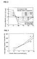
- the transition metal element V or Cr allows d-electrons to be released therefrom more than Mn exhibiting anti-ferromagnetism by three, and thus, as seen from FIG. 2 showing the difference ⁇ E between the entire energy of an antiferromagnetic spin glass state and the entire energy of a ferromagnetic state in ZnTe, the mixed crystal can exhibit ferromagnetism only by crystallizing V or Cr in the Group II-VI compound independently.
- FIG. 2 shows examples in which the mixed ratio of the crystallized transition metal element to Zn of ZnTe is arranged at 5, 10, 15, 20 and 25 at %.
- the mixed crystal exhibits ferromagnetism even at the mixed ratio of several %, and the crystallization and transparency are not degraded even if the ratio is increased.
- the mixed ratio is can be set in the range of 1 to 99 at %, preferably 5 to 80 at % to provide sufficient ferromagnetism.
- the kind of the transition metal element is not limited to one, but two or more kinds of transition metal elements may be crystallized together as described later.
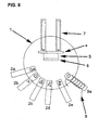
- a thin film of the Zn compound containing the above transition metal element can be formed, for example, by using an MBE apparatus as schematically shown in FIG 1.
- a substrate 5, such as GaN or sapphire, for growing a ZnTe compound is placed on a substrate holder 4 contained in a chamber 1 capable of maintaining a ultra-high-vacuum of about 1.33 ⁇ 10 -6 Pa, and a heater 7 is operable to heat the substrate 5.
- the MBE apparatus includes: a cell 2a disposed opposed to the substrate 5 held by the substrate holder 4, and containing Zn as a material (source) of an element constituting a compound to be grown; a cell 2d containing Te; a cell 2b (while Fig. 1 shows only one cell, two or more cells will be provided if two or more transition metal elements are crystallized together) containing a transition metal element such as V or Cr; a cell 2c containing an n-type dopant such as Ga, Al, In, Cl or Br; and an RF radical cell 3a for generating a radical nitrogen N as a p-type dopant.
- the solid material such as Zn or transition metal may be contained in a cell in the form of its metal oxide, and heated into an atomic form.
- RF radio frequency wave
- Each of the materials of Zn, transition metal element and n-type dopant is prepared by atomizing a solid source having a purity of 99.99999 %.
- N+ or N 2 in an excited state is prepared by activating a N 2 molecule or N 2 O using the above radical cell.
- Ga, Al, In or transition metal element can be atomized by irradiating thire molecular gas with an electromagnetic wave in a microwave range.
- the n-type dopant of Ga, Al or In, the p-type dopant of atomic N, and, for example, an atomic transition element of V or Cr are simultaneously supplied on the substrate 5, respectively, at a flow rate of 1.33 ⁇ 10 -5 Pa, 6.65 ⁇ 10 -5 Pa, and 1.33 ⁇ 10 -5 Pa, while growing ZnTe at 350 to 750°C to form a film. In this way, a Zn Te thin film 6 with V or Cr crystallized therein can be obtained.
- FIG 2 and after-mentioned Tables 1 and 2 show an example of doping only V or Cr without doping any dopant.
- the difference ⁇ E between the entire energy of an antiferromagnetic spin glass state and the entire energy of a ferromagnetic state is 16 ⁇ 13.6 meV in V and 15 ⁇ 13.6 meV in Cr, to provide ferromagnetism.
- the data in FIG 2 is obtained through a first principle calculation (simulation using an atomic number as an input parameter), and the dependency on the concentration of each of the transition metal elements is shown therein.
- Mn, Fe, Co or Ni will be an anti-ferromagnetic spin glass.
- a ZnTe-based compound in which a part of Zn in ZnTe is substituted with another Group II element such as Mg or Cd has a similar structure to that of ZnTe except for its bandgap is variable, and the magnitude of the bandgap can be controlled.
- the ZnTe-based compound can also provide a ferromagnetic single-crystal in the same way.
- the transition metal element having approximately the same ion radius as that of Zn is mixed-crystallized, and thus Zn 2+ is substituted with V 2+ or Cr 2+ to maintain the zinc blende structure.
- V or Cr has an electron structure allowing d-electrons to be reduced more than that of Mn, and a ferromagnetic state can be maintained as it is, as shown in FIG 1.
- the ferromagnetic ZnTe had a large magnetic moment, and can provide Cr-contained ZnTe-based compound material, for example a magnetic moment of 4.01 ⁇ 9.274 J/T (4.01 ⁇ B (Bohr magneton)) which is greater than that of elemental Fe (magnetic moment of 2 ⁇ 9.274 J/T (2 ⁇ B (Bohr magneton)) as shown in after-mentioned Tables 1 and 2.
- the ZnTe-based compound material provides a ferromagnetic magnet having extremely strong magnetism.
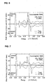
- FIG 6 shows the electron state density of V in ZnTe in a half-metallic (an upward spin means a metal state, and a downward spin means semiconductor) state.
- FIG. 7 shows the electron state density of Cr in ZnTe in a half-metallic (an upward spin means a metal state, and a downward spin means a semiconductor) state.
- the ferromagnetic interaction between spins and the ferromagnetic transition temperature can be controllably adjusted by changing the concentration of V or Cr. From a practical standpoint, the ferromagnetic transition temperature is preferably adjusted to be 300°K or more.
- V and Cr and different one or more anti-ferromagnetic transition metal elements can be mixed-crystallized to adjust the state of hole or electron, and have the respective magnetic characteristics.
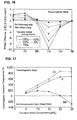
- the transition metal of V or Cr, and Mn having anti-ferromagnetism were mixed-crystallized.
- the total concentration of V and Mn, or Cr and Mn was set at 25 at%, and "x" in Cr 0.25-x Mn x Zn 0.75 Te was variously changed.
- the result is shown in FIG 4.
- V and Mn can be mixed-crystallized at the concentration of 25 at%, and "x" in V 0.25-x Mn x Zn 0.75 Te can be variously changed. While not illustrated, a magnetic moment can be obtained depending on the ratio of V to Mn.
- an n-type or p-type dopant may be doped, and the amount of hole or electron can also be changed to change the ferromagnetic state.
- the n-type or p-type dopant enters in the conductive band or valence band of ZnTe, and acts on d-electrons of the transition metal element close to the band.
- the doped dopant is not effective in its entirety, it acts on d-electrons to change the ferromagnetic state and the ferromagnetic transition temperature.
- the doping of the n-type dopant is equivalent to supply of an electron.
- the above effect from adding V or Cr, and Mn can also be achieved by doping the n-type dopant while crystallizing V or Cr.
- the doping of the p-type dopant together with Cr can obtain the same effect as that from the addition of V to Cr as described above.
- the transition metal element such as V does not have such a significant change to the anti-ferromagnetic spin glass state, because it originally exhibits ferromagnetism, it can change the ferromagnetic state and ferromagnetic transition temperature in the same level.
- the magnetic moment itself is maintained at a value determined by the kind of transition material crystallized in ZnTe.
- the n-type dopant may include B, Al, In, Ga, Zn or Cl, Br or H, and a chalcogen compound thereof may be used as the material of the dopant.
- a donor concentration is 1 ⁇ 10 18 cm -3 or more.
- the doping at about 10 20 to 10 21 cm -3 is equivalent to the aforementioned mixed ratio of about 1 to 10 %.
- the p-type dopant may include an atomic N or N + or excited N 2 , as described above. In this case, while the p-type dopant involves the difficulty in doping, a small amount of the n-type dopant can be simultaneously doped to increase the concentration of the p-type dopant.
- the transmittable minimum wavelength of a Group II-VI compound with the transition metal is varied depending on whether the transition metal is V or Cr, and at least one of V and Cr and one or more different transition materials can be mixed-crystallized to adjust the minimum wavelength of transmittable light while transmittance or refraction as light-transmittance characteristics is not so changed, so as to form a light filter for cutting light of less than a desired wavelength.
- the present invention provides a Group II-VI compound-based ferromagnetic material capable of transmitting light having a desired wavelength.
- V or Cr is crystallized in ZnTe at 25 at%, the minimum wavelength of transmittable light was measured as show in Table 3.
- Kind of Transition metal Concentration of Transition Metal (at %) Minimum Wavelength (nm) ZnTe: V 25 495 ZnTe: Cr 25 562
- a ferromagnetic magnet transparent to light having a desired wavelength can be obtained.
- a Group III-V non-nitride-based single-crystal ferromagnetic material of the present invention at least one transition metal selected from the group consisting of V and Cr is substituted for the Group III element of a Group III-V compound.
- the Group III-V non-nitride herein means an arsenic compound or phosphorus compound including Ga or In, and specifically GsAs, InAs, GaP and InP.
- the aforementioned transition metal element has an ion radius close to that of a Group III element such as Ga or In.
- the transition metal element even if about 25 at % or more of Ga or In in the Group III-V compound is substituted with the transition metal element, it can maintain a single crystal having a zinc blende structure, and exhibits a ferromagnetic property in a zinc blende structure while maintaining its transparency to light ranging from the red to far-infrared wavelength.
- the Group III-V non-nitride-based single-crystal ferromagnetic material may include the above transition metal element, and at least one metal element selected from the group consisting of Ti, Mn, Fe, Co, Ni, Cu, Rh and Ru.
- each of the metal elements has a different state of d-electron, and thus ferromagnetic characteristics are more directly changed as compared to the doping of hole or electron to allow ferromagnetic characteristics such as a ferromagnetic transition temperature to be adjusted.
- the inventors have made various researches for obtaining a ferromagnetic material using a Group III-V compound.
- the transition metal element V or Cr allows d-electrons to be released therefrom more than Fe exhibiting anti-ferromagnetism by three, and thus, as seen from FIG 9 showing the difference ⁇ E between the entire energy of an antiferromagnetic spin glass state and the entire energy of a ferromagnetic state in GaAs, the mixed crystal can exhibit ferromagnetism only by crystallizing V or Cr in the Group III-V compound independently.
- FIG 9 shows examples in which the mixed ratio of the crystallized transition metal element to Ga of GaAs is arranged at 5, 10, 15, 20 and 25 at %.
- the mixed crystal exhibits ferromagnetism even at the mixed ratio of several %, and the crystallization and transparency are not degraded even if the ratio is increased.
- the mixed ratio is can be set in the range of 1 to 100 at %, preferably 5 to 25 at % to provide sufficient ferromagnetism.
- the kind of the transition metal element is not limited to one, but two or more kinds of transition metal elements may be crystallized (alloyed) together as described later.
- a thin film of the GaAs compound containing the above transition metal element can be formed, for example, by using an MBE apparatus as schematically shown in FIG 9.
- a substrate 5, such as sapphire, for growing a GaAs compound is placed on a substrate holder 4 contained in a chamber 1 capable of maintaining a ultra-high-vacuum of about 1.33 ⁇ 10 -6 Pa, and a heater 7 is operable to heat the substrate 5.
- the MBE apparatus includes: a cell 2a disposed opposed to the substrate 5 held by the substrate holder 4, and containing Ga as a material (source) of an element constituting a compound to be grown; a cell 2b (while Fig. 1 shows only one cell, two or more cells will be provided if two or more transition metal elements are crystallized together) containing a transition metal element such as V or Cr; a cell 2c containing an n-type dopant of Sn; an RF radical cell 3a for generating a radical oxygen O as an n-type dopant; and a cell 2d containing a p-type dopant of Zn.
- the solid material such as Ga, In or transition metal may be contained in a cell in the form of its metal oxide, and heated into an atomic form.
- Each of the materials of Zn, In, transition metal element and n-type dopant is prepared by atomizing a solid source having a purity of 99.99999 %.
- O + or O 2 in an excited state is prepared by activating an O 2 molecule using the above radical cell.
- Sn or transition metal element can be atomized by irradiating thire molecular gas with an electromagnetic wave in a microwave range.
- the n-type dopant of Sn, the p-type dopant of atomic Zn, and, for example, an atomic transition element of V or Cr are simultaneously supplied on the substrate 5, respectively, at a flow rate of 1.33 ⁇ 10 -5 Pa, 6.65 ⁇ 10 -5 Pa, and 1.33 ⁇ 10 -5 Pa, while growing GaAs at 350 to 750°C to form a film. In this way, a GaAs thin film 6 with V or Cr crystallized therein can be obtained.
- FIG 9 and after-mentioned Tables 4 and 5 show an example of doping only V or Cr without doping any dopant.
- the difference ⁇ E between the entire energy of an antiferromagnetic spin glass state and the entire energy of a ferromagnetic state is 1.3 ⁇ 13.6 meV in V and 2.1 ⁇ 13.6 meV in Cr, to provide ferromagnetism.
- the data in FIG 9 is obtained through a first principle calculation (simulation using an atomic number as an input parameter), and the dependency on the concentration of each of the transition metal elements is shown therein.
- Fe, Co or Ni will be an anti-ferromagnetic spin glass.
- the transition metal element is doped in the GaAs compound in the above example, a GaAs-based compound in which a part of Ga in GaAs is substituted with another Group III element such as In or B is different in bandgap, but has a similar structure to that of GaAs.
- the GaAs-based compound can also provide a ferromagnetic single-crystal in the same way.
- the transition metal element having approximately the same ion radius as that of Ga is mixed-crystallized, and thus Ga 3+ is substituted with V 2+ or Cr 2+ to maintain the zinc blende structure.
- V or Cr has an electron structure allowing d-electrons to be reduced more than that of Mn, and a ferromagnetic state can be maintained as it is, as shown in FIG 9.
- the ferromagnetic GaAs had a large magnetic moment, and can provide Cr-contained GaAs-based compound material, for example a magnetic moment of 3.00 ⁇ 9.274 J/T (3.00 ⁇ B (Bohr magneton)) as shown in after-mentioned Tables 4 and 5.
- the GaAs-based compound material provides a ferromagnetic magnet having extremely strong magnetism.
- FIG 13 shows the electron state density of V in GaAs in a half-metallic (an upward spin means a metal state, and a downward spin means semiconductor) state.
- FIG 14 shows the electron state density of Cr in GaAs in a half-metallic (an upward spin means a metal state, and a downward spin means a semiconductor) state.
- the ferromagnetic interaction between spins and the ferromagnetic transition temperature can be controllably adjusted by changing the concentration of V or Cr. From a practical standpoint, the ferromagnetic transition temperature is preferably adjusted to be 300°K or more.
- V and Cr and different one or more anti-ferromagnetic transition metal elements can be mixed-crystallized to adjust the state of hole or electron, and have the respective magnetic characteristics.
- the transition metal of V or Cr, and Fe having anti-ferromagnetism were mixed-crystallized.
- the total concentration of V and Fe, or Cr and Fe was set at 25 at%, and "x" in Cr 0.25-x Fe x Ga 0.75 As was variously changed.
- the result is shown in FIG 11.
- an n-type or p-type dopant may be doped, and the amount of hole or electron can also be changed to change the ferromagnetic state.
- the n-type or p-type dopant enters in the conductive band or valence band of GaAs, and acts on d-electrons of the transition metal element close to the band.
- the doped dopant is not effective in its entirety, it acts on d-electrons to change the ferromagnetic state and the ferromagnetic transition temperature.
- the doping of the n-type dopant is equivalent to supply of an electron.
- the above effect from adding V or Cr, and Fe can also be achieved by doping the n-type dopant while crystallizing V or Cr.
- the doping of the p-type dopant together with Cr can obtain the same effect as that from the addition of V to Cr as described above.
- the transition metal element such as V does not have such a significant change to the anti-ferromagnetic spin glass state, because it originally exhibits ferromagnetism, it can change the ferromagnetic state and ferromagnetic transition temperature in the same level.
- the magnetic moment itself is maintained at a value determined by the kind of transition material crystallized in GaAs.
- the n-type dopant may include Sn, Se, S, Te or H, and an oxide thereof may be used as the material of the dopant.
- a donor concentration is 1 ⁇ 10 18 cm -3 or more.
- the doping at about 10 20 to 10 21 cm -3 is equivalent to the aforementioned mixed ratio of about 1 to 10 %.
- the p-type dopant may include an atomic Zn, as described above.
- a small amount of the n-type dopant can be simultaneously doped to increase the concentration of the p-type dopant.
- the transmittable minimum wavelength of a Group III-V non-nitride with the transition metal is varied depending on whether the transition metal is V or Cr, and at least one of V and Cr and one or more different transition materials can be mixed-crystallized to adjust the minimum wavelength of transmittable light while transmittance or refraction as light-transmittance characteristics is not so changed, so as to form a light filter for cutting light of less than a desired wavelength.
- the present invention provides a Group III-V compound-based ferromagnetic material capable of transmitting light having a desired wavelength.
- V or Cr is crystallized in GaAs at 25 at%, the minimum wavelength of transmittable light was measured as show in Table 6.
- Kind of Transition metal Concentration of Transition Metal (at %) Minimum Wavelength (nm) GaAs: V 25 700 GaAs: Cr 25 650
- a ferromagnetic magnet transparent to light having a desired wavelength can be obtained.
- a Group III-V nitride-based single-crystal ferromagnetic material of the present invention at least one transition metal selected from the group consisting of V, Cr and Mn is substituted for the Group III element of a Group III-V compound.
- the Group III-V nitride herein means a nitride including Ga, Al, In or B, and specifically GaN, AIN, InN and BN.
- the aforementioned transition metal element has an ion radius relatively close to that of a Group III element such as Ga, Al or In.
- the Group III-V nitride-based single-crystal ferromagnetic material may include the above transition metal element, and at least one metal element selected from the group consisting of Ti, Fe, Co, Ni, Cu, Rh and Ru.
- each of the metal elements has a different state of d-electron, and thus ferromagnetic characteristics are more directly changed as compared to the doping of hole or electron to allow ferromagnetic characteristics such as a ferromagnetic transition temperature to be adjusted.
- the inventors have made various researches for obtaining a ferromagnetic material using a Group III-V nitride.
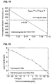
- the transition metal element V, Cr or Mn allows d-electrons to be released therefrom more than Fe exhibiting anti-ferromagnetism by three, and thus, as seen from FIG 16 showing the difference ⁇ E between the entire energy of an antiferromagnetic spin glass state and the entire energy of a ferromagnetic state in GaN, the mixed crystal can exhibit ferromagnetism only by crystallizing V, Cr or Mn in the Group III-V compound independently.
- FIG. 16 shows examples in which the mixed ratio of the crystallized transition metal element to Ga of GaN is arranged at 5, 10, 15, 20 and 25 at %.
- the mixed crystal exhibits ferromagnetism even at the mixed ratio of several %, and the crystallization and transparency are not degraded even if the ratio is increased.
- the mixed ratio is can be set in the range of 1 to 100 at %, preferably 5 to 25 at % to provide sufficient ferromagnetism.
- the kind of the transition metal element is not limited to one, but two or more kinds of transition metal elements may be crystallized (alloyed) together as described later.
- a thin film of the GaN compound containing the above transition metal element can be formed, for example, by using an MBE apparatus as schematically shown in FIG 15.
- a substrate 5, such as SIC or sapphire, for growing a GaN compound is placed on a substrate holder 4 contained in a chamber 1 capable of maintaining a ultra-high-vacuum of about 1.33 ⁇ 10 -6 Pa, and a heater 7 is operable to heat the substrate 5.
- the MBE apparatus includes: a cell 2a disposed opposed to the substrate 5 held by the substrate holder 4, and containing Ga as a material (source) of an element constituting a compound to be grown; a cell 2b (while Fig. 1 shows only one cell, two or more cells will be provided if two or more transition metal elements are crystallized together) containing a transition metal element such as V, Cr or Mn; a cell 2c containing an n-type dopant of Si, Ge or O; a cell 2d containing a p-type dopant of Mg, Be or C; an RF radical cell 3a for generating a radical nitrogen N.
- the solid material such as Ga or transition metal may be contained in a cell in the form of its metal oxide, and heated into an atomic form.
- Each of the materials of Ga, transition metal element and n-type dopant is prepared by atomizing a solid source having a purity of 99.99999 %.
- N + or N 2 in an excited state is prepared by activating an N 2 molecule or NH 3 using the above radical cell.
- Ga or transition metal element can be atomized by irradiating thire molecular gas with an electromagnetic wave in a microwave range.
- the n-type dopant of Si or O, the p-type dopant of atomic Mg, Be or C, and, for example, an atomic transition element of V, Cr or Mn are simultaneously supplied on the substrate 5, respectively, at a flow rate of 1.33 ⁇ 10 -5 Pa, 6.65 ⁇ 10 -5 Pa, and 1.33 ⁇ 10 -5 Pa, while growing GaN at 350 to 800°C to form a film. In this way, a GaAs thin film 6 with V or Cr crystallized therein can be obtained.
- FIG 16 and after-mentioned Tables 7 and 8 show an example of doping only V, Cr or Mn without doping any dopant.
- the difference ⁇ E between the entire energy of an antiferromagnetic spin glass state and the entire energy of a ferromagnetic state is 2.04 ⁇ 13.6 meV in V, 2.57 ⁇ 13.6 meV in Cr and 0.55 ⁇ 13.6 meV in Mn, to provide ferromagnetism.
- the data in FIG 16 is obtained through a first principle calculation (simulation using an atomic number as an input parameter), and the dependency on the concentration of each of the transition metal elements is shown therein.
- Fe, Co or Ni will be an anti-ferromagnetic spin glass.
- the transition metal element is doped in the GaN compound in the above example.
- a GaN-based compound in which a part of Ga in GaN is substituted with another Group III element such as Al or B the magnitude of its bandgap can be controlled, and the structure is the same as that of GaN except for the bandgap.
- the GaN-based compound can also provide a ferromagnetic single-crystal in the same way.
- the transition metal element having approximately the same ion radius as that of Ga is mixed-crystallized, and thus Ga 3+ is substituted with V 2+ , Cr 2+ or Mn 2+ to maintain the wurtzite structure.
- V, Cr or Mn has an electron structure allowing holes to be increased, and a ferromagnetic state can be maintained as it is, as shown in FIG. 16.
- the ferromagnetic GaN had a large magnetic moment, and can provide Cr-contained GaN-based compound material, for example a magnetic moment of 2.94 ⁇ 9.274 J/T (2.94 ⁇ B (Bohr magneton)) as shown in after-mentioned Tables 7 and 8.
- the GaN-based compound material provides a ferromagnetic magnet having extremely strong magnetism.
- FIG. 20 shows the electron state density of V in GaN in a half-metallic (an upward spin means a metal state, and a downward spin means semiconductor) state.
- FIG. 21 shows the electron state density of Cr in GaN in a half-metallic (an upward spin means a metal state, and a downward spin means a semiconductor) state.
- the ferromagnetic interaction between spins and the ferromagnetic transition temperature can be controllably adjusted by changing the concentration of V, Cr or Mn. From a practical standpoint, the ferromagnetic transition temperature is preferably adjusted to be 300°K or more.
- the inventors found that at least one of V, Cr and Mn and different one or more anti-ferromagnetic transition metal elements can be mixed-crystallized to adjust the state of hole or electron, and have the respective magnetic characteristics.
- the transition metal of V, Cr or Mn, and Fe having anti-ferromagnetism were mixed-crystallized.
- the total concentration of V and Fe, or Cr and Fe, or Mn and Fe was set at 25 at%, and "x" in V 0.25-x Fe x Ga 0.75 N was variously changed.
- the result is shown in FIGS 18.
- Cr or Mn and Fe can be mixed-crystallized at the total concentration of 25 at%, and "x" in Cr 0.25-x Fe x Ga 0.75 N, or Mn 0.25-x Fe x Ga 0.75 N can be variously changed. While not illustrated, a magnetic moment can be obtained depending on the ratio of V to Mn.
- an n-type or p-type dopant may be doped, and the amount of hole or electron can also be changed to change the ferromagnetic state.
- the n-type or p-type dopant enters in the conductive band or valence band of GaN, and acts on d-electrons of the transition metal element close to the band.
- the doped dopant is not effective in its entirety, it acts on d-electrons to change the ferromagnetic state and the ferromagnetic transition temperature.
- the doping of the n-type dopant is equivalent to supply of an electron.
- the above effect from adding V, Cr or Mn, and Fe can also be achieved by doping the n-type dopant while crystallizing V, Cr or Mn.
- the doping of the p-type dopant together with Mn can obtain the same effect as that from the addition of Cr to Mn as described above.
- the transition metal element such as V or Mn does not have such a significant change to the anti-ferromagnetic spin glass state, because it originally exhibits ferromagnetism, it can change the ferromagnetic state and ferromagnetic transition temperature in the same level.
- the magnetic moment itself is maintained at a value determined by the kind of transition material crystallized in GaN.
- the n-type dopant may include Sn, Ge or O, and a nitride thereof may be used as the material of the dopant.
- a donor concentration is 1 ⁇ 10 18 cm -3 or more.
- the doping at about 10 20 to 10 21 cm -3 is equivalent to the aforementioned mixed ratio of about 1 to 10%.
- the p-type dopant may include a Mg, Be or C, as described above.
- a small amount of the n-type dopant can be simultaneously doped to increase the concentration of the p-type dopant.
- the transmittable minimum wavelength of a Group III-V nitride with the transition metal is varied depending on whether the transition metal is V, Cr or Mn, and at least one of V, Cr and Mn and one or more different transition materials can be mixed-crystallized to adjust the minimum wavelength of transmittable light while transmittance or refraction as light-transmittance characteristics is not so changed, so as to form a light filter for cutting light of less than a desired wavelength.
- the present invention provides a Group III-V nitride-based ferromagnetic material capable of transmitting light having a desired wavelength.
- V, Cr or Mn is crystallized in GaN at 25 at%, the minimum wavelength of transmittable light was measured as show in Table 9.
- Kind of Transition metal Concentration of Transition Metal (at %) Minimum Wavelength (nm) GaN: V 25 400 GaN: Cr 25 390 GaN: Mn 25 380
- a ferromagnetic magnet transparent to light having a desired wavelength can be obtained.
- the kinetic energy of hole or electron introduced a metal element itself to be mixed-crystallized can change the entire energy, and hole or electron to be introduced can be adjusted by reducing the entire energy to provide a stabilized ferromagnetic state
- the magnitude and sign of the magnetic interaction between metal atoms are changed depending on hole or electron to be introduced.
- the ferromagnetic state can be stabilized by controlling the hole or electron
- an MBE (molecular beam epitaxy) apparatus has been used for forming the Group II-VI or III-V compound thin film in the above example
- an MOCVD (metalorganic chemical vapor deposition) apparatus may be used to form the film.
- the metal material of Zn, Cd, Ga, In, Al or transition metal is introduced in the MOCVD apparatus, in the form of an organic metal compound such as dimethyl zinc, dimethyl gallium or dimethyl aluminum.
- the thin film is formed in a nonequilibrium state to allow the transition metal material to be doped at a desired concentration.
- the film forming method is not limited to these methods, but a laser abrasion method may be used in which a film is formed while blowing an activated dopant onto a substrate, using a target, such as a target Zn sulfate (selenide) solid, transition-metal-elemental material or sulfate (selenide) solid, or Ga, In solid, transition-metal-elemental material or compound solid, Ga nitrided solid or Al nitride solid.
- a target such as a target Zn sulfate (selenide) solid, transition-metal-elemental material or sulfate (selenide) solid, or Ga, In solid, transition-metal-elemental material or compound solid, Ga nitrided solid or Al nitride solid.
- an ECR plasma for antagonizing an object by electronically exciting with radio waved, leaser, X-ray or electron beam may be used.
- the ECR plasma may be used in an n-type dopant or a p-type dopant.
- the ECR makes it possible to form a dopant in an atomic state and dope it in high concentration.
- a ferromagnetic single crystal can be obtained only by mixing at least one of V and Cr into Group II-VI compound or Group III-V non-nitride, or by mixing at least one of V, Cr or Mn and Mn into Group III-V nitride.
- the ferromagnetic single crystal can be combined with a ZnO or transparent conductive oxide (TCO), which is used as an n-type and p-type transparent electrode, or optical fibers, to open the way to realize a quantum computer or a high-capacity magnetooptical recording, and can provide an optical electronics material usable in from visible to ultraviolet range which is applicable to high-performance information communication or a quantum computer.
- TCO transparent conductive oxide
Landscapes
- Chemical & Material Sciences (AREA)
- Engineering & Computer Science (AREA)
- Crystallography & Structural Chemistry (AREA)
- Materials Engineering (AREA)
- Metallurgy (AREA)
- Organic Chemistry (AREA)
- Inorganic Chemistry (AREA)
- Hard Magnetic Materials (AREA)
- Crystals, And After-Treatments Of Crystals (AREA)
Applications Claiming Priority (7)
| Application Number | Priority Date | Filing Date | Title |
|---|---|---|---|
| JP2001059164 | 2001-03-02 | ||
| JP2001059195 | 2001-03-02 | ||
| JP2001059195A JP3989182B2 (ja) | 2001-03-02 | 2001-03-02 | 強磁性iii−v族系化合物及びその強磁性特性の調整方法 |
| JP2001059303A JP3938284B2 (ja) | 2001-03-02 | 2001-03-02 | 強磁性GaN系混晶化合物及びその強磁性特性の調整方法 |
| JP2001059164A JP3998425B2 (ja) | 2001-03-02 | 2001-03-02 | 強磁性ii−vi族系化合物及びその強磁性特性の調整方法 |
| JP2001059303 | 2001-03-02 | ||
| PCT/JP2002/001889 WO2002070793A1 (fr) | 2001-03-02 | 2002-02-28 | Compose ferromagnetique monocristallin sur la base du groupe ii-vi ou du groupe iii-v et procede pour adapter ses caracteristiques ferromagnetiques |
Publications (1)
| Publication Number | Publication Date |
|---|---|
| EP1367151A1 true EP1367151A1 (de) | 2003-12-03 |
Family
ID=27346161
Family Applications (1)
| Application Number | Title | Priority Date | Filing Date |
|---|---|---|---|
| EP02701657A Withdrawn EP1367151A1 (de) | 2001-03-02 | 2002-02-28 | Einkristalline ferromagnetische verbindung auf gruppe-ii-vi- oder gruppe-iii-v-basis und verfahren zur einstellung ihrer ferromagnetischen eigenschaften |
Country Status (6)
| Country | Link |
|---|---|
| US (1) | US20040112278A1 (de) |
| EP (1) | EP1367151A1 (de) |
| KR (1) | KR100531514B1 (de) |
| CN (1) | CN1313656C (de) |
| TW (1) | TWI254088B (de) |
| WO (1) | WO2002070793A1 (de) |
Cited By (2)
| Publication number | Priority date | Publication date | Assignee | Title |
|---|---|---|---|---|
| EP1388597A4 (de) * | 2001-04-04 | 2008-05-21 | Nippon Mining Co | VERFAHREN ZUR HERSTELLUNG VON ZnTe-VERBINDUNGSHALBLEITER-EINKRISTALL, ZNTE-VERBINDUNGSHALBLEITER-EINKRISTALL UND HALBLEITERVORRICHTUNG |
| RU2456073C1 (ru) * | 2011-04-20 | 2012-07-20 | Государственное Образовательное Учреждение Высшего Профессионального Образования "Омский Государственный Технический Университет" | Катализатор окисления оксида углерода |
Families Citing this family (11)
| Publication number | Priority date | Publication date | Assignee | Title |
|---|---|---|---|---|
| US7606274B2 (en) * | 2001-09-20 | 2009-10-20 | The Uab Research Foundation | Mid-IR instrument for analyzing a gaseous sample and method for using the same |
| US8817830B2 (en) * | 2002-09-19 | 2014-08-26 | The Uab Research Foundation | Saturable absorbers for Q-switching of middle infrared laser cavaties |
| US6960486B2 (en) * | 2001-09-20 | 2005-11-01 | University Of Alabama At Brimingham Research Foundation | Mid-IR microchip laser: ZnS:Cr2+ laser with saturable absorber material |
| JP3979138B2 (ja) | 2001-12-20 | 2007-09-19 | 住友電気工業株式会社 | 光アイソレータおよび偏光子 |
| KR100499180B1 (ko) * | 2002-12-14 | 2005-07-01 | 강태원 | 양자점 구조를 갖는 강자성 반도체 제조방법 |
| SE0300352D0 (sv) * | 2003-02-06 | 2003-02-06 | Winto Konsult Ab | Ferromagnetism in semiconductors |
| JP4034208B2 (ja) * | 2003-02-25 | 2008-01-16 | ローム株式会社 | 透明電極 |
| JP4708334B2 (ja) * | 2004-02-27 | 2011-06-22 | 独立行政法人科学技術振興機構 | 透明強磁性単結晶化合物の製造方法 |
| JPWO2006028299A1 (ja) * | 2004-09-10 | 2008-05-08 | 国立大学法人大阪大学 | 反強磁性ハーフメタリック半導体及びその製造方法 |
| CN102776568B (zh) * | 2011-05-13 | 2015-09-16 | 中国科学院物理研究所 | 一种激光晶体及其制备方法和用途 |
| JP6398744B2 (ja) * | 2015-01-23 | 2018-10-03 | 三菱電機株式会社 | 半導体デバイス用基板の製造方法 |
Family Cites Families (7)
| Publication number | Priority date | Publication date | Assignee | Title |
|---|---|---|---|---|
| JPS5419079B2 (de) * | 1974-08-15 | 1979-07-12 | ||
| JPS5544721A (en) * | 1978-09-27 | 1980-03-29 | Natl Res Inst For Metals | Extraneous semiconductor joining matter and its preparation |
| CN85101849B (zh) * | 1985-04-01 | 1986-12-03 | 中国科学院长春物理研究所 | 制备高纯度ⅱb-ⅵa族化合物的新方法 |
| DE69008770T2 (de) * | 1989-05-31 | 1994-11-24 | Ibm | Magnetische Materialien für Festkörpervorrichtungen. |
| JP3719613B2 (ja) * | 1995-04-24 | 2005-11-24 | シャープ株式会社 | 半導体発光素子 |
| JP4421065B2 (ja) * | 2000-04-07 | 2010-02-24 | 株式会社アルバック | トンネル磁気抵抗素子の製造方法、トンネル磁気抵抗素子 |
| AU2003222000A1 (en) * | 2002-03-14 | 2003-09-29 | Wisys Technology Foundation, Inc. | Mbe-method for the production of a gallium manganese nitride ferromagnetic film |
-
2002
- 2002-02-28 EP EP02701657A patent/EP1367151A1/de not_active Withdrawn
- 2002-02-28 KR KR10-2003-7011104A patent/KR100531514B1/ko not_active Expired - Fee Related
- 2002-02-28 CN CNB028058283A patent/CN1313656C/zh not_active Expired - Fee Related
- 2002-02-28 US US10/468,833 patent/US20040112278A1/en not_active Abandoned
- 2002-02-28 WO PCT/JP2002/001889 patent/WO2002070793A1/ja not_active Ceased
- 2002-03-01 TW TW091103879A patent/TWI254088B/zh not_active IP Right Cessation
Non-Patent Citations (1)
| Title |
|---|
| See references of WO02070793A1 * |
Cited By (6)
| Publication number | Priority date | Publication date | Assignee | Title |
|---|---|---|---|---|
| EP1388597A4 (de) * | 2001-04-04 | 2008-05-21 | Nippon Mining Co | VERFAHREN ZUR HERSTELLUNG VON ZnTe-VERBINDUNGSHALBLEITER-EINKRISTALL, ZNTE-VERBINDUNGSHALBLEITER-EINKRISTALL UND HALBLEITERVORRICHTUNG |
| US7517720B2 (en) | 2001-04-04 | 2009-04-14 | Nippon Mining & Metals Co., Ltd. | Method for producing ZnTe system compound semiconductor single crystal, ZnTe system compound semiconductor single crystal, and semiconductor device |
| US7521282B2 (en) | 2001-04-04 | 2009-04-21 | Nippon Mining & Metals Co., Ltd. | Method for producing ZnTe system compound semiconductor single crystal, ZnTe system compound semiconductor single crystal, and semiconductor device |
| US7629625B2 (en) | 2001-04-04 | 2009-12-08 | Nippon Mining & Metals Co., Ltd. | Method for producing ZnTe system compound semiconductor single crystal, ZnTe system compound semiconductor single crystal, and semiconductor device |
| US7696073B2 (en) | 2001-04-04 | 2010-04-13 | Nippon Mining & Metals Co., Ltd. | Method of co-doping group 14 (4B) elements to produce ZnTe system compound semiconductor single crystal |
| RU2456073C1 (ru) * | 2011-04-20 | 2012-07-20 | Государственное Образовательное Учреждение Высшего Профессионального Образования "Омский Государственный Технический Университет" | Катализатор окисления оксида углерода |
Also Published As
| Publication number | Publication date |
|---|---|
| KR100531514B1 (ko) | 2005-11-28 |
| CN1494607A (zh) | 2004-05-05 |
| TWI254088B (en) | 2006-05-01 |
| CN1313656C (zh) | 2007-05-02 |
| US20040112278A1 (en) | 2004-06-17 |
| KR20030088436A (ko) | 2003-11-19 |
| WO2002070793A1 (fr) | 2002-09-12 |
Similar Documents
| Publication | Publication Date | Title |
|---|---|---|
| Tanaka et al. | Molecular beam epitaxy of MnAs thin films on GaAs | |
| US20060108619A1 (en) | Ferromagnetic IV group based semiconductor, ferromagnetic III-V group based compound semiconductor, or ferromagnetic II-IV group based compound semiconductor, and method for adjusting their ferromagnetic characteristics | |
| US6527858B1 (en) | P-type ZnO single crystal and method for producing the same | |
| EP1367151A1 (de) | Einkristalline ferromagnetische verbindung auf gruppe-ii-vi- oder gruppe-iii-v-basis und verfahren zur einstellung ihrer ferromagnetischen eigenschaften | |
| US5187116A (en) | Process for preparing electroluminescent device of compound semiconductor | |
| EP1215310A1 (de) | P-typ zinkoxid-einkristall mit niedrigem widerstand und herstellungsverfahren dafür | |
| US7115213B2 (en) | Ferromagnetic ZnO-type compound including transition metallic element and method for adjusting ferromagnetic characteristics thereof | |
| US7022182B1 (en) | Ferromagnetic p-type single-crystal zinc oxide material and manufacturing method thereof | |
| US5100832A (en) | Process for preparing epitaxial compound semiconductor | |
| Setzler et al. | Observation of singly ionized selenium vacancies in ZnSe grown by molecular beam epitaxy | |
| JP3998425B2 (ja) | 強磁性ii−vi族系化合物及びその強磁性特性の調整方法 | |
| US20060231789A1 (en) | Transparent ferromagnetic alkali/chalcogenide compound comprising solid solution of transition metal or rare earth metal and method of regulating ferromagnetism thereof | |
| JP3989182B2 (ja) | 強磁性iii−v族系化合物及びその強磁性特性の調整方法 | |
| JP3938284B2 (ja) | 強磁性GaN系混晶化合物及びその強磁性特性の調整方法 | |
| US20070178032A1 (en) | Transparent ferromagnetic compound containing no magnetic impurity such as transition metal or rare earth metal and forming solid solution with element having imperfect shell, and method for adjusting ferromagnetic characteristics thereof | |
| Catalan | 7568. Formation of patterned tin oxide thin films by ion beam decomposition of metallo-organies | |
| Jin et al. | Pulsed Laser Deposition and Characterization of Zn1− xMnxO Films | |
| Yoshimoto et al. | GaNAsBi semiconductor alloy with temperature-insensitive bandgap | |
| JPH08236551A (ja) | 化合物半導体の製造方法および半導体発光素子 |
Legal Events
| Date | Code | Title | Description |
|---|---|---|---|
| PUAI | Public reference made under article 153(3) epc to a published international application that has entered the european phase |
Free format text: ORIGINAL CODE: 0009012 |
|
| 17P | Request for examination filed |
Effective date: 20030902 |
|
| AK | Designated contracting states |
Kind code of ref document: A1 Designated state(s): AT BE CH CY DE DK ES FI FR GB GR IE IT LI LU MC NL PT SE TR |
|
| RAP1 | Party data changed (applicant data changed or rights of an application transferred) |
Owner name: JAPAN SCIENCE AND TECHNOLOGY AGENCY |
|
| STAA | Information on the status of an ep patent application or granted ep patent |
Free format text: STATUS: THE APPLICATION HAS BEEN WITHDRAWN |
|
| 18W | Application withdrawn |
Effective date: 20070823 |