EP1369917A2 - Plaque de montage pour composants électroniques, méthode de fabrication associée, module de composants électroniques et appareil de communication - Google Patents
Plaque de montage pour composants électroniques, méthode de fabrication associée, module de composants électroniques et appareil de communication Download PDFInfo
- Publication number
- EP1369917A2 EP1369917A2 EP03012908A EP03012908A EP1369917A2 EP 1369917 A2 EP1369917 A2 EP 1369917A2 EP 03012908 A EP03012908 A EP 03012908A EP 03012908 A EP03012908 A EP 03012908A EP 1369917 A2 EP1369917 A2 EP 1369917A2
- Authority
- EP
- European Patent Office
- Prior art keywords
- board
- electronic component
- via hole
- metallic body
- cushioning material
- Prior art date
- Legal status (The legal status is an assumption and is not a legal conclusion. Google has not performed a legal analysis and makes no representation as to the accuracy of the status listed.)
- Granted
Links
Images



Classifications
-
- H—ELECTRICITY
- H05—ELECTRIC TECHNIQUES NOT OTHERWISE PROVIDED FOR
- H05K—PRINTED CIRCUITS; CASINGS OR CONSTRUCTIONAL DETAILS OF ELECTRIC APPARATUS; MANUFACTURE OF ASSEMBLAGES OF ELECTRICAL COMPONENTS
- H05K1/00—Printed circuits
- H05K1/02—Details
- H05K1/0213—Electrical arrangements not otherwise provided for
- H05K1/0237—High frequency adaptations
- H05K1/0243—Printed circuits associated with mounted high frequency components
-
- H—ELECTRICITY
- H05—ELECTRIC TECHNIQUES NOT OTHERWISE PROVIDED FOR
- H05K—PRINTED CIRCUITS; CASINGS OR CONSTRUCTIONAL DETAILS OF ELECTRIC APPARATUS; MANUFACTURE OF ASSEMBLAGES OF ELECTRICAL COMPONENTS
- H05K1/00—Printed circuits
- H05K1/02—Details
- H05K1/0201—Thermal arrangements, e.g. for cooling, heating or preventing overheating
- H05K1/0203—Cooling of mounted components
- H05K1/0204—Cooling of mounted components using means for thermal conduction connection in the thickness direction of the substrate
-
- H—ELECTRICITY
- H10—SEMICONDUCTOR DEVICES; ELECTRIC SOLID-STATE DEVICES NOT OTHERWISE PROVIDED FOR
- H10W—GENERIC PACKAGES, INTERCONNECTIONS, CONNECTORS OR OTHER CONSTRUCTIONAL DETAILS OF DEVICES COVERED BY CLASS H10
- H10W40/00—Arrangements for thermal protection or thermal control
- H10W40/20—Arrangements for cooling
- H10W40/22—Arrangements for cooling characterised by their shape, e.g. having conical or cylindrical projections
- H10W40/226—Arrangements for cooling characterised by their shape, e.g. having conical or cylindrical projections characterised by projecting parts, e.g. fins to increase surface area
- H10W40/228—Arrangements for cooling characterised by their shape, e.g. having conical or cylindrical projections characterised by projecting parts, e.g. fins to increase surface area the projecting parts being wire-shaped or pin-shaped
-
- H—ELECTRICITY
- H10—SEMICONDUCTOR DEVICES; ELECTRIC SOLID-STATE DEVICES NOT OTHERWISE PROVIDED FOR
- H10W—GENERIC PACKAGES, INTERCONNECTIONS, CONNECTORS OR OTHER CONSTRUCTIONAL DETAILS OF DEVICES COVERED BY CLASS H10
- H10W44/00—Electrical arrangements for controlling or matching impedance
- H10W44/20—Electrical arrangements for controlling or matching impedance at high-frequency [HF] or radio frequency [RF]
-
- H—ELECTRICITY
- H05—ELECTRIC TECHNIQUES NOT OTHERWISE PROVIDED FOR
- H05K—PRINTED CIRCUITS; CASINGS OR CONSTRUCTIONAL DETAILS OF ELECTRIC APPARATUS; MANUFACTURE OF ASSEMBLAGES OF ELECTRICAL COMPONENTS
- H05K1/00—Printed circuits
- H05K1/02—Details
- H05K1/03—Use of materials for the substrate
- H05K1/0306—Inorganic insulating substrates, e.g. ceramic, glass
-
- H—ELECTRICITY
- H05—ELECTRIC TECHNIQUES NOT OTHERWISE PROVIDED FOR
- H05K—PRINTED CIRCUITS; CASINGS OR CONSTRUCTIONAL DETAILS OF ELECTRIC APPARATUS; MANUFACTURE OF ASSEMBLAGES OF ELECTRICAL COMPONENTS
- H05K2201/00—Indexing scheme relating to printed circuits covered by H05K1/00
- H05K2201/08—Magnetic details
- H05K2201/083—Magnetic materials
- H05K2201/086—Magnetic materials for inductive purposes, e.g. printed inductor with ferrite core
-
- H—ELECTRICITY
- H05—ELECTRIC TECHNIQUES NOT OTHERWISE PROVIDED FOR
- H05K—PRINTED CIRCUITS; CASINGS OR CONSTRUCTIONAL DETAILS OF ELECTRIC APPARATUS; MANUFACTURE OF ASSEMBLAGES OF ELECTRICAL COMPONENTS
- H05K2201/00—Indexing scheme relating to printed circuits covered by H05K1/00
- H05K2201/09—Shape and layout
- H05K2201/09009—Substrate related
- H05K2201/09063—Holes or slots in insulating substrate not used for electrical connections
-
- H—ELECTRICITY
- H05—ELECTRIC TECHNIQUES NOT OTHERWISE PROVIDED FOR
- H05K—PRINTED CIRCUITS; CASINGS OR CONSTRUCTIONAL DETAILS OF ELECTRIC APPARATUS; MANUFACTURE OF ASSEMBLAGES OF ELECTRICAL COMPONENTS
- H05K2201/00—Indexing scheme relating to printed circuits covered by H05K1/00
- H05K2201/10—Details of components or other objects attached to or integrated in a printed circuit board
- H05K2201/10227—Other objects, e.g. metallic pieces
- H05K2201/10416—Metallic blocks or heatsinks completely inserted in a PCB
-
- H—ELECTRICITY
- H05—ELECTRIC TECHNIQUES NOT OTHERWISE PROVIDED FOR
- H05K—PRINTED CIRCUITS; CASINGS OR CONSTRUCTIONAL DETAILS OF ELECTRIC APPARATUS; MANUFACTURE OF ASSEMBLAGES OF ELECTRICAL COMPONENTS
- H05K3/00—Apparatus or processes for manufacturing printed circuits
- H05K3/40—Forming printed elements for providing electric connections to or between printed circuits
- H05K3/4038—Through-connections; Vertical interconnect access [VIA] connections
- H05K3/4046—Through-connections; Vertical interconnect access [VIA] connections using auxiliary conductive elements, e.g. metallic spheres, eyelets, pieces of wire
-
- H—ELECTRICITY
- H10—SEMICONDUCTOR DEVICES; ELECTRIC SOLID-STATE DEVICES NOT OTHERWISE PROVIDED FOR
- H10W—GENERIC PACKAGES, INTERCONNECTIONS, CONNECTORS OR OTHER CONSTRUCTIONAL DETAILS OF DEVICES COVERED BY CLASS H10
- H10W72/00—Interconnections or connectors in packages
- H10W72/071—Connecting or disconnecting
- H10W72/072—Connecting or disconnecting of bump connectors
- H10W72/07251—Connecting or disconnecting of bump connectors characterised by changes in properties of the bump connectors during connecting
-
- H—ELECTRICITY
- H10—SEMICONDUCTOR DEVICES; ELECTRIC SOLID-STATE DEVICES NOT OTHERWISE PROVIDED FOR
- H10W—GENERIC PACKAGES, INTERCONNECTIONS, CONNECTORS OR OTHER CONSTRUCTIONAL DETAILS OF DEVICES COVERED BY CLASS H10
- H10W72/00—Interconnections or connectors in packages
- H10W72/071—Connecting or disconnecting
- H10W72/075—Connecting or disconnecting of bond wires
-
- H—ELECTRICITY
- H10—SEMICONDUCTOR DEVICES; ELECTRIC SOLID-STATE DEVICES NOT OTHERWISE PROVIDED FOR
- H10W—GENERIC PACKAGES, INTERCONNECTIONS, CONNECTORS OR OTHER CONSTRUCTIONAL DETAILS OF DEVICES COVERED BY CLASS H10
- H10W72/00—Interconnections or connectors in packages
- H10W72/20—Bump connectors, e.g. solder bumps or copper pillars; Dummy bumps; Thermal bumps
-
- H—ELECTRICITY
- H10—SEMICONDUCTOR DEVICES; ELECTRIC SOLID-STATE DEVICES NOT OTHERWISE PROVIDED FOR
- H10W—GENERIC PACKAGES, INTERCONNECTIONS, CONNECTORS OR OTHER CONSTRUCTIONAL DETAILS OF DEVICES COVERED BY CLASS H10
- H10W72/00—Interconnections or connectors in packages
- H10W72/50—Bond wires
- H10W72/551—Materials of bond wires
-
- H—ELECTRICITY
- H10—SEMICONDUCTOR DEVICES; ELECTRIC SOLID-STATE DEVICES NOT OTHERWISE PROVIDED FOR
- H10W—GENERIC PACKAGES, INTERCONNECTIONS, CONNECTORS OR OTHER CONSTRUCTIONAL DETAILS OF DEVICES COVERED BY CLASS H10
- H10W72/00—Interconnections or connectors in packages
- H10W72/90—Bond pads, in general
- H10W72/951—Materials of bond pads
-
- H—ELECTRICITY
- H10—SEMICONDUCTOR DEVICES; ELECTRIC SOLID-STATE DEVICES NOT OTHERWISE PROVIDED FOR
- H10W—GENERIC PACKAGES, INTERCONNECTIONS, CONNECTORS OR OTHER CONSTRUCTIONAL DETAILS OF DEVICES COVERED BY CLASS H10
- H10W72/00—Interconnections or connectors in packages
- H10W72/90—Bond pads, in general
- H10W72/951—Materials of bond pads
- H10W72/952—Materials of bond pads comprising metals or metalloids, e.g. PbSn, Ag or Cu
-
- H—ELECTRICITY
- H10—SEMICONDUCTOR DEVICES; ELECTRIC SOLID-STATE DEVICES NOT OTHERWISE PROVIDED FOR
- H10W—GENERIC PACKAGES, INTERCONNECTIONS, CONNECTORS OR OTHER CONSTRUCTIONAL DETAILS OF DEVICES COVERED BY CLASS H10
- H10W90/00—Package configurations
- H10W90/701—Package configurations characterised by the relative positions of pads or connectors relative to package parts
- H10W90/721—Package configurations characterised by the relative positions of pads or connectors relative to package parts of bump connectors
- H10W90/724—Package configurations characterised by the relative positions of pads or connectors relative to package parts of bump connectors between a chip and a stacked insulating package substrate, interposer or RDL
-
- H—ELECTRICITY
- H10—SEMICONDUCTOR DEVICES; ELECTRIC SOLID-STATE DEVICES NOT OTHERWISE PROVIDED FOR
- H10W—GENERIC PACKAGES, INTERCONNECTIONS, CONNECTORS OR OTHER CONSTRUCTIONAL DETAILS OF DEVICES COVERED BY CLASS H10
- H10W90/00—Package configurations
- H10W90/701—Package configurations characterised by the relative positions of pads or connectors relative to package parts
- H10W90/751—Package configurations characterised by the relative positions of pads or connectors relative to package parts of bond wires
- H10W90/754—Package configurations characterised by the relative positions of pads or connectors relative to package parts of bond wires between a chip and a stacked insulating package substrate, interposer or RDL
Definitions
- the present invention mainly relates to an electronic component mounting board used for a high-frequency part of a radio communication apparatus, for example, a transmission module for a radio communication apparatus, and an electronic component module using the board.
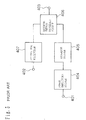
- FIG. 5 is a block diagram showing a state of using an antenna switch duplexer module and a power amplifier module in a conventional radio communication apparatus.
- reference numeral 406 denotes an antenna switch duplexer module
- reference numeral 404 denotes a power amplifier module
- reference numeral 405 denotes an isolator module
- reference numeral 407 denotes a filter for reception.
- the following will discuss the operations of the antenna switch duplexer module, the power amplifier module, and the radio communication apparatus that are configured thus.
- the antenna switch duplexer module is constituted by using a PIN diode and a compound semiconductor IC of GaAs and so on.
- the power amplifier module is constituted by using a compound semiconductor IC of GaAs, InGaP, and so on. Individually corresponding components are used for the filter for reception and the isolator module. These modules and the separate components are arranged on a printed board and are electrically connected via wiring such as a microstrip line.
- the miniaturization of the radio communication apparatus is limited and it is difficult to reduce the cost in the separate configurations.
- the connection is made by wiring on the printed board, impedance is disturbed at a high frequency, desired characteristics cannot be reproduced, and an adjustment step is necessary.
- the wiring on the printed board causes excessive loss and requires higher power consumption.
- a radio communication module is proposed in which separate modules such as an antenna switch 601, a power amplifier 602, and a VCO 603, and semiconductor components are flip-chip mounted on a thick-filmmultilayer board 600 including passive elements 604 (e.g., Japanese Patent Laid-Open No. 2002-261643).
- passive elements 604 e.g., Japanese Patent Laid-Open No. 2002-261643
- the entire disclosure of Japanese Patent Laid-Open No. 2002-261643 is incorporated herein by reference in its entirety.
- via holes 605 making electrical connection are used to release heat from components mounted on a board.
- the formation of vias arises a problem described below.
- the vias 605 are formed concurrently with the board by filling a metal such as aluminum having conductivity or a thermal conductivity into via holes, which are provided so as to penetrate a green sheet serving as a base of the board, and baking the green sheet thereafter.
- a metal such as aluminum having conductivity or a thermal conductivity
- the present invention has as its object the provision of an electronic component mounting board, which has an excellent heat releasing property and a low yield during manufacturing, and a method of manufacturing the same, and electronic component modules and so on whereby a smaller size and lower cost are readily achieved, desired characteristics can be realized with preferable reproducibility without making adjustments, and low power consumption can be achieved by suppressing excessive loss.
- the 1 st aspect of the present invention is an electronic component mounting board, comprising a ceramic layer board having at least a via hole penetrating inside from a main face of the board, wherein a heat transfer body having a metallic body and a cushioningmaterial is placed in the via hole, the cushioning material being provided entirely or partially between the metallic body and the ceramic laminated board, and the cushioningmaterial is higher in thermal conductivity than air and is lower in thermal expansion coefficient than the metallic body.
- the 2 nd aspect of the present invention is an electronic component mounting board, comprising a ceramic layer board having at least a via hole penetrating inside from a main face of the board, wherein a heat transfer body having a metallic body and a cushioning material is placed in the via hole, the cushioning material being provided entirely or partially between the metallic body and the ceramic laminated board, and the cushioningmaterial is higher in thermal conductivity than air and is higher in elasticity than the metallic body.
- the 3 rd aspect of the present invention is the electronic component mounting board according to the 1 st or 2 nd aspect, wherein the cushioning material is a composite material containing at least a thermosetting resin.
- the 4 th aspect of the present invention is the electronic component mounting board according to the 1 st or 2 nd aspect, wherein the ceramic layer board is a laminated board having the same kind or different kinds of ceramic layers.
- the 5 th aspect of the present invention is an electronic component module, comprising:
- the 6 th aspect of the present invention is the electronic component module according to the 5 th aspect, wherein the electronic component operates in a high-frequency band.
- the 7 th aspect of the present invention is the electronic component module according to the 5 th or 6 th aspect, wherein the electronic component is a power amplifier.
- the 8 th aspect of the present invention is the electronic component module according to the 7 th aspect, wherein the power amplifier includes a compound semiconductor power amplifier IC.
- the 9 th aspect of the present invention is the electronic component module according to the 7 th aspect, further comprising an antenna switch circuit mounted on the main face .
- the 10 th aspect of the present invention is the electronic component module according to the 9 th aspect, wherein the antenna switch circuit includes a compound semiconductor switch IC.
- the 11 th aspect of the present invention is the electronic component module according to the 5 th aspect, further comprising a laminated filter provided in the laminated board.
- the 12 th aspect of the present invention is an electronic component module, comprising:
- the 13 th aspect of the present invention is the electronic component module according to the 12 th aspect, further comprising a radiator plate thermally connected to a yoke of the board buried type laminated isolator, wherein the power amplifier is connected so as to conduct heat with the yoke via the radiator plate.
- the 14 th aspect of the present invention is the electronic component module according to the 13 th aspect, wherein the board buried type laminated isolator is a multiband type isolator having a shared magnetic circuit and a plurality of electric circuits.
- the 15 th aspect of the present invention is the electronic component module according to the 13 th aspect, wherein the electronic component mounting board according to any one of the 1 st to 4 th aspects is used as the board, and the radiator plate is connected so as to conduct heat with the heat transfer body.
- the 16 th aspect of the present invention is communications equipment, comprising:
- the 17 th aspect of the present invention is a method of manufacturing an electronic component mounting board, comprising the steps of:
- the 18 th aspect of the present invention is a method of manufacturing an electronic component mounting board, comprising the steps of:
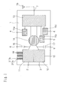
- Figure 1 shows a concept of a block structure of the transmission module for a radio communication apparatus according to the embodiment of the present invention.
- a portable telephone for EDGE of GSM/DCS/PCS the application of the present invention is not limited to this example.
- reference numeral 1 denotes a ceramic board which is an example of the electronic component mounting board of the present invention
- reference numeral 2 denotes a GSM transmission input terminal
- reference numeral 3 denotes a DCS/PCS transmission input terminal
- reference numeral 4 denotes a GSM reception output terminal
- reference numeral 5 denotes a DCS reception output terminal
- reference numeral 6 denotes a PCS reception output terminal
- reference numeral 7 denotes an antenna terminal
- reference numeral 8 denotes a GSM monitor terminal
- reference numeral 9 denotes a DCS/PCS monitor terminal
- reference numeral 10 denotes an EDGE mode switching terminal
- reference terminal 11 denotes a GSM power amplifier IC
- reference numeral 12 denotes a DCS/PCS power amplifier IC
- reference numeral 13 denotes a SP5T GaAs switch IC
- reference numeral 14 denotes a board buried type laminated isolator
- LTCC low-temperature co-fired ceramic board
- Both of a single-layer board and a multilayer board can be used for the board 1.
- a laminated LTCC of different kinds is further preferable in which ceramic sheets having different dielectric constants are laminated.
- materials of the ceramic laminated board 1 for example, it is possible to select forsterite, alumina borosilicate glass, and so on from materials having low dielectric constants (relative dielectric constant of 20 or less) , and Bi-Ca-Nb-O, Ba-Ti-O, [Zr (Mg, Zn, Nb)] TiO 4 + MnO 2 , Ba-Nd-Ti-O, and so on from materials having high dielectric constants (relative dielectric constant larger than 20).
- the GSM power amplifier IC 11 and the DCS/PCS power amplifier IC 12 it is preferable to use a material such as GaAs-FET and InGaP-HBT for the GSM power amplifier IC 11 and the DCS/PCS power amplifier IC 12.
- An FET structure or an HEMT structure is preferable for the GaAs switch IC 13.
- SP5T type other types may be used.
- DP5T and a diplexer may be combined and used.
- the board buried type laminated isolator 14 stabilizes loads of the GSM power amplifier IC 11 and the DCS/PCS power amplifier IC 12 and performs isolation for securing a low-distortion characteristic.
- the built-in laminated filters 15a, 15b, and 15c can be reduced in size by folding a resonator by using via holes (not shown). Besides, it is further preferable that a resonator electrode is formed in a ceramic layer of a high dielectric constant in the ceramic board 1.
- a transmission signal inputted from the GSM transmission input terminal 2 or the DCS/PCS transmission input terminal 3 is amplified to a specified transmission signal output power level by the GSM power amplifier IC 11 or the DCS/PCS power amplifier IC 12.
- a bias point is controlled so that the GSM power amplifier IC 11 or the DCS/PCS power amplifier IC 12 operates as a saturation amplifier of amplifying a GMSK modulation signal or a linear amplifier of amplifying an EDGE signal in response to a control signal applied to the EDGE mode switching terminal 10, and the efficiency and distortion characteristics are set in the most suitable manner in each operation mode.
- the output from each of the power amplifier ICs is inputted to the board buried type laminated isolator 14.
- the coupling capacitor 16 for a GSM monitor and the coupling capacitor 17 for a DCS/PCS monitor are provided to take out just a part of the output from each of the power amplifier ICs and monitor an output power level.
- a directional coupler may be used, since the output from each of the power amplifier ICs is connected to the board buried type laminated isolator 14 and thus the directional property can be secured in the present embodiment, a coupling capacitor with a simple configuration, a smaller area, and lower cost is used.
- the output of the board buried type laminated isolator 14 is inputted to the SP5T GaAs switch IC 13 serving as an antenna switch circuit.
- the GaAs switch IC is used as an antenna switch circuit, a switch circuit using a PIN diode and a switch circuit using an RF-MEMS switch are also applicable.
- the antenna switch circuit directs the output of a transmission signal to the antenna terminal during a transmitting operation, and a reception signal received by the antenna 19 is outputted to each receiving terminal via a receiving filter during a receiving operation.
- a receiving filter a laminated filter, an SAW filter, a BAW filter, and so on are used.
- Members such as the antenna terminal and the receiving filter are constituted integrally with the ceramic laminated board 1 (not shown).
- the SP5T GaAs switch IC 13 serving as an antenna switch circuit
- the ceramic laminated board 1 are integrally constituted.
- the output of the power amplifier is electrically connected to the output of the antenna switch circuit directly or via the board buried type laminated isolator through a transmission line formed on a surface or an inner layer of the ceramic laminated board.
- the size can be remarkably reduced and the cost can be lower at the same time.
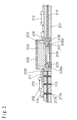
- FIG. 2 is a sectional view showing a main part of the transmission module for a radio communication apparatus according to the present embodiment.
- Reference numeral 201 denotes a ceramic different-kind laminated board
- reference numeral 202 denotes a board buried type laminated isolator
- reference numeral 203 denotes a magnet
- reference numeral 204 denotes a ferrite
- reference numeral 205 denotes an upper yoke
- reference numeral 206 denotes a lower yoke
- reference numeral 207 denotes a lower-surface cavity
- reference numeral 208 denotes a ceramic different-kind laminated board integrated with the board 201
- reference numeral 209 denotes a radiator plate
- reference numeral 210 denotes a power amplifier IC chip
- reference numeral 211 denotes a printed board
- reference numeral 212 denotes a bonding wire
- reference numeral 213 denotes a Ga
- the board buried type laminated isolator 202 is configured so that the upper yoke 205 and the lower yoke 205 sandwich a part of the ceramic different-kind laminated board 201 via the slit 216.
- the magnet 203 is interposed between the upper yoke 205 and one of-the main faces of the ceramic different-kind laminated board 201, and the ferrite 204 is interposed between the lower yoke 206 and the other main face of the ceramic different-kind laminated board 201.
- a metallic body 217a at the center and a cushioning material 217b are placed in the thermal via hole 215.
- the cushioning material 217b is provided between the metallic body 217a and the thermal via hole 215 and is in contact with the inner wall of the thermal via hole 215 and the outer wall of the metallic body 217a.
- a heat transfer body having a two-layer structure of the metallic body 217a and the cushioning material 217b is filled in the thermal via hole 215.
- one end of the heat transfer body is directly connected to the radiator plate 209 so as to tranfer heat and the other end of the heat transfer body is exposed on the other main face of the ceramic different-kind laminated board 201.
- radiator plate 209 and the lower yoke 206 are directly connect so as to transfer heat, the heat radiator 209 and the upper and lower yokes are operated as heat sinkers, and heat generated from the power amplifier IC chip 210, which is placed on the radiator plate 209, is released to the bottom of the module via the heat transfer body connected to the radiator plate 209.
- a ceramic LTCC board is not so high in thermal conductivity, which is the most difficult problem when an LTCC is used in a PA module board or a transmission module board. In the present embodiment, this problem can be solved well by the above configuration.
- an intersecting electrode (not shown) is formed in a thin laminated ceramic layer between the upper surface of the ceramic different-kind laminated board 201 and the lower-surface cavity 207.
- the ferrite 204 is embedded in the lower-surface cavity 207.
- a capacitor electrode connected to the end of the intersecting electrode is formed in a part 208a, which is adjacent to the ferrite 204 and has a large thickness, of the ceramic different-kind laminated board 208 interposed between the upperyoke 205 and the lower yoke 206.
- the present embodiment described the configuration of such a laminated isolator, the present embodiment is not necessarily limited to the above configuration. When the isolator is integrated with the ceramic board, it is understood that the isolator and the board are all included in the scope of the present invention.
- the board buried type laminated isolator 202 and the radiator plate 209 are not always baked concurrently with the ceramic different-kind laminated board 201.
- a composite material is used in which a resin material and a ceramic material are mixed. These materials may be joined to the ceramic laminated board. In this case, the inside of the slit, the lower surface or a surrounding part of the radiator plate, and so on are joined by the composite material. Since the composite material can be usually cured at about 150°, it is possible to prevent cracks and the like caused by a difference in thermal expansion of the radiator plate 209 and the ceramic laminated board 201.
- the printed board 211 is placed on a part of the radiator plate 209 and wire bonding is directly performed by the bonding wire 212 and so on from the ICs including the power amplifier IC chip 210 and the GaAs switch IC chip 213, so that the entry of unnecessary parasitic components can be prevented. Further, gold plating is performed so that an electrode on the printed board 211 can undergo wire bonding.
- silver is normally used as a material of the electrode.
- Figure 4 simply shows an example and the present invention is not limited to this example.
- a point having not been described in Figure 1 and Figure 2 is the slits 216 which are formed in advance to permit the passage of the lower yoke 206.
- the slits 216 are formed partially on the inside of the outer periphery of the lower yoke 206, so that the board buried type laminated isolator 202 and the ceramic laminated board 201 maintain an integrated structure. Therefore, other circuit parts formed on the board buried type laminated isolator 202 and the ceramic laminated board 201 are electrically connected through their continuous parts, thereby preventing the entry of unnecessary parasitic components.
- a slit-shaped through hole 302 corresponding to the thermal via hole 215 is formed on a laminated green sheet 301 made of ceramic that serves as a substrate of the ceramic laminated board 201, baking is performed at about 950°C, which is a first predetermined temperature, so as to obtain the ceramic laminated board 201.
- a baking method it is possible to use both of shrinking baking which freely performs shrinking in the three-dimensional directions and non-shrinking baking which does not permit shrinking in a planar direction.
- the first predetermined temperature required to bake of the green sheet 301 is about 950°C in the case of the ceramic laminated board, this temperature varies according to a metal conductor paste used for the buried type strip line 214 and so on, which is baked concurrently with the green sheet 301, and any temperature is acceptable as long as the temperature is equal to or lower than the melting point of the metal conductor paste.
- the first predetermined temperature is about 1085°.
- the first predetermined temperature is about 962°.
- the first predetermined temperature is set at about 950°C. In short, any temperature is acceptable as long as the ceramic layer substrate of the present invention can be obtained.
- thermosetting is performed at about 150°, which is a second predetermined temperature, and the heat transfer body is placed in the thermal via hole 215.
- a thin plate (or foil) made of a material such as silver, copper, aluminum, and iron is applicable.
- a material such as silver, copper, aluminum, and iron
- silver, copper, and aluminum are preferable.
- iron having a small magnetic resistance is preferable.
- the composite material 304 used as an example of the cushioning material of the present invention for example, it is possible to use a composite material formed by mixing a thermosetting resin made of an epoxy resin and an inorganic filler composed of powder of Al 3 O 3 , MgO, and so on.
- the thermosetting temperature of these composite materials is about 150°.
- a thermosetting resin a phenol resin, a cyanate resin, and so on besides an epoxy resin are also applicable.
- the thermosetting temperature is also about 150° in this case. In short, any temperature can be used as the second predetermined temperature as long as the cushioning material of the present invention is obtained.
- the heat transfer body having a double structure of the metallic body 303 and the composite material 304 can be formed in the ceramic laminated board 201.
- Figure 3(c) shows an example in which a part of the heat transfer body exposed onto the main face of the board and a semiconductor element 305 are directly connected to each other so that thermal conduction is obtained. As shown in Figure 2, the connection may be made via the radiator plate 209.
- the via holes for heat release that have the above-described heat transfer body, it is possible to prevent a crack or a gap that is caused by a difference in thermal expansion coefficient between the ceramic layer board and the metallic body during baking, thereby improving a yield. Further, it is possible to obtain an integrated structure of the ceramic laminated board and the metallic body so as to obtain the via holes with excellent heat release.
- the transmissionmodule for a radio communication apparatus is an example of the electronic component module of the present invention
- the ceramic laminated boards 1 and 201 are examples of the electronic component mounting board or the board of the present invention.
- the GSM power amplifier IC 11, the DCS/PCS power amplifier IC 12, and the SP5T GaAs switch IC are examples of the power amplifiers and the electronic components of the present invention.
- the thermal via holes 18 and 215 are examples of the via holes of the present invention
- the metallic body 303 is an example of the metallic body of the present invention
- the composite material 304 is an example of the cushioning material of the present invention.
- the present invention is not limited to the above-described embodiment.
- the electronic components of the present invention may not be power amplifiers or may not operate in a high-frequency band.
- the electronic components may not be semiconductor components. In short, any components are acceptable as long as connection is made to conduct heat with the heat transfer body.
- the composite material is used as the cushioning material of the present invention, a material of a simple substance is also applicable.
- a material is not limited by its composition as long as the material is higher in thermal conductivity than air to increase the thermal conductivity of the heat transfer body and the material is lower in thermal expansion coefficient than the metallic body or higher in elasticity than the metallic body to prevent a crack on the ceramic layer board when the material is placed into the via hole.
- the above explanation described that the composite material 217b is filled into the gap between the through hole 302 and the metallic body 303.
- the cushoningmaterial of the present invention does not need to be arranged over the gap and may be provided only in a part of the gap.
- the via hole is a slit-like thermal via hole, the shape can be arbitrarily changed.
- the GSM power amplifier IC 11 and the DCS/PCS power amplifier IC 12 that are connected so as to conduct heat with the board buried type laminated isolator 14 are mounted on the electronic component mounting board having the via holes and the heat transfer body of the present invention.
- the electronic component module of the present invention is not limited by the configuration of the board as long as the board buried type laminated isolator is integrated with the power amplifiers in such a manner that a part of the board is included in the isolator.
- a conventional ceramic laminated board which has no via hole and heat transfer body of the present invention may be used.
- the electronic component module of the present invention can be used on both of the transmission side and the reception side of the radio communication apparatus shown in Figure 5, and the radio communication apparatus using this electronic component module is also included in the present invention. Additionally, the module can be used for electronic equipment other than communications equipment.
- an electronic component mounting board which has excellent heat release and a high yield during manufacturing, and a method of manufacturing the board, have a smaller size and lower cost with ease, realize desired characteristics with high reproducibility without making adjustments, and suppress excessive loss, thereby achieving low power consumption.
Landscapes
- Engineering & Computer Science (AREA)
- Microelectronics & Electronic Packaging (AREA)
- Production Of Multi-Layered Print Wiring Board (AREA)
- Cooling Or The Like Of Semiconductors Or Solid State Devices (AREA)
- Structure Of Printed Boards (AREA)
Applications Claiming Priority (2)
| Application Number | Priority Date | Filing Date | Title |
|---|---|---|---|
| JP2002167196 | 2002-06-07 | ||
| JP2002167196 | 2002-06-07 |
Publications (3)
| Publication Number | Publication Date |
|---|---|
| EP1369917A2 true EP1369917A2 (fr) | 2003-12-10 |
| EP1369917A3 EP1369917A3 (fr) | 2006-09-27 |
| EP1369917B1 EP1369917B1 (fr) | 2011-08-03 |
Family
ID=29545883
Family Applications (1)
| Application Number | Title | Priority Date | Filing Date |
|---|---|---|---|
| EP03012908A Expired - Lifetime EP1369917B1 (fr) | 2002-06-07 | 2003-06-06 | Plaque de montage pour composants électroniques, méthode de fabrication associée, module de composants électroniques et appareil de communication |
Country Status (3)
| Country | Link |
|---|---|
| US (1) | US7274570B2 (fr) |
| EP (1) | EP1369917B1 (fr) |
| CN (1) | CN100352317C (fr) |
Cited By (2)
| Publication number | Priority date | Publication date | Assignee | Title |
|---|---|---|---|---|
| EP2059103A4 (fr) * | 2006-08-28 | 2010-08-04 | Univ Tohoku Nat Univ Corp | Dispositif à semi-conducteur et tableau de connexion multicouche |
| US11251146B2 (en) | 2019-04-08 | 2022-02-15 | Infineon Technologies Ag | Semiconductor devices having a non-galvanic connection |
Families Citing this family (9)
| Publication number | Priority date | Publication date | Assignee | Title |
|---|---|---|---|---|
| JP4185499B2 (ja) | 2005-02-18 | 2008-11-26 | 富士通マイクロエレクトロニクス株式会社 | 半導体装置 |
| US7583506B1 (en) * | 2005-10-14 | 2009-09-01 | The Boeing Company | Multi operational system apparatus and method |
| US8138859B2 (en) * | 2008-04-21 | 2012-03-20 | Formfactor, Inc. | Switch for use in microelectromechanical systems (MEMS) and MEMS devices incorporating same |
| CN103283152B (zh) | 2011-01-06 | 2015-06-24 | 株式会社村田制作所 | 高频模块 |
| JPWO2017061324A1 (ja) * | 2015-10-09 | 2018-03-01 | 日立金属株式会社 | 多層セラミック基板の製造方法 |
| CN106455298B (zh) * | 2016-10-31 | 2023-08-04 | 成都八九九科技股份有限公司 | 一种内置有磁片的微波电路复合基板 |
| WO2018101112A1 (fr) * | 2016-11-30 | 2018-06-07 | 株式会社村田製作所 | Tableau de connexions, module coupleur et dispositif de communication |
| CN107222983B (zh) * | 2017-06-09 | 2019-05-03 | 深圳市景旺电子股份有限公司 | 一种内嵌AlN陶瓷绝缘散热模块的PCB板及制作方法 |
| CN111180843B (zh) * | 2020-01-07 | 2021-11-02 | 中国电子科技集团公司第五十五研究所 | 一种mems微带环形器及其制备方法 |
Family Cites Families (22)
| Publication number | Priority date | Publication date | Assignee | Title |
|---|---|---|---|---|
| JPS5326761A (en) * | 1976-08-26 | 1978-03-13 | Babcock Hitachi Kk | Injecting device for reducing agent for nox |
| JPS5448167A (en) * | 1977-09-24 | 1979-04-16 | Nec Corp | High-density circuit package |
| GB8304890D0 (en) * | 1983-02-22 | 1983-03-23 | Smiths Industries Plc | Chip-carrier substrates |
| JPS63274196A (ja) * | 1987-05-06 | 1988-11-11 | Mitsubishi Electric Corp | 金属芯印刷配線板 |
| US5506755A (en) * | 1992-03-11 | 1996-04-09 | Kabushiki Kaisha Toshiba | Multi-layer substrate |
| JPH10326961A (ja) | 1997-05-23 | 1998-12-08 | Hitachi Aic Inc | 配線基板のバンプ形成方法 |
| US5920458A (en) * | 1997-05-28 | 1999-07-06 | Lucent Technologies Inc. | Enhanced cooling of a heat dissipating circuit element |
| JP2950290B2 (ja) * | 1997-06-27 | 1999-09-20 | 日本電気株式会社 | 高周波集積回路装置およびその製造方法 |
| US6016005A (en) * | 1998-02-09 | 2000-01-18 | Cellarosi; Mario J. | Multilayer, high density micro circuit module and method of manufacturing same |
| TW473882B (en) * | 1998-07-06 | 2002-01-21 | Hitachi Ltd | Semiconductor device |
| JP3677403B2 (ja) * | 1998-12-07 | 2005-08-03 | パイオニア株式会社 | 発熱素子の放熱構造 |
| SE513786C2 (sv) * | 1999-03-09 | 2000-11-06 | Ericsson Telefon Ab L M | Metod för framställning av mönsterkort samt anordning för värmeavledning framställt enligt metoden |
| TW424314B (en) * | 1999-07-09 | 2001-03-01 | Taiwan Semiconductor Mfg | Interconnection lines for improving thermal conductivity in integrated circuits and method for fabricating the same |
| US6597259B1 (en) * | 2000-01-11 | 2003-07-22 | James Michael Peters | Selective laminated filter structures and antenna duplexer using same |
| WO2001069710A1 (fr) * | 2000-03-15 | 2001-09-20 | Matsushita Electric Industrial Co., Ltd. | Composant electronique multicouche, duplexeur d'antenne multicouche, et appareil de communication |
| US6477054B1 (en) * | 2000-08-10 | 2002-11-05 | Tektronix, Inc. | Low temperature co-fired ceramic substrate structure having a capacitor and thermally conductive via |
| US6462950B1 (en) * | 2000-11-29 | 2002-10-08 | Nokia Mobile Phones Ltd. | Stacked power amplifier module |
| JP2002261643A (ja) * | 2001-02-28 | 2002-09-13 | Tdk Corp | 無線通信モジュール |
| US6414847B1 (en) * | 2001-04-09 | 2002-07-02 | Agilent Technologies, Inc. | Integral dielectric heatspreader |
| US7023301B2 (en) * | 2001-05-16 | 2006-04-04 | Matsushita Electric Industrial Co., Ltd. | Laminated filter with a single shield conductor, integrated device, and communication apparatus |
| US6980439B2 (en) * | 2001-12-27 | 2005-12-27 | Intel Corporation | EMI shield for transceiver |
| US6671176B1 (en) * | 2002-06-27 | 2003-12-30 | Eastman Kodak Company | Method of cooling heat-generating electrical components |
-
2003
- 2003-06-04 CN CNB031409237A patent/CN100352317C/zh not_active Expired - Fee Related
- 2003-06-06 EP EP03012908A patent/EP1369917B1/fr not_active Expired - Lifetime
- 2003-06-09 US US10/457,247 patent/US7274570B2/en not_active Expired - Fee Related
Cited By (3)
| Publication number | Priority date | Publication date | Assignee | Title |
|---|---|---|---|---|
| EP2059103A4 (fr) * | 2006-08-28 | 2010-08-04 | Univ Tohoku Nat Univ Corp | Dispositif à semi-conducteur et tableau de connexion multicouche |
| US7977796B2 (en) | 2006-08-28 | 2011-07-12 | National University Corporation Tohoku University | Semiconductor device and multilayer wiring board |
| US11251146B2 (en) | 2019-04-08 | 2022-02-15 | Infineon Technologies Ag | Semiconductor devices having a non-galvanic connection |
Also Published As
| Publication number | Publication date |
|---|---|
| CN100352317C (zh) | 2007-11-28 |
| US20040240183A1 (en) | 2004-12-02 |
| CN1468046A (zh) | 2004-01-14 |
| EP1369917A3 (fr) | 2006-09-27 |
| US7274570B2 (en) | 2007-09-25 |
| EP1369917B1 (fr) | 2011-08-03 |
Similar Documents
| Publication | Publication Date | Title |
|---|---|---|
| US6456172B1 (en) | Multilayered ceramic RF device | |
| US6998708B2 (en) | Millimeter wave (MMW) transceiver module with transmitter, receiver and local oscillator frequency multiplier surface mounted chip set | |
| KR100674793B1 (ko) | 세라믹 적층 소자 | |
| US7701728B2 (en) | Electronic component module and radio comunications equipment | |
| US7089032B2 (en) | Radio transmitting/receiving device | |
| US7149496B2 (en) | High-frequency module and radio communication apparatus | |
| EP1094538A2 (fr) | Dispositif HF multicouche céramique | |
| US7808796B2 (en) | Electronic component module and method for manufacturing the same | |
| US8952846B2 (en) | Electronic apparatus, method of making the same, and transceiving device | |
| CN101110404A (zh) | 混合集成电路器件及其制造方法和电子装置 | |
| EP1369917B1 (fr) | Plaque de montage pour composants électroniques, méthode de fabrication associée, module de composants électroniques et appareil de communication | |
| JP2005026368A (ja) | 放熱用ビアホールを備えた積層基板および該基板を用いたパワーアンプモジュール | |
| JP2005191435A (ja) | 放熱ビア付き基板およびパワーアンプモジュール | |
| JP2002111218A (ja) | セラミック積層デバイス | |
| JP4050186B2 (ja) | 電子部品実装基板の製造方法 | |
| US7193862B2 (en) | Ceramic laminated device, communication equipment and method of manufacturing ceramic laminated device | |
| JP3510971B2 (ja) | 高周波用電力増幅器 | |
| CN100378967C (zh) | 陶瓷封装及其制造方法 | |
| JP2004304435A (ja) | マルチバンド無線通信モジュールおよびマルチバンド無線通信端末機 | |
| JPH09167825A (ja) | 複合マイクロ波集積回路 | |
| JP3766621B2 (ja) | 入出力端子および半導体素子収納用パッケージ | |
| US20060236533A1 (en) | Bonding arrangement and method for LTCC circuitry | |
| JP4502543B2 (ja) | セラミック端子および半導体素子収納用パッケージ | |
| JP4514595B2 (ja) | 入出力端子ならびにこれを用いた電子部品収納用パッケージおよび電子装置 | |
| CN119030562A (zh) | 高频模块和通信装置 |
Legal Events
| Date | Code | Title | Description |
|---|---|---|---|
| PUAI | Public reference made under article 153(3) epc to a published international application that has entered the european phase |
Free format text: ORIGINAL CODE: 0009012 |
|
| AK | Designated contracting states |
Kind code of ref document: A2 Designated state(s): AT BE BG CH CY CZ DE DK EE ES FI FR GB GR HU IE IT LI LU MC NL PT RO SE SI SK TR |
|
| AX | Request for extension of the european patent |
Extension state: AL LT LV MK |
|
| PUAL | Search report despatched |
Free format text: ORIGINAL CODE: 0009013 |
|
| AK | Designated contracting states |
Kind code of ref document: A3 Designated state(s): AT BE BG CH CY CZ DE DK EE ES FI FR GB GR HU IE IT LI LU MC NL PT RO SE SI SK TR |
|
| AX | Request for extension of the european patent |
Extension state: AL LT LV MK |
|
| 17P | Request for examination filed |
Effective date: 20061211 |
|
| 17Q | First examination report despatched |
Effective date: 20070124 |
|
| AKX | Designation fees paid |
Designated state(s): DE GB |
|
| RAP1 | Party data changed (applicant data changed or rights of an application transferred) |
Owner name: PANASONIC CORPORATION |
|
| GRAP | Despatch of communication of intention to grant a patent |
Free format text: ORIGINAL CODE: EPIDOSNIGR1 |
|
| GRAS | Grant fee paid |
Free format text: ORIGINAL CODE: EPIDOSNIGR3 |
|
| GRAA | (expected) grant |
Free format text: ORIGINAL CODE: 0009210 |
|
| AK | Designated contracting states |
Kind code of ref document: B1 Designated state(s): DE GB |
|
| REG | Reference to a national code |
Ref country code: GB Ref legal event code: FG4D |
|
| REG | Reference to a national code |
Ref country code: DE Ref legal event code: R096 Ref document number: 60337885 Country of ref document: DE Effective date: 20110929 |
|
| PLBE | No opposition filed within time limit |
Free format text: ORIGINAL CODE: 0009261 |
|
| STAA | Information on the status of an ep patent application or granted ep patent |
Free format text: STATUS: NO OPPOSITION FILED WITHIN TIME LIMIT |
|
| 26N | No opposition filed |
Effective date: 20120504 |
|
| REG | Reference to a national code |
Ref country code: DE Ref legal event code: R097 Ref document number: 60337885 Country of ref document: DE Effective date: 20120504 |
|
| PGFP | Annual fee paid to national office [announced via postgrant information from national office to epo] |
Ref country code: GB Payment date: 20140604 Year of fee payment: 12 |
|
| PGFP | Annual fee paid to national office [announced via postgrant information from national office to epo] |
Ref country code: DE Payment date: 20140603 Year of fee payment: 12 |
|
| REG | Reference to a national code |
Ref country code: DE Ref legal event code: R119 Ref document number: 60337885 Country of ref document: DE |
|
| GBPC | Gb: european patent ceased through non-payment of renewal fee |
Effective date: 20150606 |
|
| PG25 | Lapsed in a contracting state [announced via postgrant information from national office to epo] |
Ref country code: DE Free format text: LAPSE BECAUSE OF NON-PAYMENT OF DUE FEES Effective date: 20160101 Ref country code: GB Free format text: LAPSE BECAUSE OF NON-PAYMENT OF DUE FEES Effective date: 20150606 |