EP1372041A2 - Réglage d'un appareil pour l'exposition d'un dispositif semiconducteur - Google Patents
Réglage d'un appareil pour l'exposition d'un dispositif semiconducteur Download PDFInfo
- Publication number
- EP1372041A2 EP1372041A2 EP03253658A EP03253658A EP1372041A2 EP 1372041 A2 EP1372041 A2 EP 1372041A2 EP 03253658 A EP03253658 A EP 03253658A EP 03253658 A EP03253658 A EP 03253658A EP 1372041 A2 EP1372041 A2 EP 1372041A2
- Authority
- EP
- European Patent Office
- Prior art keywords
- wafer
- height information
- exposure
- height
- information
- Prior art date
- Legal status (The legal status is an assumption and is not a legal conclusion. Google has not performed a legal analysis and makes no representation as to the accuracy of the status listed.)
- Withdrawn
Links
Images


Classifications
-
- G—PHYSICS
- G03—PHOTOGRAPHY; CINEMATOGRAPHY; ANALOGOUS TECHNIQUES USING WAVES OTHER THAN OPTICAL WAVES; ELECTROGRAPHY; HOLOGRAPHY
- G03F—PHOTOMECHANICAL PRODUCTION OF TEXTURED OR PATTERNED SURFACES, e.g. FOR PRINTING, FOR PROCESSING OF SEMICONDUCTOR DEVICES; MATERIALS THEREFOR; ORIGINALS THEREFOR; APPARATUS SPECIALLY ADAPTED THEREFOR
- G03F9/00—Registration or positioning of originals, masks, frames, photographic sheets or textured or patterned surfaces, e.g. automatically
- G03F9/70—Registration or positioning of originals, masks, frames, photographic sheets or textured or patterned surfaces, e.g. automatically for microlithography
- G03F9/7003—Alignment type or strategy, e.g. leveling, global alignment
- G03F9/7023—Aligning or positioning in direction perpendicular to substrate surface
- G03F9/7026—Focusing
-
- G—PHYSICS
- G03—PHOTOGRAPHY; CINEMATOGRAPHY; ANALOGOUS TECHNIQUES USING WAVES OTHER THAN OPTICAL WAVES; ELECTROGRAPHY; HOLOGRAPHY
- G03F—PHOTOMECHANICAL PRODUCTION OF TEXTURED OR PATTERNED SURFACES, e.g. FOR PRINTING, FOR PROCESSING OF SEMICONDUCTOR DEVICES; MATERIALS THEREFOR; ORIGINALS THEREFOR; APPARATUS SPECIALLY ADAPTED THEREFOR
- G03F9/00—Registration or positioning of originals, masks, frames, photographic sheets or textured or patterned surfaces, e.g. automatically
- G03F9/70—Registration or positioning of originals, masks, frames, photographic sheets or textured or patterned surfaces, e.g. automatically for microlithography
- G03F9/7003—Alignment type or strategy, e.g. leveling, global alignment
- G03F9/7007—Alignment other than original with workpiece
- G03F9/7011—Pre-exposure scan; original with original holder alignment; Prealignment, i.e. workpiece with workpiece holder
-
- G—PHYSICS
- G03—PHOTOGRAPHY; CINEMATOGRAPHY; ANALOGOUS TECHNIQUES USING WAVES OTHER THAN OPTICAL WAVES; ELECTROGRAPHY; HOLOGRAPHY
- G03F—PHOTOMECHANICAL PRODUCTION OF TEXTURED OR PATTERNED SURFACES, e.g. FOR PRINTING, FOR PROCESSING OF SEMICONDUCTOR DEVICES; MATERIALS THEREFOR; ORIGINALS THEREFOR; APPARATUS SPECIALLY ADAPTED THEREFOR
- G03F9/00—Registration or positioning of originals, masks, frames, photographic sheets or textured or patterned surfaces, e.g. automatically
- G03F9/70—Registration or positioning of originals, masks, frames, photographic sheets or textured or patterned surfaces, e.g. automatically for microlithography
- G03F9/7003—Alignment type or strategy, e.g. leveling, global alignment
- G03F9/7023—Aligning or positioning in direction perpendicular to substrate surface
- G03F9/7034—Leveling
-
- G—PHYSICS
- G03—PHOTOGRAPHY; CINEMATOGRAPHY; ANALOGOUS TECHNIQUES USING WAVES OTHER THAN OPTICAL WAVES; ELECTROGRAPHY; HOLOGRAPHY
- G03F—PHOTOMECHANICAL PRODUCTION OF TEXTURED OR PATTERNED SURFACES, e.g. FOR PRINTING, FOR PROCESSING OF SEMICONDUCTOR DEVICES; MATERIALS THEREFOR; ORIGINALS THEREFOR; APPARATUS SPECIALLY ADAPTED THEREFOR
- G03F9/00—Registration or positioning of originals, masks, frames, photographic sheets or textured or patterned surfaces, e.g. automatically
- G03F9/70—Registration or positioning of originals, masks, frames, photographic sheets or textured or patterned surfaces, e.g. automatically for microlithography
- G03F9/7003—Alignment type or strategy, e.g. leveling, global alignment
- G03F9/7046—Strategy, e.g. mark, sensor or wavelength selection
Definitions
- the present invention relates to a semiconductor exposure apparatus, control method therefor, and semiconductor device manufacturing method.
- Typical proximity exposure apparatuses which perform exposure by bringing a mask (master) and a substrate such as a wafer or the like close to each other include an X-ray exposure apparatus.
- an X-ray exposure apparatus using an SR light source is disclosed in Japanese Patent Laid-Open No. 2-100311.
- Fig. 1 is a schematic view showing a general arrangement of a conventional X-ray exposure apparatus of this type.
- a mask 101 with a patterned mask membrane 102 is held by a mask chuck 104 mounted on a mask stage base 106 and aligned with respect to an X-ray optical path.
- a wafer 103 is held by a wafer chuck 105, faces the mask 101, and is spaced apart from the mask 101 by an infinitesimal distance, i.e., arranged close to the mask 101.
- the wafer chuck 105 is mounted on a fine adjustment stage 113 used to align the mask 101 and wafer 103.
- the wafer chuck 105 and fine adjustment stage 113 are mounted on a coarse adjustment stage 112 used for movement between shots so that the irradiation region of X-ray beams can be sequentially stepped over a plurality of field angles of exposure of the wafer 103.
- the coarse adjustment stage 112 is guided by a stage base 107.
- An alignment scope 108 is designed to measure the amount of shift between the mask 101 and the wafer 103 in their alignment and is mounted on an alignment stage 109.
- the alignment stage 109 is mounted on the mask stage base 106 and is used to move alignment light emitted from the alignment scope 108 to an alignment mark position (not shown) formed on the mask membrane 102.
- the mask membrane 102 and wafer 103 are spaced apart from each other by an infinitesimal distance of 10 to 30 ⁇ m to face each other, and exposure (proximity exposure) is performed using the step & repeat scheme, in which exposure of the wafer 103 to the pattern on the mask membrane 102 is repeated a plurality of number of times.
- the X-ray exposure apparatus performs exposure for a predetermined number of shots of the wafer 103 by repeating the steps (4) to (6) in the same manner.
- a conventional X-ray exposure apparatus does not take any measurement error induced by wafer process into consideration in gap measurement, posing the following problems.
- measurement errors induced by the process include ones due to unevenness of the wafer surface (e.g., unevenness of the pattern, defects due to a foreign substance, roughness of the wafer surface, unevenness of the reverse surface of the photoresist applied to the wafer surface, and the like). Additionally, these problems are not limited to the proximity scheme. For example, similar problems arise in, e.g., AF measurement by reduction projection exposure using an excimer laser as a light source.
- AF measurement is performed by diagonally projecting light onto the wafer surface and detecting its reflection light as the height of the wafer surface using a CCD or the like.
- the wafer process induces measurement errors.
- a preceding wafer is used to perform pre-exposure, thereby determining the best focus from the exposure result, for each wafer layer (exposure step).
- any measurement error is reflected as an offset value in AF measurement or AF setting on the basis of the best focus.
- Embodiments of the present invention seek to reduce the above-mentioned problems, and to increase the productivity of devices.
- a semiconductor exposure apparatus for tranfering a pattern of a master onto a wafer, comprising a measuring unit which measures wafer height information, and an adjustment unit which adjusts a position of the master in a direction of height and/or a position of the wafer in a direction of height on the basis of wafer height information in a preceding exposure step and wafer height information in a current exposure step.
- the apparatus preferably further comprises a processor which stores the wafer height information in a memory.
- the processor preferably associates the wafer height information with identification information for identifying the wafer to store the associated information in the memory.
- the processor preferably reads out the wafer height information in the preceding exposure step from the memory on the basis of the identification information.
- the processor preferably stores in the memory at least one of a height of the wafer from a predetermined reference position and an amount of adjustment by the adjustment unit as the wafer height information.
- the apparatus preferably further comprises a controller which outputs a command value for controlling the adjustment unit on the basis of the wafer height information in the preceding exposure step and the wafer height information in the current exposure step.
- the apparatus preferably further comprises a controller which has a function of, when a difference between the wafer height information in the preceding exposure step and the wafer height information in the current exposure step is not less than a predetermined value, stopping operation of the apparatus.
- the controller preferably performs an operation of adding the wafer height information in the preceding exposure step and the wafer height information in the current exposure step in a predetermined ratio, and the adjustment unit preferably adjusts the position of the master in the direction of height and/or the position of the wafer in the direction of height on the basis of the operation result obtained by the controller.
- the controller preferably has an evaluation function for changing the ratio in accordance with each exposure step on the basis of the wafer height information in the preceding exposure step and the wafer height information in the current exposure step.
- the adjustment unit preferably adjusts the position of the master in the direction of height and/or the position of the wafer in the direction of height such that a distance between the master and the wafer equals a predetermined infinitesimal distance.
- the adjustment unit preferably adjusts the position of the master in the direction of height and/or the position of the wafer in the direction of height such that the position of the wafer in the direction of height equals a focus position of exposure light.
- a method of controlling an exposure apparatus for transfering a pattern of a master onto a wafer comprising a measurement step of measuring wafer height information, and an adjustment step of adjusting a position of the master in a direction of height and/or a position of the wafer in a direction of height on the basis of wafer height information in a preceding exposure step and wafer height information in a current exposure step.
- a semiconductor device manufacturing method comprising a coating step of coating a substrate with a photosensitive agent, an exposure step of transferring a pattern onto the substrate coated with the photosensitive agent in the coating step using a semiconductor exposure apparatus as defined in any one of claims 1 to 11, and a development step of developing the photosensitive agent on the substrate, onto which the pattern is transferred in the exposure step.
- Fig. 2 is a schematic view showing part of the arrangement of a semiconductor exposure apparatus according to a preferred embodiment of the present invention.
- a measuring unit 201 measures the positions of the mask 1 and/or the wafer 3 in their respective directions of height and stores the measurement result in a memory 202.
- the memory 202 may be provided in or outside the semiconductor exposure apparatus.
- the above-mentioned measurement result may temporarily be stored in a memory within the semiconductor exposure apparatus and then transferred to a memory provided outside the semiconductor exposure apparatus.
- Adjustment units 203 have a function of adjusting the positions of the mask 1 and/or the wafer 3 in their respective directions of height.
- the adjustment unit 203 on the wafer side can comprise, e.g., a wafer chuck which holds the wafer and/or a Z tilt stage which moves the wafer in its direction of height.
- the adjustment unit 203 on the mask side can comprise, e.g., a mask chuck which holds the mask and/or a mask stage which moves the mask in its direction of height.
- the adjustment units 203 adjust the positions of the mask 1 and/or the wafer 3 in their respective directions of height on the basis of the wafer height information in the current exposure step obtained by the measuring unit 201 and that in past exposure steps stored in, e.g., the memory 202.
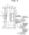
- Fig. 3 is a view for explaining exposure operation by global alignment in the semiconductor exposure apparatus according to the preferred embodiment of the present invention.
- the mask 1 with a mask membrane 2 on which a pattern is formed is held by a mask stage 4 with a mask chuck mounted on a mask stage base 6.
- the mask 1 is aligned with respect to an X-ray optical path.
- the wafer 3 serving as a substrate, which faces the mask 1 and is spaced apart from the mask 1 by an infinitesimal distance, i.e., arranged close to the mask 1, is held by a wafer chuck 5.
- the wafer chuck 5 is mounted on a Z tilt stage 13 used to align the mask 1 and wafer 3.
- the wafer chuck 5 and Z tilt stage 13 are mounted on an X-Y stage 12 used for movement between shots so that the irradiation region of X-ray beams can be sequentially stepped over a plurality of field angles of exposure of the wafer 3.
- the X-Y stage 12 is guided by a stage surface plate 7.
- An alignment scope 8 is designed to measure the amount of shift between the mask 1 and the wafer 3 in their alignment and is mounted on an alignment stage 9.
- the alignment stage 9 is designed to align the alignment scope 8 such that alignment light emitted from the alignment scope 8 strikes an alignment mark (not shown) formed on the mask membrane 2 and is mounted on the mask stage base 6.
- a wafer height sensor 10 is designed to measure the position of the wafer in its direction of height and inform a controller 304 of the height information of the wafer.
- the wafer height sensor 10 is mounted on the mask stage base 6.
- a mask height sensor 11 is designed to measure the position of the mask in its direction of height and is mounted on the X-Y stage 12. Though Fig. 3 shows only one wafer height sensor 10, the present invention is not limited to this.
- a plurality of wafer height sensors may be provided.
- a processor 301 has a function of managing for each wafer the wafer height information at the time of exposure in the preceding layers (exposure steps).
- the processor 301 can manage the wafer height information by, e.g., having a function of associating the height information of each wafer with identification information for identifying the wafer to store the associated information in a memory (not shown) and reading out the wafer height information in the preceding exposure steps from the memory on the basis of the identification information.
- the controller 304 outputs command values (e.g., a Z tilt correction amount for the Z tilt stage 13) for controlling an adjustment unit (e.g., the Z tilt stage 13) on the basis of the wafer height information in the preceding exposure steps which the processor 301 manages within the memory (not shown) and the current wafer height information obtained by the wafer height sensor 10.
- command values e.g., a Z tilt correction amount for the Z tilt stage 13
- an adjustment unit e.g., the Z tilt stage 13
- a console can be provided with the functions to be assigned to the processor 301 or controller 304.
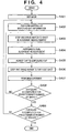
- Fig. 4 is a flow chart of exposure operation by global alignment using the semiconductor exposure apparatus shown in Fig. 3.
- n be the number of the current layer (exposure step) at this time
- (n - 1) be the number of the immediately preceding layer (exposure step).
- step S401 the mask 1 is set at a predetermined position. More specifically, the mask 1 is first conveyed to the mask chuck 4 and held by the mask chuck 4. Then, the mask height sensor 11 measures the position of the mask 1 in its direction of height, and the mask stage 4 aligns the mask 1 at the predetermined position with respect to a predetermined reference position (apparatus reference) on the basis of the measurement result. Note that since the apparatus reference is a virtual reference, it is not shown in Fig. 3.
- the X-Y stage 12 is driven such that a reference mark base (not shown) mounted on the X-Y stage 12 is located below the mask membrane 2.
- the alignment stage 9 adjusts the position of the alignment scope 8 such that alignment light emitted from the alignment scope 8 passes through an alignment mark on the mask membrane 2, is reflected on the reference mark base, and returns to the alignment scope 8.
- step S402 the wafer height sensor 10 performs mapping of the wafer height information. More specifically, the wafer chuck 5 first holds the loaded wafer 3. The wafer height sensor 10 measures the position of the wafer 3 in its direction of height and performs mapping of the height from the apparatus reference. At this stage, the positional relationship between the mask 1 or wafer 3 and the apparatus reference is obtained, and gap measurement ends. Mapping includes the following steps. The controller 304 determines the Z tilt correction amount of the Z tilt stage 13 in gap setting on the basis of the nth wafer height information obtained by the wafer height sensor 10 and preceding height information up to the (n - 1)th height information of the same wafer already obtained by the processor 301.
- This determination may be performed by, e.g., adding the nth wafer height information and the preceding height information up to the (n - 1)th wafer height information in a predetermined ratio.
- the controller 304 calculates a difference (change in flatness) between the nth wafer height information and the preceding height information up to the (n - 1)th wafer height information. If the difference is equal to or more than a predetermined value, the operation of the apparatus is preferably stopped. In this case, a foreign substance or the like may be present on the reverse surface of the wafer 3.
- the user preferably performs maintenance such as cleaning of the wafer chuck 5 and the like.
- step S403 the X-Y stage 12 drives the wafer 3 such that a predetermined shot of the wafer 3 is located under the mask membrane 2 in global alignment measurement. Additionally, at this time, the Z tilt stage 13 preferably adjusts the position of the wafer 3 in the direction of height such that the gap equals the alignment gap (e.g., 25 ⁇ m).
- the alignment gap e.g. 25 ⁇ m
- step S404 the X-Y stage 12 aligns the wafer 3 at each shot position in global alignment measurement while keeping the alignment gap, and global alignment is performed in this state.
- step S405 after the global alignment measurement, the Z tilt stage 13 adjusts the position of the wafer 3 in the direction of height such that the gap equals the exposure gap (e.g., 10 ⁇ m).
- the exposure gap e.g. 10 ⁇ m
- step S406 the X-Y stage 12 aligns the wafer 3 at a predetermined shot position on the basis of the measurement result of the global alignment measurement while keeping the exposure gap.
- step S407 the semiconductor exposure apparatus performs exposure.
- step S408 the controller 304 of the semiconductor exposure apparatus determines whether exposure is completed for a predetermined number of shots. If exposure is completed for the predetermined number of shots (YES in step S408), the flow advances to step S409. If exposure is not completed for the predetermined number of shots (NO in step 5408), the flow returns to step S406, and exposure processing is performed for the next shot.
- step S409 the controller 304 of the semiconductor exposure apparatus determines whether exposure is completed for a predetermined number of shots in the current exposure step. If exposure is completed for the predetermined number of shots (YES in step S409), the exposure processing ends. If exposure is not completed for the predetermined number of shots (NO in step S409), the flow returns to step S402, and exposure processing is performed for the next shot.
- the controller 304 determines the Z tilt correction amount by adding the nth wafer height information and the preceding height information up to the (n - 1)th wafer height information in a predetermined ratio.
- the controller 304 may have an evaluation function for changing the ratio in accordance with each exposure step on the basis of the wafer height information in the preceding exposure steps and that in the current exposure step.
- an evaluation function may be prepared to change the ratio of the nth wafer height information and the preceding height information up to the (n - 1)th wafer height information in accordance with each layer (exposure step).
- any of the first height information to the (n - 1)th height information of the wafer may be employed.
- the (n -1)th wafer height information which is closest to the height information of the nth wafer to be exposed, is preferably employed.
- the thickness of the layer, that of the resist, and the like in each of the first to the (n - 1)th wafers are known, any of the first wafer height information to the (n - 1)th wafer height information may be employed.
- the known thickness information of each layer and resist may preferably be added to the wafer height information to manage the resultant information in a memory (not shown) by the processor 301.
- the wafer height information is not limited to the height information using the apparatus reference.
- the correction amount in the Z tilt stage 13 may represent the wafer height information and be managed.
- the controller 304 may convert the nth wafer height information to the Z tilt correction amount and add the obtained Z tilt correction amount to the Z tilt correction amount up to the (n - 1)th Z tilt correction amount in a predetermined ratio.
- the wafer height sensor 10 measures the height of the wafer 3 and then performs mapping of the height from the apparatus reference.
- the present invention is not limited to this.
- this embodiment can be applied to a case wherein AF measurement is performed by die-by-die.
- the wafer height sensor 10 is not necessarily used.
- the alignment scope 8 preferably directly performs AF measurement.
- a console (not shown) can be provided with the functions to be assigned to the processor 301 or controller 304, as described above.
- this embodiment is not limited to this.
- a computer other than the console may have these functions.
- the controller 304 determines whether the difference between the nth wafer height information and wafer height information up to the (n - 1)th wafer height information is equal to or more than a predetermined value in the processing flow of the wafer height information and the Z tilt correction amount information in Fig. 3.
- the present invention is not limited to this.
- another controller connected to the controller 304 may have this determination function.
- the controller 304 may determine the Z tilt correction amount after this determination.
- the controller 304 may determine the Z tilt correction amount only if the difference between the nth wafer height information and the wafer height information up to the (n - 1)th wafer height information is equal to or less than the predetermined value.
- the wafer height information is described in consideration of AF measurement by mapping or die-by-die.
- this embodiment is not limited to this.
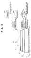
- this embodiment can be applied to a case wherein focus alignment is performed simultaneously with AF measurement in real time, as shown in Fig. 5.
- Fig. 5 shows operation obtained by adding the characteristic features of the present embodiment to AF measurement by general reduction projection exposure.
- the wafer 3 serving as a substrate is held by the wafer chuck 5.
- the wafer chuck 5 is mounted on the Z tilt stage 13 used to align the wafer 3.
- the wafer chuck 5 and Z tilt stage 13 are mounted on the X-Y stage 12 used for movement between shots so that the irradiation region of exposure light can be sequentially stepped or scanned over a plurality of field angles of exposure of the wafer 3.
- the X-Y stage 12 is guided by the stage surface plate 7.
- a light-projecting unit 14 diagonally projects light onto the surface of the wafer, and a light-receiving unit 15 receives light reflected by the wafer 3.
- the light-receiving unit 15 incorporates a CCD or the like and calculates the height of the wafer 3 from the barycentric position of the reflected light.
- the device to be incorporated in the light-receiving unit 15 is not limited to the CCD.
- a PSD may be incorporated instead.
- the light-projecting unit 14 preferably projects light using an LD, LED, or the like.
- the processor 301 manages for each wafer the wafer height information obtained when the preceding layers (exposure steps) are exposed.
- the processor 301 manages the wafer height information by, e.g., having a function of associating the height information of each wafer with identification information for identifying the wafer to store the associated information in a memory (not shown) and reading out the wafer height information in the preceding exposure step from the memory on the basis of the identification information.
- Fig. 5 shows only one set of the light-projecting unit 14 and the light-receiving unit 15, the semiconductor exposure apparatus may have a plurality of sets.
- the controller 304 outputs command values (e.g., a Z tilt correction amount for the Z tilt stage 13) for controlling an adjustment unit (e.g., the Z tilt stage 13) on the basis of the wafer height information in the preceding exposure step managed by the processor 301 and the current wafer height information obtained by the light-receiving unit 15.
- command values e.g., a Z tilt correction amount for the Z tilt stage 13
- an adjustment unit e.g., the Z tilt stage 13
- a console (not shown) can be provided with the functions to be assigned to the processor 301 or controller 304.
- the light-projecting unit 14 and light-receiving unit 15 measure the height of the first shot or its vicinity of the wafer 3.
- the controller 304 determines the Z tilt correction amount of the Z tilt stage 13 on the basis of the obtained wafer height information and, e.g., wafer height information up to the (n - 1)th height information of the same wafer already obtained by the processor 301.
- the controller 304 determines the Z tilt correction amount by adding the nth wafer height information and, e.g., the wafer height information up to the (n - 1)th wafer height information of the same wafer in a predetermined ratio.
- the controller 304 may have an evaluation function for changing the ratio in accordance with each exposure step on the basis of the wafer height information in the preceding exposure steps and that in the current exposure step.
- an evaluation function may be prepared to change the ratio of the nth wafer height information and the wafer height information up to the (n - 1)th wafer height information in accordance with each layer (exposure step).
- any of the first wafer height information to the (n - 1)th wafer height information may be employed.
- the correction amount in the Z tilt stage 13 may represent the wafer height information and be managed.
- the controller 304 calculates a difference (change in flatness) between the nth wafer height information and the wafer height information up to the (n - 1)th wafer height information. If the difference is equal to or more than a predetermined value, the operation of the apparatus is preferably stopped. In this case, a foreign substance or the like may be present on the reverse surface of the wafer 3. The user preferably performs maintenance including cleaning of the wafer chuck 5.
- a console (not shown) can be provided with the functions to be assigned to the processor 301 or controller 304, as described above.
- this embodiment is not limited to this.
- a computer other than the console may have these functions.
- the controller 304 determines whether the difference between the nth wafer height information and the wafer height information up to the (n - 1)th wafer height information is equal to or more than a predetermined value in the flow of the wafer height information and the Z tilt correction amount information in Fig. 5.
- another controller connected to the controller 304 may have this determination function.
- the controller 304 may determine the Z tilt correction amount after this determination.
- the controller 304 may determine the Z tilt correction amount only if the difference between the nth wafer height information and the wafer height information up to the (n - 1)th wafer height information is equal to or less than the predetermined value.
- the first embodiment has described that all the layers (exposure steps) are exposed by one exposure apparatus.
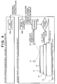
- an arrangement which supports the mix & match scheme will be described with reference to Fig. 6.
- this embodiment can also be applied to the exposure apparatus using the mapping scheme described with reference to Fig. 3.
- this embodiment can be applied to the mix & match scheme, which combines the mapping scheme, die-by-die scheme, and real-time scheme.
- n be the number of a layer (exposure step) to be exposed this time
- (n - 1) be the number of an immediately preceding exposed layer (exposure step).
- a wafer 3 serving as a substrate is held by a wafer chuck 5.
- the wafer chuck 5 is mounted on a Z tilt stage 13 used to align the wafer 3.
- the wafer chuck 5 and Z tilt stage 13 are mounted on an X-Y stage 12 used for movement between shots so that the irradiation region of exposure light can be sequentially stepped or scanned over a plurality of field angles of exposure of the wafer 3.
- the X-Y stage 12 is guided by a stage surface plate 7.
- a light-projecting unit 14 diagonally projects light onto the surface of the wafer, and a light-receiving unit 15 receives light reflected by the wafer 3.
- the light-receiving unit 15 incorporates a CCD or the like and calculates the height of the wafer 3 from the barycentric position of the reflected light.
- the device to be incorporated in the light-receiving unit 15 is not limited to the CCD.
- a PSD may be incorporated instead.
- the light-projecting unit 14 preferably projects light using an LD, LED, or the like.
- Fig. 5 shows only one set of the light-projecting unit 14 and the light-receiving unit 15, the semiconductor exposure apparatus may have a plurality of sets.
- a first processor 302 has a function of managing for each wafer the wafer height information obtained when the (n - 1)th layer is exposed.
- the first processor 302 manages the wafer height information by, e.g., having a function of associating the height information of each wafer with identification information for identifying the wafer to store the associated information in a memory (not shown) and reading out the wafer height information in the preceding exposure step from the memory on the basis of the identification information.
- the first processor 302 is arranged in an exposure apparatus which exposed the (n - 1)th layer.
- a second processor 303 is arranged in an exposure apparatus which is ready to expose the nth layer. The second processor 303 obtains the (n - 1)th wafer height information from the first processor 302 and performs exposure processing.
- the second processor 303 manages the wafer height information by, e.g., having a function of associating the height information of each wafer with identification information for identifying the wafer to store the associated information in a memory (not shown) and reading out the wafer height information in the preceding exposure step from the memory on the basis of the identification information, in the same manner as in the first processor 302. Additionally, a controller 304 obtains the wafer height information from the light-receiving unit 15 and the wafer height information which was obtained when the preceding layers (exposure steps) were exposed and is managed by the second processor 303 and determines the Z tilt correction amount for the Z tilt stage 13.
- a console (not shown) can be provided with the functions instead to be assigned to the first processor 302, second processor 303, or controller 304.
- the second processor 303 passes the wafer height information, which is obtained when the (n - 1)th layer (exposure step) is exposed and supplied from the first processor 302, directly to the controller 304.
- the wafer height information since the relationship between the wafer height measurement information and the correction amount of the Z tilt stage 13 varies among apparatuses, high-accuracy AF setting or gap setting cannot be performed. This is because the same wafer 3 has different pieces of wafer height information. Typical factors for this include the flatness of the stage surface plate 7. Since the X-Y stage 12 is guided by the stage surface plate 7 to move, the wafer height information is substantially equivalent to the flatness of the stage surface plate 7 even if the flatness of the wafer 3 is 0. Additionally, since the flatness of the stage surface plate 7 varies among exposure apparatuses, the information on differences among apparatuses in the relationships between the respective pieces of wafer height information and the respective correction amounts must be managed in advance.
- the second processor 303 it is effective to employ a method of, e.g., performing pre-exposure for a preceding wafer once and obtaining the apparatus difference information from the exposure transfer accuracy to supply it as an offset to the second processor 303.
- the wafer height information obtained from a wafer formed only by coating a bare wafer with a photoresist has a measurement error of the smallest magnitude generated by the process. For this reason, if a wafer formed by coating a bare wafer with a photoresist is used as a preceding wafer to obtain in advance the relationship between the wafer height information and the resist image, the relationship between the wafer height information with respect to the resist image and the Z tilt correction amount can be obtained for each exposure apparatus.
- the second processor 303 only needs to manage the relationship between the obtained wafer height information and the obtained Z tilt correction amount as information on differences among apparatuses.
- the second processor 303 may calibrate the measurement result from the light-receiving units 15 of all the exposure apparatuses in the above-mentioned manner, instead of supplying an offset to the second processor 303.
- the exposure apparatus which exposed the (n - 1)th layer can serve as an exposure apparatus which exposes the (n + 1)th layer.
- the first processor 302 preferably has the same function as that of the second processor 303.
- the processors of all the exposure apparatuses preferably manage the information on differences among the exposure apparatuses in the relationships between the respective pieces of wafer height information and the respective Z tilt correction amounts. If an exposure apparatus to be used for exposure of a predetermined layer (exposure step) is determined in advance in the device manufacturing process, the processors only need to manage the differences among these exposure apparatuses along the flow of the device manufacturing.
- the second processor 303 can manage the information on differences among apparatuses in the relationships between the respective pieces of wafer height measurement information and the respective correction amounts.
- the light-projecting unit 14 and light-receiving unit 15 first measure the height of the first shot or its vicinity of the wafer 3. Then, the second processor 303 corrects the above-mentioned apparatus difference to calculate the nth wafer height information on the basis of the wafer height information obtained by the light-projecting unit 14 and light-receiving unit 15 and the wafer height information up to the (n - 1)th wafer height information obtained from the first processor 302.
- the controller 304 determines the Z tilt correction amount of the Z tilt stage 13 on the basis of the wafer height information calculated by the second processor 303.
- this determination is performed by adding the nth wafer height information and the wafer height information up to the (n - 1)th wafer height information of the same wafer in a predetermined ratio, in the same manner as in the first embodiment.
- the controller 304 may have an evaluation function for changing the ratio in accordance with each exposure step on the basis of the wafer height information in the preceding exposure steps and that in the current exposure step. For example, to determine the Z tilt correction amount, an evaluation function may be prepared to change the weights (ratio) of the nth wafer height information and the wafer height information up to the (n - 1)th wafer height information in accordance with each layer (exposure step).
- any of the first wafer height information up to the (n - 1)th wafer height information may be employed.
- the correction amount in the Z tilt stage 13 may be substituted for the wafer height information and managed.
- the controller 304 calculates a difference (change in flatness) between the nth wafer height information and the wafer height information up to the (n - 1)th wafer height information. If the difference is equal to or more than a predetermined value, the operation of the apparatus is preferably stopped. In this case, a foreign substance may be present on the reverse surface of the wafer 3. The user preferably performs maintenance including cleaning of the wafer chuck 5.
- a console (not shown) can be provided with the functions to be assigned to the processor 301 or controller 304, as described above.
- the controller 304 determines whether the difference between the nth wafer height information and the wafer height information up to the (n - 1)t wafer height information is equal to or more than a predetermined value in the processing flow of the wafer height information and the Z tilt correction amount information in Fig. 6.
- the present invention is not limited to this.
- Another controller connected to the controller 304 may have this determination function.
- the controller 304 may determine the Z tilt correction amount after this determination.
- the controller 304 may determine the Z tilt correction amount only if the difference between the nth wafer height information and the wafer height information up to the (n - 1)th wafer height information is equal to or less than the predetermined value.
- each exposure apparatus has the first processing means and second processing means.
- the present invention is not limited to this. For example, if a plurality of exposure apparatuses share and collectively manage a processor, each exposure apparatus need not have a processing means. In this case, each apparatus can acquire the substrate height information obtained when the preceding layers are exposed by accessing the processor or processors.
- alignment errors induced by the process can be reduced by aligning the wafer at a gap position or focus position on the basis of the wafer height information in the preceding exposure steps as well as that in the current exposure step.
- productivity of devices can be increased.
- AF measurement accuracy, gap measurement accuracy, and the like can be increased, the exposure transfer accuracy can be increased. This can also increase the productivity of devices.
- the operation of the apparatus can be stopped, and any foreign substance in a substrate holding unit can be detected at an early stage.
- productivity including the yield of devices increases.
- the present invention can support not only a case wherein all the layers are exposed by one exposure apparatus, but also the mix & match scheme in which a plurality of exposure apparatuses are prepared, and one of them is selected in accordance with each layer (exposure step) to expose the layer.
- Fig. 7 shows the flow of the whole manufacturing process of the semiconductor device.
- step 1 circuit design
- step 2 mask formation
- step 3 wafer manufacture
- step 4 wafer process
- step 5 assembly
- step 6 post-process
- step 6 the semiconductor device manufactured in step 5 undergoes inspections such as an operation confirmation test and durability test. After these steps, the semiconductor device is completed and shipped (step 7).
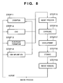
- Fig. 8 shows the detailed flow of the above-mentioned wafer process.
- step 11 oxidation
- step 12 CVD
- step 13 electrode formation
- step 14 ion implantation
- step 14 ion implantation
- step 15 resist processing
- step 16 exposure
- step 18 etching
- step 18 etching
- step 19 resist removal
- Embodiments of the present invention may help to increase, e.g., the productivity of devices.
Landscapes
- Physics & Mathematics (AREA)
- General Physics & Mathematics (AREA)
- Exposure And Positioning Against Photoresist Photosensitive Materials (AREA)
- Exposure Of Semiconductors, Excluding Electron Or Ion Beam Exposure (AREA)
Applications Claiming Priority (2)
| Application Number | Priority Date | Filing Date | Title |
|---|---|---|---|
| JP2002172829 | 2002-06-13 | ||
| JP2002172829A JP2004022655A (ja) | 2002-06-13 | 2002-06-13 | 半導体露光装置及びその制御方法、並びに半導体デバイスの製造方法 |
Publications (2)
| Publication Number | Publication Date |
|---|---|
| EP1372041A2 true EP1372041A2 (fr) | 2003-12-17 |
| EP1372041A3 EP1372041A3 (fr) | 2006-01-11 |
Family
ID=29561798
Family Applications (1)
| Application Number | Title | Priority Date | Filing Date |
|---|---|---|---|
| EP03253658A Withdrawn EP1372041A3 (fr) | 2002-06-13 | 2003-06-10 | Réglage d'un appareil pour l'exposition d'un dispositif semiconducteur |
Country Status (3)
| Country | Link |
|---|---|
| US (1) | US6876438B2 (fr) |
| EP (1) | EP1372041A3 (fr) |
| JP (1) | JP2004022655A (fr) |
Cited By (1)
| Publication number | Priority date | Publication date | Assignee | Title |
|---|---|---|---|---|
| KR20210031602A (ko) * | 2019-09-12 | 2021-03-22 | 주식회사 히타치하이테크 | 패턴 높이 정보 보정 시스템 및 패턴 높이 정보의 보정 방법 |
Families Citing this family (13)
| Publication number | Priority date | Publication date | Assignee | Title |
|---|---|---|---|---|
| US7170075B2 (en) * | 2002-07-18 | 2007-01-30 | Rudolph Technologies, Inc. | Inspection tool with a 3D point sensor to develop a focus map |
| JP4028814B2 (ja) * | 2003-04-21 | 2007-12-26 | 川崎重工業株式会社 | マッピング装置 |
| US7196300B2 (en) * | 2003-07-18 | 2007-03-27 | Rudolph Technologies, Inc. | Dynamic focusing method and apparatus |
| JP2005191393A (ja) * | 2003-12-26 | 2005-07-14 | Canon Inc | 露光方法及び装置 |
| JP2006165371A (ja) * | 2004-12-09 | 2006-06-22 | Canon Inc | 転写装置およびデバイス製造方法 |
| JP2009200105A (ja) * | 2008-02-19 | 2009-09-03 | Canon Inc | 露光装置 |
| WO2012081234A1 (fr) * | 2010-12-14 | 2012-06-21 | 株式会社ニコン | Procédé d'exposition, appareil d'exposition et procédé de fabrication d'un dispositif |
| JP6071263B2 (ja) * | 2012-06-22 | 2017-02-01 | キヤノン株式会社 | 露光装置、露光システム、それらを用いたデバイスの製造方法 |
| JP2014041211A (ja) * | 2012-08-21 | 2014-03-06 | Canon Inc | 露光システム、露光装置、それを用いたデバイスの製造方法 |
| EP2752870A1 (fr) * | 2013-01-04 | 2014-07-09 | Süss Microtec Lithography GmbH | Mandrin, en particulier pour utilisation dans un aligneur de masques |
| JP6381180B2 (ja) * | 2013-06-21 | 2018-08-29 | キヤノン株式会社 | 露光装置、情報管理装置、露光システムおよびデバイス製造方法 |
| KR102253902B1 (ko) | 2016-11-02 | 2021-05-20 | 에이에스엠엘 네델란즈 비.브이. | 높이 센서, 리소그래피 장치 및 디바이스 제조 방법 |
| CN117930602B (zh) * | 2024-03-21 | 2024-07-02 | 上海图双精密装备有限公司 | 掩膜对准系统和方法、以及光刻机 |
Family Cites Families (14)
| Publication number | Priority date | Publication date | Assignee | Title |
|---|---|---|---|---|
| JP2770960B2 (ja) | 1988-10-06 | 1998-07-02 | キヤノン株式会社 | Sor−x線露光装置 |
| JPH05152186A (ja) * | 1991-05-01 | 1993-06-18 | Canon Inc | 測定装置及び露光装置及び露光装置の位置決め方法 |
| US5777722A (en) * | 1994-04-28 | 1998-07-07 | Nikon Corporation | Scanning exposure apparatus and method |
| JP3555230B2 (ja) * | 1994-05-18 | 2004-08-18 | 株式会社ニコン | 投影露光装置 |
| JP3634068B2 (ja) * | 1995-07-13 | 2005-03-30 | 株式会社ニコン | 露光方法及び装置 |
| JP3376179B2 (ja) * | 1995-08-03 | 2003-02-10 | キヤノン株式会社 | 面位置検出方法 |
| JP3377165B2 (ja) | 1997-05-19 | 2003-02-17 | キヤノン株式会社 | 半導体露光装置 |
| JP4208277B2 (ja) * | 1997-11-26 | 2009-01-14 | キヤノン株式会社 | 露光方法及び露光装置 |
| JP4095186B2 (ja) * | 1998-11-20 | 2008-06-04 | キヤノン株式会社 | 露光方法 |
| JP2000228355A (ja) | 1998-12-04 | 2000-08-15 | Canon Inc | 半導体露光装置およびデバイス製造方法 |
| EP1037117A3 (fr) * | 1999-03-08 | 2003-11-12 | ASML Netherlands B.V. | Nivellement hors axe dans un appareil de projection lithographique |
| JP4585649B2 (ja) * | 2000-05-19 | 2010-11-24 | キヤノン株式会社 | 露光装置およびデバイス製造方法 |
| KR100471018B1 (ko) * | 2000-11-28 | 2005-03-08 | 스미도모쥬기가이고교 가부시키가이샤 | 두 개의 대상물 간의 갭 조절장치 및 조절방법 |
| US6836316B2 (en) | 2001-07-26 | 2004-12-28 | Canon Kabushiki Kaisha | Substrate holding apparatus and exposure apparatus using the same |
-
2002
- 2002-06-13 JP JP2002172829A patent/JP2004022655A/ja not_active Withdrawn
-
2003
- 2003-06-05 US US10/454,577 patent/US6876438B2/en not_active Expired - Fee Related
- 2003-06-10 EP EP03253658A patent/EP1372041A3/fr not_active Withdrawn
Cited By (1)
| Publication number | Priority date | Publication date | Assignee | Title |
|---|---|---|---|---|
| KR20210031602A (ko) * | 2019-09-12 | 2021-03-22 | 주식회사 히타치하이테크 | 패턴 높이 정보 보정 시스템 및 패턴 높이 정보의 보정 방법 |
Also Published As
| Publication number | Publication date |
|---|---|
| JP2004022655A (ja) | 2004-01-22 |
| US6876438B2 (en) | 2005-04-05 |
| EP1372041A3 (fr) | 2006-01-11 |
| US20030230730A1 (en) | 2003-12-18 |
Similar Documents
| Publication | Publication Date | Title |
|---|---|---|
| US5742067A (en) | Exposure method and apparatus therefor | |
| JP4029183B2 (ja) | 投影露光装置及び投影露光方法 | |
| US7701553B2 (en) | Surface level detection method, exposure apparatus, and device manufacturing method | |
| US5249016A (en) | Semiconductor device manufacturing system | |
| US7001674B2 (en) | Exposure method, exposure apparatus, and method of production of device | |
| US6236447B1 (en) | Exposure method and apparatus, and semiconductor device manufactured using the method | |
| JP4434372B2 (ja) | 投影露光装置およびデバイス製造方法 | |
| US5403754A (en) | Lithography method for direct alignment of integrated circuits multiple layers | |
| US20020037460A1 (en) | Stage unit, measurement unit and measurement method, and exposure apparatus and exposure method | |
| US6876438B2 (en) | Semiconductor exposure apparatus, control method therefor, and semiconductor device manufacturing method | |
| US6501532B2 (en) | Exposure apparatus and method of controlling the same | |
| JP3962648B2 (ja) | ディストーション計測方法と露光装置 | |
| US7248335B2 (en) | Exposure apparatus, device manufacturing method, stage apparatus, and alignment method | |
| US20030020889A1 (en) | Stage unit, measurement unit and measurement method, and exposure apparatus and exposure method | |
| JP2003254710A (ja) | 面位置検出装置及び方法並びに露光装置と該露光装置を用いたデバイスの製造方法 | |
| US6876435B2 (en) | Exposure method, plane alignment method, exposure apparatus, and device manufacturing method | |
| EP0702272B1 (fr) | Appareil d'exposition et méthode d'exposition | |
| KR20080096433A (ko) | 노광 장치 및 디바이스 제조 방법 | |
| JP3335126B2 (ja) | 面位置検出装置及びそれを用いた走査型投影露光装置 | |
| US7852458B2 (en) | Exposure apparatus | |
| JP5084432B2 (ja) | 露光方法、露光装置およびデバイス製造方法 | |
| JP2002231616A (ja) | 位置計測装置及び方法、露光装置及び方法、並びにデバイス製造方法 | |
| JP2000012455A (ja) | 荷電粒子線転写露光装置及び荷電粒子線転写露光装置におけるマスクと感応基板の位置合わせ方法 | |
| US6243158B1 (en) | Projection exposure apparatus and method | |
| JP2006344739A (ja) | 位置計測装置及びその方法 |
Legal Events
| Date | Code | Title | Description |
|---|---|---|---|
| PUAI | Public reference made under article 153(3) epc to a published international application that has entered the european phase |
Free format text: ORIGINAL CODE: 0009012 |
|
| AK | Designated contracting states |
Kind code of ref document: A2 Designated state(s): AT BE BG CH CY CZ DE DK EE ES FI FR GB GR HU IE IT LI LU MC NL PT RO SE SI SK TR |
|
| AX | Request for extension of the european patent |
Extension state: AL LT LV MK |
|
| PUAL | Search report despatched |
Free format text: ORIGINAL CODE: 0009013 |
|
| AK | Designated contracting states |
Kind code of ref document: A3 Designated state(s): AT BE BG CH CY CZ DE DK EE ES FI FR GB GR HU IE IT LI LU MC NL PT RO SE SI SK TR |
|
| AX | Request for extension of the european patent |
Extension state: AL LT LV MK |
|
| 17P | Request for examination filed |
Effective date: 20060711 |
|
| AKX | Designation fees paid |
Designated state(s): DE FR GB IT NL |
|
| STAA | Information on the status of an ep patent application or granted ep patent |
Free format text: STATUS: THE APPLICATION HAS BEEN WITHDRAWN |
|
| 18W | Application withdrawn |
Effective date: 20070227 |