EP1374246B1 - Systemes et procedes de memoire moleculaire - Google Patents
Systemes et procedes de memoire moleculaire Download PDFInfo
- Publication number
- EP1374246B1 EP1374246B1 EP02709873A EP02709873A EP1374246B1 EP 1374246 B1 EP1374246 B1 EP 1374246B1 EP 02709873 A EP02709873 A EP 02709873A EP 02709873 A EP02709873 A EP 02709873A EP 1374246 B1 EP1374246 B1 EP 1374246B1
- Authority
- EP
- European Patent Office
- Prior art keywords
- molecular
- electrode structure
- memory system
- molecular memory
- recording layer
- Prior art date
- Legal status (The legal status is an assumption and is not a legal conclusion. Google has not performed a legal analysis and makes no representation as to the accuracy of the status listed.)
- Expired - Lifetime
Links
Images


Classifications
-
- H—ELECTRICITY
- H10—SEMICONDUCTOR DEVICES; ELECTRIC SOLID-STATE DEVICES NOT OTHERWISE PROVIDED FOR
- H10D—INORGANIC ELECTRIC SEMICONDUCTOR DEVICES
- H10D84/00—Integrated devices formed in or on semiconductor substrates that comprise only semiconducting layers, e.g. on Si wafers or on GaAs-on-Si wafers
-
- B—PERFORMING OPERATIONS; TRANSPORTING
- B82—NANOTECHNOLOGY
- B82Y—SPECIFIC USES OR APPLICATIONS OF NANOSTRUCTURES; MEASUREMENT OR ANALYSIS OF NANOSTRUCTURES; MANUFACTURE OR TREATMENT OF NANOSTRUCTURES
- B82Y10/00—Nanotechnology for information processing, storage or transmission, e.g. quantum computing or single electron logic
-
- G—PHYSICS
- G11—INFORMATION STORAGE
- G11B—INFORMATION STORAGE BASED ON RELATIVE MOVEMENT BETWEEN RECORD CARRIER AND TRANSDUCER
- G11B9/00—Recording or reproducing using a method not covered by one of the main groups G11B3/00 - G11B7/00; Record carriers therefor
- G11B9/12—Recording or reproducing using a method not covered by one of the main groups G11B3/00 - G11B7/00; Record carriers therefor using near-field interactions; Record carriers therefor
- G11B9/14—Recording or reproducing using a method not covered by one of the main groups G11B3/00 - G11B7/00; Record carriers therefor using near-field interactions; Record carriers therefor using microscopic probe means, i.e. recording or reproducing by means directly associated with the tip of a microscopic electrical probe as used in Scanning Tunneling Microscopy [STM] or Atomic Force Microscopy [AFM] for inducing physical or electrical perturbations in a recording medium; Record carriers or media specially adapted for such transducing of information
- G11B9/1409—Heads
-
- G—PHYSICS
- G11—INFORMATION STORAGE
- G11B—INFORMATION STORAGE BASED ON RELATIVE MOVEMENT BETWEEN RECORD CARRIER AND TRANSDUCER
- G11B9/00—Recording or reproducing using a method not covered by one of the main groups G11B3/00 - G11B7/00; Record carriers therefor
- G11B9/12—Recording or reproducing using a method not covered by one of the main groups G11B3/00 - G11B7/00; Record carriers therefor using near-field interactions; Record carriers therefor
- G11B9/14—Recording or reproducing using a method not covered by one of the main groups G11B3/00 - G11B7/00; Record carriers therefor using near-field interactions; Record carriers therefor using microscopic probe means, i.e. recording or reproducing by means directly associated with the tip of a microscopic electrical probe as used in Scanning Tunneling Microscopy [STM] or Atomic Force Microscopy [AFM] for inducing physical or electrical perturbations in a recording medium; Record carriers or media specially adapted for such transducing of information
- G11B9/1418—Disposition or mounting of heads or record carriers
- G11B9/1427—Disposition or mounting of heads or record carriers with provision for moving the heads or record carriers relatively to each other or for access to indexed parts without effectively imparting a relative movement
- G11B9/1436—Disposition or mounting of heads or record carriers with provision for moving the heads or record carriers relatively to each other or for access to indexed parts without effectively imparting a relative movement with provision for moving the heads or record carriers relatively to each other
- G11B9/1454—Positioning the head or record carrier into or out of operative position or across information tracks; Alignment of the head relative to the surface of the record carrier
-
- G—PHYSICS
- G11—INFORMATION STORAGE
- G11B—INFORMATION STORAGE BASED ON RELATIVE MOVEMENT BETWEEN RECORD CARRIER AND TRANSDUCER
- G11B9/00—Recording or reproducing using a method not covered by one of the main groups G11B3/00 - G11B7/00; Record carriers therefor
- G11B9/12—Recording or reproducing using a method not covered by one of the main groups G11B3/00 - G11B7/00; Record carriers therefor using near-field interactions; Record carriers therefor
- G11B9/14—Recording or reproducing using a method not covered by one of the main groups G11B3/00 - G11B7/00; Record carriers therefor using near-field interactions; Record carriers therefor using microscopic probe means, i.e. recording or reproducing by means directly associated with the tip of a microscopic electrical probe as used in Scanning Tunneling Microscopy [STM] or Atomic Force Microscopy [AFM] for inducing physical or electrical perturbations in a recording medium; Record carriers or media specially adapted for such transducing of information
- G11B9/1463—Record carriers for recording or reproduction involving the use of microscopic probe means
- G11B9/1472—Record carriers for recording or reproduction involving the use of microscopic probe means characterised by the form
-
- G—PHYSICS
- G11—INFORMATION STORAGE
- G11B—INFORMATION STORAGE BASED ON RELATIVE MOVEMENT BETWEEN RECORD CARRIER AND TRANSDUCER
- G11B9/00—Recording or reproducing using a method not covered by one of the main groups G11B3/00 - G11B7/00; Record carriers therefor
- G11B9/12—Recording or reproducing using a method not covered by one of the main groups G11B3/00 - G11B7/00; Record carriers therefor using near-field interactions; Record carriers therefor
- G11B9/14—Recording or reproducing using a method not covered by one of the main groups G11B3/00 - G11B7/00; Record carriers therefor using near-field interactions; Record carriers therefor using microscopic probe means, i.e. recording or reproducing by means directly associated with the tip of a microscopic electrical probe as used in Scanning Tunneling Microscopy [STM] or Atomic Force Microscopy [AFM] for inducing physical or electrical perturbations in a recording medium; Record carriers or media specially adapted for such transducing of information
- G11B9/1463—Record carriers for recording or reproduction involving the use of microscopic probe means
- G11B9/149—Record carriers for recording or reproduction involving the use of microscopic probe means characterised by the memorising material or structure
-
- Y—GENERAL TAGGING OF NEW TECHNOLOGICAL DEVELOPMENTS; GENERAL TAGGING OF CROSS-SECTIONAL TECHNOLOGIES SPANNING OVER SEVERAL SECTIONS OF THE IPC; TECHNICAL SUBJECTS COVERED BY FORMER USPC CROSS-REFERENCE ART COLLECTIONS [XRACs] AND DIGESTS
- Y10—TECHNICAL SUBJECTS COVERED BY FORMER USPC
- Y10S—TECHNICAL SUBJECTS COVERED BY FORMER USPC CROSS-REFERENCE ART COLLECTIONS [XRACs] AND DIGESTS
- Y10S977/00—Nanotechnology
- Y10S977/70—Nanostructure
- Y10S977/734—Fullerenes, i.e. graphene-based structures, such as nanohorns, nanococoons, nanoscrolls or fullerene-like structures, e.g. WS2 or MoS2 chalcogenide nanotubes, planar C3N4, etc.
- Y10S977/742—Carbon nanotubes, CNTs
-
- Y—GENERAL TAGGING OF NEW TECHNOLOGICAL DEVELOPMENTS; GENERAL TAGGING OF CROSS-SECTIONAL TECHNOLOGIES SPANNING OVER SEVERAL SECTIONS OF THE IPC; TECHNICAL SUBJECTS COVERED BY FORMER USPC CROSS-REFERENCE ART COLLECTIONS [XRACs] AND DIGESTS
- Y10—TECHNICAL SUBJECTS COVERED BY FORMER USPC
- Y10S—TECHNICAL SUBJECTS COVERED BY FORMER USPC CROSS-REFERENCE ART COLLECTIONS [XRACs] AND DIGESTS
- Y10S977/00—Nanotechnology
- Y10S977/84—Manufacture, treatment, or detection of nanostructure
- Y10S977/849—Manufacture, treatment, or detection of nanostructure with scanning probe
- Y10S977/86—Scanning probe structure
- Y10S977/874—Probe tip array
-
- Y—GENERAL TAGGING OF NEW TECHNOLOGICAL DEVELOPMENTS; GENERAL TAGGING OF CROSS-SECTIONAL TECHNOLOGIES SPANNING OVER SEVERAL SECTIONS OF THE IPC; TECHNICAL SUBJECTS COVERED BY FORMER USPC CROSS-REFERENCE ART COLLECTIONS [XRACs] AND DIGESTS
- Y10—TECHNICAL SUBJECTS COVERED BY FORMER USPC
- Y10S—TECHNICAL SUBJECTS COVERED BY FORMER USPC CROSS-REFERENCE ART COLLECTIONS [XRACs] AND DIGESTS
- Y10S977/00—Nanotechnology
- Y10S977/84—Manufacture, treatment, or detection of nanostructure
- Y10S977/849—Manufacture, treatment, or detection of nanostructure with scanning probe
- Y10S977/86—Scanning probe structure
- Y10S977/875—Scanning probe structure with tip detail
-
- Y—GENERAL TAGGING OF NEW TECHNOLOGICAL DEVELOPMENTS; GENERAL TAGGING OF CROSS-SECTIONAL TECHNOLOGIES SPANNING OVER SEVERAL SECTIONS OF THE IPC; TECHNICAL SUBJECTS COVERED BY FORMER USPC CROSS-REFERENCE ART COLLECTIONS [XRACs] AND DIGESTS
- Y10—TECHNICAL SUBJECTS COVERED BY FORMER USPC
- Y10S—TECHNICAL SUBJECTS COVERED BY FORMER USPC CROSS-REFERENCE ART COLLECTIONS [XRACs] AND DIGESTS
- Y10S977/00—Nanotechnology
- Y10S977/902—Specified use of nanostructure
- Y10S977/932—Specified use of nanostructure for electronic or optoelectronic application
- Y10S977/943—Information storage or retrieval using nanostructure
- Y10S977/947—Information storage or retrieval using nanostructure with scanning probe instrument
Definitions
- This invention relates to molecular memory systems and methods.
- a molecular layer e.g., a Langmuir-Blodgett film
- a pair of electrically conducting layers e.g., a pair of metal layers, a metal layer and a doped semiconductor layer, or a pair of doped semiconductor layers.
- the molecular layer serves as a thin insulating film that may be used in a metal-insulator-metal (MIM) structure, which may be configured as a tunnel junction device or a switching device, or a metal-insulator-semiconductor (MIS) structure, which may be configured as a logic and memory device.
- MIM metal-insulator-metal
- MIS metal-insulator-semiconductor
- U.S. Patent No. 6,128,214 describes another molecular memory device structure that is configured as a molecular electrode crossbar memory (MWCM) system formed from a two-dimensional array of nanometer-scale devices.
- MWCM molecular electrode crossbar memory
- Each MWCM device is formed at the crossing point (or junction) of a pair of crossed electrodes where at least one molecular connector species operates as a bi-stable molecular switch between the pair of crossed electrodes.
- the resulting device structure may be configured as a resistor, a diode or an asymmetric non-linear resistor.
- the state of each MWCM device may be altered by applying a relatively high state-changing voltage and may be sensed with a non-state-changing (or non-destructive) voltage.
- U.S. Patent No. 5,812,516 describes a molecular memory system in which a scanning tunneling microscope probe electrode (or an atomic force microscope probe electrode) is scanned directly above a molecular recording layer and is used to emit electrical signals for writing information to and reading information from localized areas of the molecular recording medium.
- the distance between the probe electrode and the recording medium is maintained constant (e.g., on the order of 1 nm) based upon a detected displacement of the probe electrode caused by an inter-atomic force acting between the probe electrode and the recording medium. In this way, damage that might be caused by contact between the probe electrode and the recording medium may be avoided.
- US-A-3, 833, 894 describes an organic memory device having a substrate, on one surface of which a conductor pattern is provided. On the conductor pattern, an organic material is arranged, on which, in turn, a second conductor pattern is provided. On top of the organic material and on top of the second conductor pattern, a protective layer covering both the organic material and the upper conductor pattern is arranged.
- the invention features a novel molecular memory system that includes a protective layer that is disposed over a molecular recording layer to enable a scanning probe to write information to and read information from a molecular memory element by direct electrical contact without substantial risk of damage to either the scanning probe or the molecular recording medium.
- the invention avoids the high emission currents, which may damage the probe electrode or the recording media, or both, and avoids other difficulties often associated molecular memory systems with non-contacting probe electrodes.
- the invention features a molecular memory system that includes a first electrode structure, a second electrode structure, and a recording medium having a molecular recording layer disposed between the first electrode structure and the second electrode structure.
- the second electrode structure has a substantially planar protective surface exposed for contact with a probe tip and comprises an array of spaced-apart electrodes separated by electrically insulating material.
- Embodiments in accordance with this aspect of the invention may include one or more of the following features.
- the molecular recording layer preferably comprises a switchable molecular species (e.g., a rotaxane molecular species).
- the molecular recording layer preferably has a memory property selectively holding first and second memory states with different current-voltage characteristics and preferably exhibits transition between the first and second memory states upon application of a state-changing voltage across the recording layer.
- the first electrode structure preferably comprises metal layer disposed over a substrate.
- the second electrode structure preferably comprises an array of spaced-apart metal electrodes separated by a metal oxide (e.g., aluminum electrodes separated by aluminum oxide).
- the molecular memory system includes a probe tip that is configured to contact the exposed substantially planar protective surface of the second electrode structure.
- the probe tip preferably comprises a carbon nanotube.
- a scanning assembly may include an array of probe tips, each of which is configured to contact the exposed substantially planar protective surface of the second electrode structure.
- An actuator may be coupled to the array of probe tips and may be configured to adjust the position of the probe tips to maintain contact between each probe tip and the exposed substantially planar surface of the second electrode structure.
- the scanning assembly preferably is configured to scan the probe tip array across the exposed substantially planar protective surface of the second electrode structure.
- a read/write controller preferably is configured to control the application of voltage signals through the scanning assembly probe tips and between the first electrode structure and the electrodes of the second electrode structure.
- the read/write controller preferably is configured to control application of a sensing voltage for determining a local memory state of the molecular recording layer and to control the application of a state-changing voltage for changing a local memory state of the molecular recording layer.
- a lubricant is disposed over the exposed substantially planar protective surface of the second electrode structure.
- the invention features a method of making the above-described molecular memory system.
- a probe array is contacted against the exposed substantially planar protective surface of the second electrode structure of the above-described molecular memory system, and the contacting probe tip array is scanned across the exposed substantially planar protective surface of the second electrode structure.
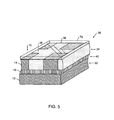
- a molecular memory device (or molecular memory element) 10 includes two electrically conducting electrodes 12, 14 and a layer 16 of switchable molecules or molecular compounds that is sandwiched between electrodes 12, 14.
- the particular molecule or molecules 18 that are located at the junction of electrodes 12, 14 act as switch molecules and correspond to the active portion of molecular memory device 10.
- the state of molecular memory device 10 may be changed by applying a relatively high state-changing voltage across electrodes 12, 14. The magnitude of the state-changing voltage is sufficient to oxidize or reduce switch molecules 18.
- Switch molecules 18 may include a redox pair of molecular species that cooperate to balance charge such that when one of the molecular species is oxidized (or reduced), the other molecular species is reduced (or oxidized).
- one molecular species may be reduced and the associated molecular species (the other half of the redox pair) may be oxidized.
- one molecular species may be reduced and one of the electrodes 12, 14 may be oxidized.
- one molecular species may be oxidized and one of the electrodes 12, 14 may be reduced.
- one electrode may be oxidized and an oxide associated with the other electrode may be reduced.
- oxidation or reduction affects the tunneling distance or the tunneling barrier height between the two electrodes, thereby exponentially altering the rate of charge transport across the electrode junction.
- This electronic functionality serves as the basis for operating molecular memory device 10 as an electrical switch.
- Electrodes 12, 14 each may be formed from an electrically conducting metal or a doped semiconductor material. Electrodes 12, 14 may be deposited onto a substrate 20 by a conventional thin film deposition process, including a physical film deposition process (e.g., magnetron sputtering or electron beam deposition) or a chemical film deposition process (e.g., chemical vapor deposition).
- a physical film deposition process e.g., magnetron sputtering or electron beam deposition
- a chemical film deposition process e.g., chemical vapor deposition
- Molecular layer 16 may be formed from a variety of different switchable molecular species. Other molecular species (e.g., the molecular recording medium compounds described in U.S. Patent No. 5,812,516) also may be used. In some embodiments, the selected molecular species may be dissolved in a solvent (e.g., tetrahydrofuran), prepared as a Langmuir monolayer, and transferred as a Langmuir-Blodgett single molecular monolayer film 16 over bottom electrode 12. In other embodiments, a suitable molecular species may be deposited directly onto substrate 20.
- a solvent e.g., tetrahydrofuran
- Top electrode 14 is surrounded by insulating material 36, which may be formed from any suitable electrically insulating material, including a metal or semiconductor oxide.
- top electrode 14 may be formed by converting regions of a top layer from one electrical conductivity type to another.
- the top layer is formed from an electrical conductor (e.g., aluminum or titanium) and insulating regions 36 are converted to an electrical insulator by a conventional oxidation process.
- the top layer is formed from an electrical insulator (e.g., an electrical antifuse structure), in which case a region corresponding to top electrode 14 is converted to an electrical conductor.
- Substrate 20 may be formed from an insulating material, for example, an oxide layer formed on a semiconductor substrate (e.g., a silicon dioxide (Si0 2 ) layer that is formed on a silicon substrate) or sapphire.
- a semiconductor substrate e.g., a silicon dioxide (Si0 2 ) layer that is formed on a silicon substrate
- sapphire e.g., a silicon dioxide (Si0 2 ) layer that is formed on a silicon substrate
- molecular memory device 10 may exhibit any one of a variety of different electrical switching functions that may be used to controllably connect or disconnect bottom electrode 12 and top electrode 14.
- the molecular memory device may be singly configurable or reconfigurable. In singly configurable embodiments, the initial state of molecular memory device 10 may be open or closed. In reconfigurable embodiments, the switching device may be opened and closed multiple times by cycling the polarity and the magnitude of the applied voltage beyond appropriate threshold values that are selected to reversibly oxidize and reduce the active material or molecules 18.
- the type of electrical connection formed between bottom electrode 12 and top electrode 14 depends upon the materials from which electrodes 12, 14 and molecular layer 16 are formed. Table 1 identifies the various types of electrical switching functions that may be obtained from different device material combinations. TABLE 1 Device Type Electrode Materials Metal-Metal (same) Metal-Metal (different) Metal-Semiconductor Semiconductor-Semiconductor (pn junction) Semiconductor-Semiconductor (heterojunction) Resistor X X X Tunneling Resistor X X X Resonant Tunneling Resistor X X X Diode X X X X X Tunneling Diode X X X X Resonant Tunneling Diode X X X X Battery X X X X
- a molecular memory 30 may be formed from an array of memory elements each having the structure of molecular memory device 10.
- molecular memory system 30 includes a first electrode structure 32 that corresponds to electrode 12, which serves as a common electrode for each of the memory elements.
- Molecular memory system 30 also includes a second electrode structure 34 that includes an array of spaced-apart electrodes 14 separated by electrically insulating material 36 and has a substantially planar protective surface 38 that is exposed for contact with a scanning probe tip.
- a recording medium 40 which corresponds to molecular layer 16, is disposed between first electrode structure 32 and second electrode structure 34.
- information may be written into and read from molecular memory 30 with one or an array of probe tips 50 that are supported by a scanning head 52.
- a read/write controller 54 controls the application of voltage signals through probe tips 50 and between first electrode structure 32 and the electrodes 14 of second electrode structure 34.
- scanning head 52 is mounted on a scanning assembly 59 that is configured to precisely move scanning head 52 over the exposed substantially planar protective surface 38 of second electrode structure 34.
- scanning head 52 may be moved vertically by a z-axis scan actuator 60 and may be moved horizontally by an x-y axis scan actuator 62.
- Z-axis scan actuator 60 and x-y axis scan actuator 62 are carried by a support arm 64.
- a positioning controller 66 controls the vertical and horizontal positions of probe tips 50 over surface 38. In operation, positioning controller 66 may lower probe tips 50 vertically into contact with surface 38. Subsequently, positioning controller 66 may scan the contacting probe tips 50 horizontally across surface 38. After one or more probe tips 50 are positioned over a respective number of electrodes 14, read/write controller 54 may write information into the corresponding memory elements by applying across the memory elements a relatively high state-changing voltage that is selected to change the local memory states of the memory elements. Alternatively, read/write controller 54 may read information stored in the corresponding memory elements by applying across the memory elements a relatively low sensing voltage that is selected to provide information about the electrical current conducting properties of the memory elements without changing their memory states.
- Scanning assembly 59 may be implemented as a conventional scanning tunneling microscope (STM) scanning assembly, in which the positions of probe tips 50 are controlled based upon tunneling current information.
- scanning assembly 59 may be implemented as an atomic force microscope (AFM) scanning assembly, in which the positions of probe tips 50 are controlled based upon a force (e.g., an atomic force, an electrostatic force, or a magnetic force) that is generated between probe tips 50 and the exposed substantially planar protective surface 38 of second electrode structure 34.
- Z-axis scan actuator 60 and x-y axis scan actuator 62 may be implemented as planar electrostatic actuators (see, e.g., U.S. Patent Nos. 6,136,208 and 5,801,472, which are incorporated herein by reference).
- scanning head 52 may support a regular array of probe tips 50 with a probe tip spacing that preferably corresponds to 10-10 4 times the spacing between memory elements 10 of molecular memory 30.
- Probe tips 50 may be formed from a durable, resilient and electrically conductive material, including a metallic material (e.g., platinum) or non-metallic material (e.g., carbon).
- probe tips 50 are carbon nanotubes.
- the term "nanotube” means a hollow article having a narrow dimension (diameter) of about 1-200 nm and a long dimension (length), where the ratio of the long dimension to the narrow dimension (i.e., the aspect ratio) is at least 5.
- each probe tip 50 may be either a multi-walled nanotube (MWNT) or a single-walled nanotube (SWNT).
- MWNT includes several nanotubes each having a different diameter.
- SWNT includes only one nanotube.
- MWNTs typically are produced either as single MWNTs or as bundles of MWNTs.
- SWNTs typically are produced as ropes of SWNTs, where each strand of the rope is a SWNT.
- the carbon nanotube probe tips 50 may be grown by a conventional carbon nanotube fabrication process (e.g., chemical vapor deposition).
- a planar actuator 80 is positioned at the base of each probe tip 50 and is configured to maintain each probe tip 50 in contact with surface 38.
- the carbon nanotube probe tips 50 may have the same or different lengths.
- planar actuator 80 is configured to adjust the position of each probe tip 50 to accommodate the respective probe tip lengths so as to maintain contact between the probe tips 50 and surface 38.
- a lubricant layer 70 may be disposed over the exposed substantially planar protective surface 38 of second electrode structure 34.
- Lubricant layer 70 may be formed from any suitable electrically non-conducting solid or liquid material that reduces the interaction energy between probe tips 50 and surface 38.
- lubricant 70 may be a graphite layer that is thermally evaporated over surface 38. Other material compositions also may be used. By reducing the interaction energy between the contacting probe tips 50 and surface 38, lubricant layer 70 reduces wear of and the likelihood of damage to probe tips 50 and surface 38 during use.
- molecular memory devices may be implemented in a circuit designed to perform one or more logic (as opposed to memory) functions.
Landscapes
- Engineering & Computer Science (AREA)
- Chemical & Material Sciences (AREA)
- Nanotechnology (AREA)
- Physics & Mathematics (AREA)
- Mathematical Physics (AREA)
- Theoretical Computer Science (AREA)
- Crystallography & Structural Chemistry (AREA)
- Semiconductor Memories (AREA)
Abstract
Claims (18)
- Système de mémoire moléculaire, comprenant :une première structure d'électrode (32) ;un support d'enregistrement (40) ayant une couche d'enregistrement moléculaire (16) placée entre la première structure d'électrode (32) et une seconde structure d'électrode (34) ;caractérisé par la seconde structure d'électrode (34) ayant une surface protectrice sensiblement plane (38) exposée pour être en contact avec une pointe de sonde (50) et comprenant un réseau d'électrodes espacées (14) séparées par un matériau électriquement isolant (36); et dans lequel les électrodes (14) de la seconde structure d'électrode (34) sont entourées par le matériau électriquement isolant (36) de sorte que les surfaces de la seconde structure d'électrode (34) et le matériau électriquement isolant (36) étant opposés au support d'enregistrement (40) forment la surface protectrice plane (38).
- Système de mémoire moléculaire selon la revendication 1, dans lequel la couche d'enregistrement moléculaire (16) comprend une espèce moléculaire commutable.
- Système de mémoire moléculaire selon la revendication 2, dans lequel la couche d'enregistrement moléculaire (16) comprend une espèce moléculaire de rotaxane.
- Système de mémoire moléculaire selon la revendication 1, dans lequel la première structure d'électrode (32) comprend une couche métallique (12) placée sur un substrat (20).
- Système de mémoire moléculaire selon la revendication 1, dans lequel la seconde structure d'électrode (34) comprend un réseau d'électrodes espacées (14) séparées par un oxyde métallique (36).
- Système de mémoire moléculaire selon la revendication 5, dans lequel les électrodes métalliques (14) sont formées à partir d'aluminium et l'oxyde métallique (36) est de l'oxyde d'aluminium.
- Système de mémoire moléculaire selon la revendication 1, comprenant en outre une pointe de sonde (50) configurée pour être en contact avec la surface protectrice sensiblement plane (38) exposée de la seconde structure d'électrode (32).
- Système de mémoire moléculaire selon la revendication 7, dans lequel la pointe de sonde (50) comprend un nanotube de carbone.
- Système de mémoire moléculaire selon la revendication 1, comprenant en outre un ensemble de balayage (52) comprenant une matrice de pointes de sonde (50), chacune configurée pour être en contact avec la surface protectrice sensiblement plane exposée (38) de la seconde structure d'électrode (34).
- Système de mémoire moléculaire selon la revendication 9, comprenant en outre un actionneur (60) couplé à la matrice de pointes de sonde (50) et configuré pour ajuster la position des pointes de sonde (50) afin de maintenir le contact entre chaque pointe de sonde (50) et la surface sensiblement plane exposée (38) de la seconde structure d'électrode (34).
- Système de mémoire moléculaire selon la revendication 9, dans lequel l'ensemble de balayage (59) est configuré pour balayer la matrice de pointes de sonde à travers la surface protectrice sensiblement plane exposée (38) de la seconde structure d'électrode (34).
- Système de mémoire moléculaire selon la revendication 11, comprenant en outre un contrôleur de lecture/écriture (54) configuré pour réguler l'application de signaux de tension à travers les pointes de sonde de l'ensemble de balayage (50) et entre la première structure d'électrode (32) et les électrodes (14) de la seconde structure d'électrode (34)
- Système de mémoire moléculaire selon la revendication 12, dans lequel la couche d'enregistrement moléculaire (16) a une propriété de mémoire maintenant sélectivement des premier et second états de mémoire avec différentes caractéristiques de courant-tension et produit une transition entre les premier et second états de mémoire par application d'une tension de changement d'état au travers de la couche d'enregistrement (16).
- Système de mémoire moléculaire selon la revendication 13, dans lequel le contrôleur d'écriture/lecture (54) est configuré pour réguler l'application d'une tension de détection destinée à déterminer un état de mémoire locale de la couche d'enregistrement moléculaire (16) et pour réguler l'application d'une tension de changement d'état destinée à modifier un état de mémoire locale de la couche d'enregistrement moléculaire (16).
- Système de mémoire moléculaire selon la revendication 1, comprenant en outre un lubrifiant (70) placé sur la surface protectrice sensiblement plane exposée (38) de la seconde structure d'électrode (34).
- Système de mémoire moléculaire, comprenant :la fourniture d'un système de mémoire moléculaire (30) tel que défini selon l'une des revendications 1 à 15 ;la mise en contact d'une matrice de sonde (50) contre la surface protectrice sensiblement plane exposée (38) de la seconde structure d'électrode (34) ; etle balayage de la matrice de pointes de sonde (50) en contact à travers la surface protectrice sensiblement plane exposée (38) de la seconde structure d'électrode (34).
- Procédé de mémoire moléculaire selon la revendication 16, comprenant en outre l'application au travers de la couche d'enregistrement moléculaire (16) d'une tension de détection destinée à déterminer un état de mémoire locale de la couche d'enregistrement moléculaire (16).
- Procédé de mémoire moléculaire selon la revendication 16, comprenant en outre l'application au travers de la couche d'enregistrement moléculaire (16) d'une tension de changement d'état destiné à modifier un état de mémoire locale de la couche d'enregistrement moléculaire (16).
Applications Claiming Priority (3)
| Application Number | Priority Date | Filing Date | Title |
|---|---|---|---|
| US819402 | 2001-03-27 | ||
| US09/819,402 US6542400B2 (en) | 2001-03-27 | 2001-03-27 | Molecular memory systems and methods |
| PCT/US2002/008863 WO2002078005A2 (fr) | 2001-03-27 | 2002-03-21 | Systemes et procedes de memoire moleculaire |
Publications (2)
| Publication Number | Publication Date |
|---|---|
| EP1374246A2 EP1374246A2 (fr) | 2004-01-02 |
| EP1374246B1 true EP1374246B1 (fr) | 2007-05-09 |
Family
ID=25228051
Family Applications (1)
| Application Number | Title | Priority Date | Filing Date |
|---|---|---|---|
| EP02709873A Expired - Lifetime EP1374246B1 (fr) | 2001-03-27 | 2002-03-21 | Systemes et procedes de memoire moleculaire |
Country Status (6)
| Country | Link |
|---|---|
| US (1) | US6542400B2 (fr) |
| EP (1) | EP1374246B1 (fr) |
| JP (1) | JP4171304B2 (fr) |
| KR (1) | KR100867220B1 (fr) |
| DE (1) | DE60220037T2 (fr) |
| WO (1) | WO2002078005A2 (fr) |
Families Citing this family (33)
| Publication number | Priority date | Publication date | Assignee | Title |
|---|---|---|---|---|
| US7260051B1 (en) | 1998-12-18 | 2007-08-21 | Nanochip, Inc. | Molecular memory medium and molecular memory integrated circuit |
| US20020138301A1 (en) * | 2001-03-22 | 2002-09-26 | Thanos Karras | Integration of a portal into an application service provider data archive and/or web based viewer |
| US6995312B2 (en) * | 2001-03-29 | 2006-02-07 | Hewlett-Packard Development Company, L.P. | Bistable molecular switches and associated methods |
| US6928042B2 (en) * | 2001-07-06 | 2005-08-09 | Hewlett-Packard Development Company, L.P. | Data storage device including nanotube electron sources |
| TW506083B (en) * | 2001-11-28 | 2002-10-11 | Ind Tech Res Inst | Method of using nano-tube to increase semiconductor device capacitance |
| EP1341183B1 (fr) * | 2002-02-25 | 2008-12-03 | STMicroelectronics S.r.l. | Mémoire moléculaire optiquement lisible réalisée avec l'aide de nanotubes à carbone et procédé pour la mémorisation d'information dans cette mémoire moléculaire |
| US6985377B2 (en) | 2002-10-15 | 2006-01-10 | Nanochip, Inc. | Phase change media for high density data storage |
| US7233517B2 (en) | 2002-10-15 | 2007-06-19 | Nanochip, Inc. | Atomic probes and media for high density data storage |
| US20040150472A1 (en) * | 2002-10-15 | 2004-08-05 | Rust Thomas F. | Fault tolerant micro-electro mechanical actuators |
| US6982898B2 (en) * | 2002-10-15 | 2006-01-03 | Nanochip, Inc. | Molecular memory integrated circuit utilizing non-vibrating cantilevers |
| ITBO20020759A1 (it) * | 2002-12-04 | 2004-06-05 | Fabio Biscarini | Procedimento per lo stoccaggio di informazione ad |
| US6961299B2 (en) * | 2002-12-05 | 2005-11-01 | Hewlett-Packard Development Company, L.P. | Storage device |
| US7057997B2 (en) * | 2003-04-23 | 2006-06-06 | Hewlett-Packard Development Company, L.P. | Class of electron beam based data storage devices and methods of use thereof |
| AU2003237713A1 (en) * | 2003-05-26 | 2004-12-13 | Nardy Cramm | Information storage basec on carbon nanotubes |
| FR2856184B1 (fr) * | 2003-06-13 | 2008-04-11 | Commissariat Energie Atomique | Dispositif d'enregistrement de donnees comportant des micro-pointes et un support d'enregistrement |
| JP4898436B2 (ja) * | 2003-07-03 | 2012-03-14 | コミサリア ア レネルジー アトミック エ オ ゼネルジー アルテルナティブ | データ記録方法及びこの方法を実施する、変形可能なメモリ支持体を有する装置 |
| EP1580739A1 (fr) * | 2004-03-23 | 2005-09-28 | DSM IP Assets B.V. | Objet comprenant une couche fonctionnelle |
| US7499309B1 (en) * | 2004-04-02 | 2009-03-03 | Spansion Llc | Using organic semiconductor memory in conjunction with a MEMS actuator for an ultra high density memory |
| US7301887B2 (en) * | 2004-04-16 | 2007-11-27 | Nanochip, Inc. | Methods for erasing bit cells in a high density data storage device |
| US7379412B2 (en) | 2004-04-16 | 2008-05-27 | Nanochip, Inc. | Methods for writing and reading highly resolved domains for high density data storage |
| US20050232061A1 (en) | 2004-04-16 | 2005-10-20 | Rust Thomas F | Systems for writing and reading highly resolved domains for high density data storage |
| US7002820B2 (en) * | 2004-06-17 | 2006-02-21 | Hewlett-Packard Development Company, L.P. | Semiconductor storage device |
| FR2876831B1 (fr) * | 2004-10-15 | 2007-02-02 | Commissariat Energie Atomique | Dispositif d'enregistrement de donnees comportant des nanotubes de carbone inclines et procede de fabrication |
| KR100734832B1 (ko) * | 2004-12-15 | 2007-07-03 | 한국전자통신연구원 | 금속 산화막의 전류 스위칭을 이용한 정보 저장 장치 |
| FR2880980B1 (fr) * | 2005-01-17 | 2007-03-16 | Commissariat Energie Atomique | Dispositif d'enregistrement de donnees comportant des micro-pointes dont l'ensemble des extremites libres forme une surface convexe et procede de fabrication |
| US20060238185A1 (en) * | 2005-04-08 | 2006-10-26 | Kozicki Michael N | Probe storage device, system including the device, and methods of forming and using same |
| US20060291364A1 (en) * | 2005-04-25 | 2006-12-28 | Kozicki Michael N | Solid electrolyte probe storage device, system including the device, and methods of forming and using same |
| US7463573B2 (en) | 2005-06-24 | 2008-12-09 | Nanochip, Inc. | Patterned media for a high density data storage device |
| US7367119B2 (en) * | 2005-06-24 | 2008-05-06 | Nanochip, Inc. | Method for forming a reinforced tip for a probe storage device |
| US7309630B2 (en) * | 2005-07-08 | 2007-12-18 | Nanochip, Inc. | Method for forming patterned media for a high density data storage device |
| US7357538B2 (en) * | 2006-01-25 | 2008-04-15 | Cooper Technologies Company | Method and apparatus for providing light |
| FR2901909B1 (fr) * | 2006-05-30 | 2008-10-24 | Commissariat Energie Atomique | Memoire de donnees inscriptible et lisible par micropointes, structuree en caissons, et procede de fabrication |
| JP2008243238A (ja) * | 2007-03-23 | 2008-10-09 | Elpida Memory Inc | 分子電池メモリ装置 |
Family Cites Families (21)
| Publication number | Priority date | Publication date | Assignee | Title |
|---|---|---|---|---|
| US3833894A (en) | 1973-06-20 | 1974-09-03 | Ibm | Organic memory device |
| US4188434A (en) * | 1978-05-15 | 1980-02-12 | Storage Technology Corporation | Lubricant for a magnetic member |
| DE3752099T2 (de) * | 1986-12-24 | 1997-11-13 | Canon Kk | Aufzeichnungsgerät und Wiedergabegerät |
| JP2557964B2 (ja) | 1988-01-22 | 1996-11-27 | インターナシヨナル・ビジネス・マシーンズ・コーポレイーシヨン | データ記憶装置 |
| JP2756254B2 (ja) | 1988-03-25 | 1998-05-25 | キヤノン株式会社 | 記録装置及び再生装置 |
| NL8802335A (nl) | 1988-09-21 | 1990-04-17 | Philips Nv | Werkwijze en inrichting voor het op sub-mikron schaal bewerken van een materiaal-oppervlak. |
| US5264876A (en) * | 1989-08-10 | 1993-11-23 | Canon Kabushiki Kaisha | Recording medium, method for preparing the same, recording and reproducing device, and recording, reproducing and erasing method by use of such recording medium |
| JPH05282706A (ja) * | 1991-08-01 | 1993-10-29 | Canon Inc | 光記録媒体とその製造方法及び光記録媒体用基板 |
| EP0591595A1 (fr) | 1992-10-08 | 1994-04-13 | International Business Machines Corporation | Méthode d'enregistrement/reproduction moléculaire et milieu d'enregistrement |
| JP3053986B2 (ja) | 1993-01-21 | 2000-06-19 | キヤノン株式会社 | 記録再生装置 |
| US5453970A (en) | 1993-07-13 | 1995-09-26 | Rust; Thomas F. | Molecular memory medium and molecular memory disk drive for storing information using a tunnelling probe |
| US5801472A (en) | 1995-08-18 | 1998-09-01 | Hitchi, Ltd. | Micro-fabricated device with integrated electrostatic actuator |
| US6195313B1 (en) | 1997-08-29 | 2001-02-27 | Canon Kabushiki Kaisha | Tracking mechanism and method using probes for information recording/reproducing apparatus |
| US6246652B1 (en) * | 1997-12-05 | 2001-06-12 | Hitachi, Ltd. | Device using sensor for small rotation angle |
| US6159742A (en) | 1998-06-05 | 2000-12-12 | President And Fellows Of Harvard College | Nanometer-scale microscopy probes |
| US5930162A (en) | 1998-09-30 | 1999-07-27 | Motorola, Inc. | Quantum random address memory with polymer mixer and/or memory |
| US6128214A (en) | 1999-03-29 | 2000-10-03 | Hewlett-Packard | Molecular wire crossbar memory |
| US6256767B1 (en) * | 1999-03-29 | 2001-07-03 | Hewlett-Packard Company | Demultiplexer for a molecular wire crossbar network (MWCN DEMUX) |
| TW408417B (en) | 1999-05-03 | 2000-10-11 | Ind Tech Res Inst | Planar-shape thin probe having electrostatic actuator manufactured by using sacrificed layer technology and its manufacturing method |
| US6062931A (en) | 1999-09-01 | 2000-05-16 | Industrial Technology Research Institute | Carbon nanotube emitter with triode structure |
| JP4467116B2 (ja) * | 1999-12-20 | 2010-05-26 | 富士電機デバイステクノロジー株式会社 | 磁気記録媒体 |
-
2001
- 2001-03-27 US US09/819,402 patent/US6542400B2/en not_active Expired - Fee Related
-
2002
- 2002-03-21 KR KR1020037012546A patent/KR100867220B1/ko not_active Expired - Fee Related
- 2002-03-21 JP JP2002575955A patent/JP4171304B2/ja not_active Expired - Fee Related
- 2002-03-21 DE DE60220037T patent/DE60220037T2/de not_active Expired - Lifetime
- 2002-03-21 WO PCT/US2002/008863 patent/WO2002078005A2/fr not_active Ceased
- 2002-03-21 EP EP02709873A patent/EP1374246B1/fr not_active Expired - Lifetime
Also Published As
| Publication number | Publication date |
|---|---|
| JP2004532494A (ja) | 2004-10-21 |
| WO2002078005A3 (fr) | 2002-12-19 |
| KR20030085060A (ko) | 2003-11-01 |
| US20020172072A1 (en) | 2002-11-21 |
| US6542400B2 (en) | 2003-04-01 |
| EP1374246A2 (fr) | 2004-01-02 |
| DE60220037T2 (de) | 2008-02-14 |
| DE60220037D1 (de) | 2007-06-21 |
| KR100867220B1 (ko) | 2008-11-06 |
| JP4171304B2 (ja) | 2008-10-22 |
| WO2002078005A2 (fr) | 2002-10-03 |
Similar Documents
| Publication | Publication Date | Title |
|---|---|---|
| EP1374246B1 (fr) | Systemes et procedes de memoire moleculaire | |
| US7298016B2 (en) | Electromechanical memory array using nanotube ribbons and method for making same | |
| US6574130B2 (en) | Hybrid circuit having nanotube electromechanical memory | |
| US6643165B2 (en) | Electromechanical memory having cell selection circuitry constructed with nanotube technology | |
| EP2286929B1 (fr) | Procédé de fabrication de rubans conducteurs à nanotubes | |
| US20160232972A1 (en) | Methods of forming nanotube films and articles | |
| US20050281084A1 (en) | Methods of making electromechanical three-trace junction devices | |
| EP0576263B1 (fr) | Procédé pour fabriquer des nano-structures et nano-structure fabriquée selon ce procédé | |
| JPH04321954A (ja) | カンチレバー型プローブ、及びこれを用いた走査型トンネル顕微鏡、情報処理装置 | |
| US7002820B2 (en) | Semiconductor storage device |
Legal Events
| Date | Code | Title | Description |
|---|---|---|---|
| PUAI | Public reference made under article 153(3) epc to a published international application that has entered the european phase |
Free format text: ORIGINAL CODE: 0009012 |
|
| 17P | Request for examination filed |
Effective date: 20030909 |
|
| AK | Designated contracting states |
Kind code of ref document: A2 Designated state(s): AT BE CH CY DE DK ES FI FR GB GR IE IT LI LU MC NL PT SE TR |
|
| 17Q | First examination report despatched |
Effective date: 20040121 |
|
| RIN1 | Information on inventor provided before grant (corrected) |
Inventor name: CHEN, YONG Inventor name: WALMSLEY, ROBERT G, |
|
| RBV | Designated contracting states (corrected) |
Designated state(s): DE |
|
| GRAP | Despatch of communication of intention to grant a patent |
Free format text: ORIGINAL CODE: EPIDOSNIGR1 |
|
| RIC1 | Information provided on ipc code assigned before grant |
Ipc: G11C 13/04 20060101AFI20060913BHEP |
|
| GRAS | Grant fee paid |
Free format text: ORIGINAL CODE: EPIDOSNIGR3 |
|
| GRAA | (expected) grant |
Free format text: ORIGINAL CODE: 0009210 |
|
| AK | Designated contracting states |
Kind code of ref document: B1 Designated state(s): DE |
|
| REF | Corresponds to: |
Ref document number: 60220037 Country of ref document: DE Date of ref document: 20070621 Kind code of ref document: P |
|
| PLBE | No opposition filed within time limit |
Free format text: ORIGINAL CODE: 0009261 |
|
| STAA | Information on the status of an ep patent application or granted ep patent |
Free format text: STATUS: NO OPPOSITION FILED WITHIN TIME LIMIT |
|
| 26N | No opposition filed |
Effective date: 20080212 |
|
| PGFP | Annual fee paid to national office [announced via postgrant information from national office to epo] |
Ref country code: DE Payment date: 20110329 Year of fee payment: 10 |
|
| REG | Reference to a national code |
Ref country code: DE Ref legal event code: R119 Ref document number: 60220037 Country of ref document: DE Effective date: 20121002 |
|
| PG25 | Lapsed in a contracting state [announced via postgrant information from national office to epo] |
Ref country code: DE Free format text: LAPSE BECAUSE OF NON-PAYMENT OF DUE FEES Effective date: 20121002 |