EP1375416A1 - Dispositif microélectromécanique, particulièrement microactionneur pour unité de disque dur, et sa méthode de fabrication - Google Patents
Dispositif microélectromécanique, particulièrement microactionneur pour unité de disque dur, et sa méthode de fabrication Download PDFInfo
- Publication number
- EP1375416A1 EP1375416A1 EP02425407A EP02425407A EP1375416A1 EP 1375416 A1 EP1375416 A1 EP 1375416A1 EP 02425407 A EP02425407 A EP 02425407A EP 02425407 A EP02425407 A EP 02425407A EP 1375416 A1 EP1375416 A1 EP 1375416A1
- Authority
- EP
- European Patent Office
- Prior art keywords
- fixed
- substrate
- mobile
- insulating
- region
- Prior art date
- Legal status (The legal status is an assumption and is not a legal conclusion. Google has not performed a legal analysis and makes no representation as to the accuracy of the status listed.)
- Granted
Links
Images


Classifications
-
- B—PERFORMING OPERATIONS; TRANSPORTING
- B81—MICROSTRUCTURAL TECHNOLOGY
- B81B—MICROSTRUCTURAL DEVICES OR SYSTEMS, e.g. MICROMECHANICAL DEVICES
- B81B3/00—Devices comprising flexible or deformable elements, e.g. comprising elastic tongues or membranes
- B81B3/0018—Structures acting upon the moving or flexible element for transforming energy into mechanical movement or vice versa, i.e. actuators, sensors, generators
- B81B3/0021—Transducers for transforming electrical into mechanical energy or vice versa
-
- H—ELECTRICITY
- H02—GENERATION; CONVERSION OR DISTRIBUTION OF ELECTRIC POWER
- H02N—ELECTRIC MACHINES NOT OTHERWISE PROVIDED FOR
- H02N1/00—Electrostatic generators or motors using a solid moving electrostatic charge carrier
- H02N1/002—Electrostatic motors
- H02N1/006—Electrostatic motors of the gap-closing type
Definitions
- the present invention relates to a micro-electro-mechanical device, in particular a micro-actuator for a hard-disk drive, and a manufacturing process thereof.
- micro-electro-mechanical structures such as micromotors or micro-actuators that can be used for fine position control of reading and writing heads in hard-disk drives.
- a first wafer is designed to house the microstructures, while a second wafer operates as a support for the microstructures and integrates the control circuits of the microstructures.
- EP-A-1 151 962 describes a manufacturing process of the above referred type, which uses integrated silicon plugs for electrically connecting the second wafer to the front of the first wafer, on which the electrical interconnections are formed.
- the rear of the wafer is, instead, fixed to a protective cap, a read/write head or a further wafer.
- the aim of the invention is thus to provide a micro-electro-mechanical device and the manufacturing process thereof which overcomes the disadvantages referred to above.
- micro-electro-mechanical device and the manufacturing process thereof are provided, as defined in claims 1 and 10, respectively.
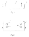
- a first wafer 1 comprising a substrate 4 of semiconductor material, typically heavily doped monocrystalline silicon (for example, an N-type substrate with resistivity of 3 m ⁇ /cm doped with antimony) having a first surface 5, underwent the steps for making trenches, as described in the above-mentioned patent application EP-A-1 151 962.
- the first wafer 1 is masked and etched to form deep trenches 2, here U-shaped, as shown in Figure 2.
- the deep trenches 2 surround biasing portions 3 of monocrystalline silicon and have a depth approximately equal to the final depth of wafer 1, for example, 100 ⁇ m. Further deep trenches 2, of closed form, can be formed also where it is necessary to obtain electrical insulation of part of the first wafer.
- the trenches 2 are filled, either completely or partially, with insulating regions 6, for example of silicon dioxide.
- insulating regions 6, for example of silicon dioxide for example of silicon dioxide.
- a silicon dioxide layer is deposited or grown, and is then removed from the first surface 5 of the first wafer 1, for example by chemical-mechanical polishing (CMP).
- CMP chemical-mechanical polishing
- the first surface 5 of the first wafer is coated with an insulating layer 10, for example thermally grown silicon dioxide, and openings 11 are formed for the contacts.
- the openings are formed, i.a., above the biasing portions 3 of the substrate 4.
- electrical-connection structures are formed and include contacts 12 extending in the openings 11, electrical-connection lines 13, and contact pads 14 (only one whereof can be seen in Figure 5).
- the electrical-connection structures for example of TiNiAu, have a gold finish, to facilitate bonding of the next head.
- a second wafer 18 is bonded to the first wafer 1, to obtain a composite wafer 19.
- the first wafer 1 is bonded on the side comprising the electrical-connection structures, leaving free the rear of the wafer 1.
- Bonding is obtained through bonding regions of suitable material.
- bonding regions 15 of dry resist can be deposited on the front of the wafer and, by masking and etching, be left at scribing lines 16, as shown in Figure 6. Alignment marks are moreover formed on the rear of the second wafer 18, for subsequent identification of the position of the scribing lines.
- the first wafer 1 is thinned out from the rear mechanically, for example by grinding, until the bottom of the trenches 2 is reached, preferably until a thickness of approximately 100 ⁇ m is obtained. In this way a second surface 7 is formed.
- the first wafer 1 is now masked and etched by trench etching starting from the second surface so as to define the desired micromechanical structure, in this case a micro-actuator 20 ( Figure 8).
- second trenches 21 are dug first in the substrate 4 and next in the insulating layer 10 (if it has not been removed previously) so as to separate, from the rest of the substrate 4 (hereinafter referred to also as bulk 30), a mobile region 22 formed by a platform 23 and by a plurality of mobile electrodes 24.
- the mobile electrodes 24 are comb-fingered with fixed electrodes 25, which extend from the biasing portions 3 of the substrate 4 surrounded by the insulating regions 6.
- the biasing portions 3 are electrically insulated from the bulk 30, since they are delimited by a part of the insulating regions 6 and, towards the platform 23, by a second trench 21.
- the platform 23 is connected to the bulk 30 through elastic connection regions (hereinafter defined as springs 31), and the electrical connection lines 13 leading to the contact pads 14 extend above the springs 31.
- springs 31 elastic connection regions
- the wafer 1 is cut into dice 33.
- the bonding regions 15 are removed, and the dice 33 are separated from the second wafer 18.
- a ceramic body referred to as slider 35 and carrying a read/write transducer (not shown), is bonded onto the platform 23 in a per se known manner.
- contact pads 36 on the slider 35 in electrical connection with the read/write transducer, are soldered to the contact pads 14 using low-melting material 37.
- connection lines 13 can terminate at contact pads 41 (as shown schematically in Figure 11), which are soldered to respective pads provided on a suspension 42.
- the top side of the die 33, which carries the slider 35 is fixed on the rear side of the suspension 42, which is provided with an opening 46, through which the slider 35 can pass (in this connection, see for example EP-A-977 180).
- each biasing portion 3 is connected to a single fixed electrode 25; in general, the biasing portions 3 can be connected to any number of fixed electrodes that are to be biased at a same potential, according to the existing space and layout requirements.
- an insulating region 6 is formed by insulating portions 6a connected together by connecting portions 50 so as to define as a whole a wavy line, the ends whereof terminate on a second trench 21.
- connecting portions 50 it is possible to get the connecting portions 50 to extend along the edge of the bulk 30 of the wafer 1, thus separating the biasing portions 3 from one another. This solution can obviously also be applied to the case where each biasing portion 3 is connected to more than one fixed electrode 25.
- the first wafer 1 is bonded to a second wafer 60 ( Figure 13).
- the second wafer 60 comprises a silicon substrate 61 and an insulating layer 62, for example of silicon dioxide.
- the connecting regions 64 are of palladium, so as to form a silicide; alternatively, the connecting regions 64 can be of gold, when it is desired to obtain a eutectic.
- the first wafer 1 is turned upside down so as to turn the first surface 5 towards the second wafer 60 and a low-temperature thermal treatment is carried out, for example at 350-450°C for 30-45 min. Thereby, the metal of the connecting regions 64 of the second wafer 60 react with the silicon of the first wafer 1.
- the first wafer 1 is thinned out from the rear by lapping, until the bottom of the insulating regions 6 is reached, preferably down to 100 ⁇ m.
- the first wafer 1 then presents a second surface 7 opposite to the first surface 5.
- the second surface 7 is coated with the insulating layer 10, and the connecting regions 12, 13 and 14 are formed thereon.
- the first wafer 1 undergoes a trench etch, to define the micro-electro-mechanical structure, in this case a micro-actuator 20, as already described with reference to Figures 8 and 10.
- the second wafer 60 is thinned out, for example by lapping, and then cut into dice using a stick foil.
- a slider 35 is bonded on the die thus obtained, as already described with reference to Figure 9.
- the advantages of the microstructure and the process described above are the following.
- the use of junction insulations and separation trenches traversing the entire thickness of the final wafer and the elimination of steps of removing sacrificial layers enable the microstructure to be obtained with a greater thickness than the one previously usable. Consequently, the facing area of the mobile and fixed electrodes is greater than the one that could be obtained hitherto and ensures a greater capacitive coupling between the mobile and fixed electrodes. It follows that the distance between them may be greater than the distance hitherto possible (4-5 ⁇ m as against approximately 2 ⁇ m of current actuators).
- the greater distance between the electrodes means that any electrostatic particles attracted to the inside of the trench defining the micro-actuator (which typically has a size of 1-2 ⁇ m, comparable to the size of defining trenches hitherto achievable and hence smaller than the gap so far obtainable), can no longer short-circuit the mobile and fixed electrodes or block them.
- the greater thickness of the microstructure means that it is sturdier and less subject to failure, so enabling elimination of a supporting wafer (the second wafer 18 operates only as a handling wafer and is removed at the end of the fabrication operations, in the first embodiment) or the use of a supporting wafer of very small thickness (as in the second embodiment).
- Floating connections are not necessary for the electrical connection, in so far as all the parts can be reached by metal lines passing on the insulating layer 10.
- the connections to the slider 35 can be formed to pass on the springs 31 for supporting the platform 23 and the mobile and fixed parts of the micro-actuator can be biased by usual contacts/connection lines.
- the manufacturing process of the microstructure is moreover simplified with respect to known processes and in particular requires less masks, with a consequent reduction in the manufacturing costs.
- the illustrated structure has actuating electrodes 24, 25 on two different sides of the platform, it is possible to provide actuating electrodes on just one side thereof.
- the invention may moreover also be applied to microstructures of a rotary type, with a circular platform having electrodes extending radially, and to microstructures with different functions, for example sensors and accelerometers.
- bonding regions 15 can also be provided on the front of the portions of the first wafer 1, which are to be removed (areas between the electrodes 24, 25, where there are sufficient distances) and possibly at the centre of the platform 23, which need not necessarily be “full”, but can have holes or cavities, through which it is possible to access the bonding regions 15 for their removal.
Landscapes
- Chemical & Material Sciences (AREA)
- Analytical Chemistry (AREA)
- Engineering & Computer Science (AREA)
- Computer Hardware Design (AREA)
- Microelectronics & Electronic Packaging (AREA)
- Micromachines (AREA)
Priority Applications (4)
| Application Number | Priority Date | Filing Date | Title |
|---|---|---|---|
| DE60223136T DE60223136D1 (de) | 2002-06-20 | 2002-06-20 | Mikroelektromechanisches Bauelement, insbesondere Mikroaktor für Festplatteneinheiten, und Verfahren zu dessen Herstellung |
| EP02425407A EP1375416B1 (fr) | 2002-06-20 | 2002-06-20 | Dispositif microélectromécanique, particulièrement microactionneur pour unité de disque dur, et sa méthode de fabrication |
| US10/601,332 US7239487B2 (en) | 2002-06-20 | 2003-06-20 | Micro-electro-mechanical actuator for positioning a device such as a read/write head in a disk drive |
| US11/818,659 US7463454B2 (en) | 2002-06-20 | 2007-06-14 | Micro-actuator for hard drive utilizing insulating portions to separate biasing regions from adjacent regions of the micro-actuator and simplified manufacture process therefore |
Applications Claiming Priority (1)
| Application Number | Priority Date | Filing Date | Title |
|---|---|---|---|
| EP02425407A EP1375416B1 (fr) | 2002-06-20 | 2002-06-20 | Dispositif microélectromécanique, particulièrement microactionneur pour unité de disque dur, et sa méthode de fabrication |
Publications (2)
| Publication Number | Publication Date |
|---|---|
| EP1375416A1 true EP1375416A1 (fr) | 2004-01-02 |
| EP1375416B1 EP1375416B1 (fr) | 2007-10-24 |
Family
ID=29717020
Family Applications (1)
| Application Number | Title | Priority Date | Filing Date |
|---|---|---|---|
| EP02425407A Expired - Lifetime EP1375416B1 (fr) | 2002-06-20 | 2002-06-20 | Dispositif microélectromécanique, particulièrement microactionneur pour unité de disque dur, et sa méthode de fabrication |
Country Status (3)
| Country | Link |
|---|---|
| US (2) | US7239487B2 (fr) |
| EP (1) | EP1375416B1 (fr) |
| DE (1) | DE60223136D1 (fr) |
Cited By (1)
| Publication number | Priority date | Publication date | Assignee | Title |
|---|---|---|---|---|
| GB2412233A (en) * | 2004-03-15 | 2005-09-21 | Salah A Al-Chalabi | Electrostatic micro-actuator |
Families Citing this family (13)
| Publication number | Priority date | Publication date | Assignee | Title |
|---|---|---|---|---|
| US6853517B2 (en) * | 2003-02-13 | 2005-02-08 | Hitachi Global Storage Technologies Netherlands B.V. | Electrostatic microactuator with electrically isolated movable portion and associated drive circuitry |
| DE102006058563B3 (de) * | 2006-12-12 | 2008-06-19 | Fraunhofer-Gesellschaft zur Förderung der angewandten Forschung e.V. | Mikrospiegel-Aktuator mit Kapselungsmöglichkeit sowie Verfahren zur Herstellung |
| US7893534B2 (en) * | 2007-08-10 | 2011-02-22 | Hitachi Global Storage Technologies, Netherlands, B.V. | Thermally insulating bonding pad structure for solder reflow connection |
| US8085508B2 (en) | 2008-03-28 | 2011-12-27 | Hitachi Global Storage Technologies Netherlands B.V. | System, method and apparatus for flexure-integrated microactuator |
| JP4907675B2 (ja) * | 2009-01-15 | 2012-04-04 | 日本発條株式会社 | 圧電素子の配線接続部構造、圧電アクチュエータ、及びヘッドサスペンション |
| US8665567B2 (en) * | 2010-06-30 | 2014-03-04 | Western Digital Technologies, Inc. | Suspension assembly having a microactuator grounded to a flexure |
| US8885291B2 (en) * | 2012-08-10 | 2014-11-11 | Donaldson Company, Inc. | Recirculation filter for an electronic enclosure |
| US10010822B2 (en) | 2012-08-10 | 2018-07-03 | Donaldson Company, Inc. | Recirculation filter for an electronic enclosure |
| US9070387B1 (en) | 2013-08-23 | 2015-06-30 | Western Digital Technologies, Inc. | Integrated heat-assisted magnetic recording head/laser assembly |
| WO2015123406A1 (fr) | 2014-02-13 | 2015-08-20 | Donaldson Company, Inc. | Filtre de recirculation pour une enceinte |
| US9042048B1 (en) | 2014-09-30 | 2015-05-26 | Western Digital (Fremont), Llc | Laser-ignited reactive HAMR bonding |
| US9202478B1 (en) | 2015-02-10 | 2015-12-01 | Western Digital (Fremont), Llc | Method and structure for soldering a laser submount to a mounting face of a slider |
| DE102016118709B3 (de) * | 2016-10-04 | 2018-01-25 | Infineon Technologies Ag | Schutzvorrichtung vor elektrostatischer entladung und elektronische schaltvorrichtung |
Citations (4)
| Publication number | Priority date | Publication date | Assignee | Title |
|---|---|---|---|---|
| US5233213A (en) * | 1990-07-14 | 1993-08-03 | Robert Bosch Gmbh | Silicon-mass angular acceleration sensor |
| JPH11248733A (ja) * | 1998-03-05 | 1999-09-17 | Denso Corp | 角速度センサ及びその製造方法 |
| DE10003066A1 (de) * | 1999-01-25 | 2000-08-03 | Denso Corp | Halbleitersensor für eine physikalische Größe und Verfahren zum Herstellen desselben |
| EP1151962A1 (fr) * | 2000-04-28 | 2001-11-07 | STMicroelectronics S.r.l. | Structure de connexion électrique entre un premier et un second matériau semi-conducteur superposé, composite comportant la même structure de connexion électrique et procédé de fabrication associé |
Family Cites Families (14)
| Publication number | Priority date | Publication date | Assignee | Title |
|---|---|---|---|---|
| JP3050164B2 (ja) * | 1997-05-23 | 2000-06-12 | 日本電気株式会社 | マイクロアクチュエータおよびその製造方法 |
| US6121552A (en) * | 1997-06-13 | 2000-09-19 | The Regents Of The University Of Caliofornia | Microfabricated high aspect ratio device with an electrical isolation trench |
| US6731471B1 (en) * | 1998-03-20 | 2004-05-04 | Seagate Technology Llc | Low mass microactuator and method of manufacture |
| EP0977349B1 (fr) * | 1998-07-30 | 2005-07-06 | STMicroelectronics S.r.l. | Microactionneur intégré actionné à distance, en particulier pour un transducteur de lecture/écriture dans un dispositif à disque dur |
| EP0991175B1 (fr) * | 1998-09-30 | 2005-08-17 | STMicroelectronics S.r.l. | Microactionneur intégré à haute performance en particulier pour un transducteur de lecture/écriture dans une unité à disque |
| KR100459887B1 (ko) * | 1999-01-11 | 2004-12-03 | 삼성전자주식회사 | 삼차원 빗살 가진 구조물 및 이를 채용한 관성 감지 센서와 액츄 |
| EP1031965B1 (fr) * | 1999-02-23 | 2005-04-27 | STMicroelectronics S.r.l. | Actionnement micrométrique, unité de lecture et d' écriture de disque dur |
| US6798609B1 (en) * | 1999-07-28 | 2004-09-28 | Seagate Technology, Inc. | Magnetic microactuator with capacitive position sensor |
| US6590747B1 (en) * | 1999-08-17 | 2003-07-08 | Seagate Technology, Llc. | Seal for micro-electro-mechanical devices |
| US6504685B1 (en) * | 1999-08-31 | 2003-01-07 | Texas Instruments Incorporated | Microelectricalmechanical device immobilization and sealing |
| EP1128540A1 (fr) * | 2000-02-23 | 2001-08-29 | STMicroelectronics S.r.l. | Structure pour connecter électriquement des dispositifs microélectromécaniques, notament des microactionneurs pour unités de disques durs |
| US6683757B1 (en) * | 2000-04-05 | 2004-01-27 | Seagate Technology Llc | Slider-level microactuator for precise head positioning |
| US6905614B1 (en) * | 2000-05-24 | 2005-06-14 | Active Optical Networks, Inc. | Pattern-transfer process for forming micro-electro-mechanical structures |
| US6973829B2 (en) * | 2000-08-29 | 2005-12-13 | Denso Corporation | Semiconductor dynamic quantity sensor with movable electrode and fixed electrode supported by support substrate |
-
2002
- 2002-06-20 DE DE60223136T patent/DE60223136D1/de not_active Expired - Lifetime
- 2002-06-20 EP EP02425407A patent/EP1375416B1/fr not_active Expired - Lifetime
-
2003
- 2003-06-20 US US10/601,332 patent/US7239487B2/en not_active Expired - Lifetime
-
2007
- 2007-06-14 US US11/818,659 patent/US7463454B2/en not_active Expired - Lifetime
Patent Citations (4)
| Publication number | Priority date | Publication date | Assignee | Title |
|---|---|---|---|---|
| US5233213A (en) * | 1990-07-14 | 1993-08-03 | Robert Bosch Gmbh | Silicon-mass angular acceleration sensor |
| JPH11248733A (ja) * | 1998-03-05 | 1999-09-17 | Denso Corp | 角速度センサ及びその製造方法 |
| DE10003066A1 (de) * | 1999-01-25 | 2000-08-03 | Denso Corp | Halbleitersensor für eine physikalische Größe und Verfahren zum Herstellen desselben |
| EP1151962A1 (fr) * | 2000-04-28 | 2001-11-07 | STMicroelectronics S.r.l. | Structure de connexion électrique entre un premier et un second matériau semi-conducteur superposé, composite comportant la même structure de connexion électrique et procédé de fabrication associé |
Non-Patent Citations (1)
| Title |
|---|
| PATENT ABSTRACTS OF JAPAN vol. 1999, no. 14 22 December 1999 (1999-12-22) * |
Cited By (2)
| Publication number | Priority date | Publication date | Assignee | Title |
|---|---|---|---|---|
| GB2412233A (en) * | 2004-03-15 | 2005-09-21 | Salah A Al-Chalabi | Electrostatic micro-actuator |
| GB2412233B (en) * | 2004-03-15 | 2008-09-17 | Salah A Al-Chalabi | Electrostatic micro-actuator |
Also Published As
| Publication number | Publication date |
|---|---|
| EP1375416B1 (fr) | 2007-10-24 |
| DE60223136D1 (de) | 2007-12-06 |
| US7239487B2 (en) | 2007-07-03 |
| US20070247761A1 (en) | 2007-10-25 |
| US20040070888A1 (en) | 2004-04-15 |
| US7463454B2 (en) | 2008-12-09 |
Similar Documents
| Publication | Publication Date | Title |
|---|---|---|
| US7463454B2 (en) | Micro-actuator for hard drive utilizing insulating portions to separate biasing regions from adjacent regions of the micro-actuator and simplified manufacture process therefore | |
| CN103569937B (zh) | Mems器件及mems器件形成方法 | |
| US8742595B1 (en) | MEMS devices and methods of forming same | |
| US8193550B2 (en) | Method for manufacturing a micro-electro-mechanical device, in particular an optical microswitch, and micro-electro-mechanical device thus obtained | |
| EP2221852B1 (fr) | Isolation en tranchée pour dispositifs micromécaniques | |
| CA2154357C (fr) | Microstructures et methode a un seul masque et a cristal unique pour leur obtention | |
| US9463976B2 (en) | MEMS fabrication process with two cavities operating at different pressures | |
| EP1151962B1 (fr) | Structure de connexion électrique entre un premier et un second matériau semi-conducteur superposé, composite comportant la même structure de connexion électrique et procédé de fabrication associé | |
| US7943525B2 (en) | Method of producing microelectromechanical device with isolated microstructures | |
| US6689627B2 (en) | Process for manufacturing micromechanical components in a semiconductor material wafer with reduction in the starting wafer thickness | |
| JP2003039395A (ja) | 懸架微細構造を形成する方法 | |
| US7437933B2 (en) | Micro-electro-mechanical structure having electrically insulated regions and manufacturing process thereof | |
| KR20080015862A (ko) | 실리콘 마이크로폰 | |
| JP2009160728A (ja) | 単結晶シリコンで作製されるmems又はnems構造の機械部品の製造方法 | |
| JP2010153406A (ja) | 半導体装置およびその製造方法 | |
| CN114031034B (zh) | 形成集成电路(ic)器件的方法和集成电路器件 | |
| US9029178B2 (en) | Method for producing a device comprising cavities formed between a suspended element resting on insulating pads semi-buried in a substrate and this substrate | |
| KR102656354B1 (ko) | 간소화된 멤스 소자 제조 방법 | |
| US10043704B2 (en) | MEMS grid for manipulating structural parameters of MEMS devices | |
| US7294552B2 (en) | Electrical contact for a MEMS device and method of making | |
| EP1195808B1 (fr) | Méthode de fabrication d'une couche mince de dispositifs semi-conducteurs autoportée et de réalisation d'un circuit intégré à trois dimensions | |
| TWI652728B (zh) | 用於面外間隔體界定電極的磊晶式多晶矽蝕刻停止 | |
| US7208339B2 (en) | Process for manufacturing a micromachined oscillating element, in particular a mirror for optical switches | |
| EP4464656A1 (fr) | Dispositif mems et procédé de fabrication avec frottement au point d'axe z réduit |
Legal Events
| Date | Code | Title | Description |
|---|---|---|---|
| PUAI | Public reference made under article 153(3) epc to a published international application that has entered the european phase |
Free format text: ORIGINAL CODE: 0009012 |
|
| AK | Designated contracting states |
Kind code of ref document: A1 Designated state(s): AT BE BG CH CY CZ DE DK EE ES FI FR GB GR IE IT LI LU MC NL PT SE SK TR |
|
| AX | Request for extension of the european patent |
Extension state: AL LT LV MK RO SI |
|
| RIN1 | Information on inventor provided before grant (corrected) |
Inventor name: SASSOLINI, SIMONE Inventor name: FERRARI, PAOLO Inventor name: MURARI, BRUNO Inventor name: MASTROMATTEO, UBALDO |
|
| 17P | Request for examination filed |
Effective date: 20040614 |
|
| AKX | Designation fees paid |
Designated state(s): DE FR GB IT |
|
| 17Q | First examination report despatched |
Effective date: 20050413 |
|
| GRAP | Despatch of communication of intention to grant a patent |
Free format text: ORIGINAL CODE: EPIDOSNIGR1 |
|
| 17Q | First examination report despatched |
Effective date: 20050413 |
|
| RTI1 | Title (correction) |
Free format text: MICRO-ELECTRO-MECHANICAL DEVICE, IN PARTICULAR MICRO-ACTUATOR FOR HARD-DISK DRIVE, AND MANUFACTURING PROCESS THEREOF |
|
| GRAS | Grant fee paid |
Free format text: ORIGINAL CODE: EPIDOSNIGR3 |
|
| GRAA | (expected) grant |
Free format text: ORIGINAL CODE: 0009210 |
|
| AK | Designated contracting states |
Kind code of ref document: B1 Designated state(s): DE FR GB IT |
|
| REG | Reference to a national code |
Ref country code: GB Ref legal event code: FG4D |
|
| REF | Corresponds to: |
Ref document number: 60223136 Country of ref document: DE Date of ref document: 20071206 Kind code of ref document: P |
|
| EN | Fr: translation not filed | ||
| PLBE | No opposition filed within time limit |
Free format text: ORIGINAL CODE: 0009261 |
|
| STAA | Information on the status of an ep patent application or granted ep patent |
Free format text: STATUS: NO OPPOSITION FILED WITHIN TIME LIMIT |
|
| 26N | No opposition filed |
Effective date: 20080725 |
|
| PG25 | Lapsed in a contracting state [announced via postgrant information from national office to epo] |
Ref country code: FR Free format text: LAPSE BECAUSE OF FAILURE TO SUBMIT A TRANSLATION OF THE DESCRIPTION OR TO PAY THE FEE WITHIN THE PRESCRIBED TIME-LIMIT Effective date: 20080808 Ref country code: DE Free format text: LAPSE BECAUSE OF FAILURE TO SUBMIT A TRANSLATION OF THE DESCRIPTION OR TO PAY THE FEE WITHIN THE PRESCRIBED TIME-LIMIT Effective date: 20080125 |
|
| GBPC | Gb: european patent ceased through non-payment of renewal fee |
Effective date: 20080620 |
|
| PG25 | Lapsed in a contracting state [announced via postgrant information from national office to epo] |
Ref country code: GB Free format text: LAPSE BECAUSE OF NON-PAYMENT OF DUE FEES Effective date: 20080620 |
|
| PG25 | Lapsed in a contracting state [announced via postgrant information from national office to epo] |
Ref country code: IT Free format text: LAPSE BECAUSE OF NON-PAYMENT OF DUE FEES Effective date: 20080620 |