EP1376447A2 - Bildeingabevorrichtung - Google Patents
Bildeingabevorrichtung Download PDFInfo
- Publication number
- EP1376447A2 EP1376447A2 EP03013965A EP03013965A EP1376447A2 EP 1376447 A2 EP1376447 A2 EP 1376447A2 EP 03013965 A EP03013965 A EP 03013965A EP 03013965 A EP03013965 A EP 03013965A EP 1376447 A2 EP1376447 A2 EP 1376447A2
- Authority
- EP
- European Patent Office
- Prior art keywords
- light
- cylinder
- input device
- optical system
- image input
- Prior art date
- Legal status (The legal status is an assumption and is not a legal conclusion. Google has not performed a legal analysis and makes no representation as to the accuracy of the status listed.)
- Granted
Links
Images


Classifications
-
- G—PHYSICS
- G06—COMPUTING OR CALCULATING; COUNTING
- G06V—IMAGE OR VIDEO RECOGNITION OR UNDERSTANDING
- G06V40/00—Recognition of biometric, human-related or animal-related patterns in image or video data
- G06V40/10—Human or animal bodies, e.g. vehicle occupants or pedestrians; Body parts, e.g. hands
- G06V40/12—Fingerprints or palmprints
- G06V40/13—Sensors therefor
- G06V40/1324—Sensors therefor by using geometrical optics, e.g. using prisms
-
- G—PHYSICS
- G06—COMPUTING OR CALCULATING; COUNTING
- G06V—IMAGE OR VIDEO RECOGNITION OR UNDERSTANDING
- G06V40/00—Recognition of biometric, human-related or animal-related patterns in image or video data
- G06V40/10—Human or animal bodies, e.g. vehicle occupants or pedestrians; Body parts, e.g. hands
- G06V40/12—Fingerprints or palmprints
- G06V40/1335—Combining adjacent partial images (e.g. slices) to create a composite input or reference pattern; Tracking a sweeping finger movement
Definitions
- the present invention relates to an image input device for inputting an optical image of a subject.
- the fingerprint reading device In order to equip the fingerprint reading device to the portable electronic equipment, it is desired that the fingerprint reading device is designed in a compact size.
- an object of the present invention is to provide an image input device such as a fingerprint reading device which is suitable for miniaturization.
- the image input device (1) comprises:
- the image input device comprises:
- the image input device comprises:
- FIG. 1 is an exploded perspective view showing an image input device 1 for inputting an optical image of a subject
- FIG. 2 is a longitudinally-sectional view of the image input device 1
- FIG. 3 is a cross-sectional view of the image input device 1.
- FIG. 2 is the cross-sectional view taken along a cutting-plane line A-A of FIG. 3
- FIG. 3 is the cross-sectional view taken along a cutting-plane line B-B of FIG. 2.
- the image input device 1 is suitably equipped to portable electronic equipment such as a cellular phone, PDA (Personal Digital Assistant), a laptop personal computer or the like. However, it may be equipped to other types of electronic equipment. Furthermore, the image input device 1 may exist as a single body. In the following embodiments, the image input device 1 is directed to a fingerprint reading device for achieving a contrast image represented by irregularities (unevenness) of the fingerprint of a finger 200 as a subject, however, it may achieve a contrast image represented by a pattern on the smooth surface of a subject.
- a fingerprint reading device for achieving a contrast image represented by irregularities (unevenness) of the fingerprint of a finger 200 as a subject, however, it may achieve a contrast image represented by a pattern on the smooth surface of a subject.
- the image input device 1 is equipped with a housing 2 (abbreviated from the illustration in FIGS. 1 and 2), a line image sensor 3 for achieving a one-dimensional optical image, a rotating member 4 against which a subject such as a finger 200 (abbreviated from the illustration in FIGS. 1 and 2) or a sheet is pressed, a light irradiator 5 for irradiating light to the finger 200, a Selfoc lens array 6 as an optical system for forming an optical image of the finger 200 on the line image sensor 3, annular O-rings 7,8 as elastic members, a first base 9 and a second base 10 serving as roller bearings for supporting the rotating member 4 so that the rotating member 4 are freely rotatable, a timing clock generator 11 (shown in FIG. 5 or the like) for generating timing clocks for scan timing of the line image sensor 3 by generating a pulse (synchronous signal) every time the rotating member 4 rotates by a predetermined angle, and the like.
- a timing clock generator 11 shown in FIG. 5
- the image input device 1 is designed to achieve an image of a fingerprint defined by irregularities of the finger 200 when a person being authenticated rotates the rotating member 4 with his/her finger 200.
- the following description will be made on the assumption that the axial direction of the rotating member 4 corresponds to a right-and-left direction and the optical-axis direction of the line image sensor 3 (the direction along which the line image sensor 3 faces) corresponds to an up-and-down direction.
- the line image sensor 3 has a flat board 31 whose longitudinal direction corresponds to the right-and-left direction, and a photoreceptive portion 32 mounted on the board 31.
- The. photoreceptive portion 32 comprises one or two arrays of a plurality of photoelectric conversion elements arranged in the right-and-left direction, each of which has an electrical characteristic (for example, voltage level, current level, magnitude of charge, level of electrical resistance or the like) conformed with the amount of incident light.
- the photoelectric conversion elements are constructed by CCD (Charge Coupled Device), a CMOS image sensor, or a semiconductor device formed of amorphous silicon.
- the line image sensor 3 is disposed inside the rotating member 4 with being placed face up.
- FIG. 4 is a cross-sectional view of the rotating member 4.
- the rotating member 4 is designed in a substantially cylindrical shape.
- the rotating member 4 is formed of transparent acrylic resin, however, it may be formed of borosilicate glass, quartz glass or other glass, or a transparent material such as polycarbonate or other types of resin.
- the rotating member 4 comprises a right-side cylinder portion 43, a center cylinder portion 41, a left-side cylinder portion 42 and a gear portion 44 which are arranged in this order from the right side of the rotating member 4, and these portions are integrally formed with one another.
- the center cylinder portion 41 is designed to be annular in section.
- the center cylinder portion 41 serves as a main body of the rotating member, and the rotating member 4 has the largest diameter at the center cylinder portion 41.
- Very minute irregularities are formed on the outer peripheral surface of the center cylinder portion 41, and the outer peripheral surface becomes a so-called embossed surface.
- the outer peripheral surface of the center cylinder portion 41 is roughened, and thus light incident to the outer peripheral surface of the center cylinder portion 41 is diffused.
- the outer diameter of the center cylinder portion 41 is set to about 7mm.
- the right-side cylinder portion 43 of the rotating member 4 is coaxial with the center cylinder portion 41, and the diameter of the right-side cylinder portion 43 is set to be smaller than that of the center cylinder portion 41.
- a groove 43a is formed on the outer peripheral surface of the right-side cylinder portion 43 so as to make a round in the circumferential direction of the outer peripheral surface.
- the O-ring 8 is engagedly fitted in the groove 43a as shown in FIG. 2.
- the inner diameter of the O-ring 8 is set to be slightly smaller than the diameter of the groove 43a under a natural state where no load is imposed.
- the O-ring 8 is formed of material having elasticity such as fluororubber or the like, and it is engagedly fitted in the groove 43a with being expanded. Furthermore, the O-ring 8 is coated with lubricant such as silicon oil or the like.
- the left-side cylinder portion 42 of the center cylinder portion 41 has the same structure as the right-side cylinder portion 43, and the O-ring 7 is engagedly fitted in a groove 42a. Like the O-ring 8, the O-ring 7 is coated with lubricant.
- the gear portion 44 is equipped to the left end of the left-side cylinder portion 42, and disposed to be coaxial with the center cylinder portion 41.
- the gear portion 44 has a plurality of gear teeth arranged at a predetermined pitch. Representing the number of the gear teeth of the gear portion 44 by n, the pitch angle is equal to (360/n) °.
- the first base 9 is disposed at the left side of the rotating member 4, and the second base 10 is disposed at the right side of the rotating member 4.
- the first base 9 and the second base 10 are fixed to the housing 2.
- a circular hole 9a whose axis extends in the right-and-left direction is formed in the first base 9, and the diameter of the circular hole 9a is set to be substantially equal to or slightly larger than that of the left-side cylinder portion 42.
- the left-side cylinder portion 42 around which the O-ring 7 is engagedly fitted is freely rotatably inserted in the circular hole 9a. Play is provided between the inner surface of the circular hole 9a and the left-side cylinder portion 42, however, no play is provided between the inner surface of the circular hole 9a and the O-ring 7.
- the O-ring 7 is freely slidable on the inner surface of the circular hole 9a or the outer surface of the groove 43 while sandwiched between the inner surface of the circular hole 9a and the outer surface of the groove 42a.
- a circular hole 10a is also formed in the second base 10.
- the arrangement of the circular hole 10a and the right-side cylinder portion 43 is similar to that of the circular hole 9a and the left-side cylinder portion 42.
- the edges of the circular holes 9a and 10a are chamfered so that the O-rings 7, 8 are smoothly insertable into the circular holes 9a, 10a.
- the rotating member 4 supported by the first base 9 and the second base 10 is disposed so that a part of the outer peripheral surface of the center cylinder portion 41 is exposed from the housing 2 to the outside as shown in FIG. 3.
- an upper portion of the outer peripheral surface of the center cylinder portion 41 is set as the portion exposed from the housing 2.
- a person being authenticated softly presses his/her finger 200 against the exposed portion of the outer peripheral surface of the center cylinder portion 41 and moves the finger 200 forwards or backwards to rotate the rotating member 4.
- the rotating member 4 suffers some rotational resistance. Accordingly, the rotating member 4 does not start any rotational motion unless the person being authenticated applies some degree of torque to the rotational member 4 with his/her finger 200.
- the rotating member 4 is not rotated more quickly than the movement of the finger 200, that is, the rotating member 4 does not idle relatively to the finger 200.
- the O-rings 7, 8 are coated with lubricant, the O-rings 7, 8 slips on the bases 9, 10 or the rotating member 4. Accordingly, when the person being authenticated rotates the rotating member 4 while pressing the finger 200 against the rotating member 4, the finger 200 does not slip on the center cylinder portion 41.
- the center cylinder portion 41 is manufactured, the left-side cylinder portion 42 is joined to the left end of the center cylinder portion 41, the right-side cylinder portion'43 is joined to the right end of the center cylinder portion 41, and then the gear portion 44 is joined to the left end of the left-side cylinder portion 42.
- the center cylinder portion 41 having the embossed surface formed thereon is directly formed by an injection molding machine.
- some types of molding machines sometimes produce center cylinder portions 41 in which the roughness of the embossed surface is uneven or the embossed surface is sparse.
- a transparent cylinder 41a (see FIG. 9) is first formed, and then an embossed surface is formed on the transparent cylinder 41a, whereby a center cylinder portion 41 having a beautiful embossed surface can be manufactured.
- transparent resin is subjected to extrusion molding or injection molding to form a transparent cylinder 41a having a very smooth outer peripheral surface.
- the outer peripheral surface of the transparent cylinder 41a is pressed against a transfer roller 150 having the embossed outer peripheral surface.
- the transparent cylinder 41a is disposed in parallel to a transfer roller 150.
- the transfer roller 150 is heated to about 150°C, and the transparent cylinder 41a is rotated by rotating the transfer roller 150 while the transparent cylinder 41a is pressed against the transfer roller 150, whereby the embossed surface of the transfer roller 150 is transferred to the outer peripheral surface of the transparent cylinder 41a.
- the outer peripheral surface of the transparent cylinder 41a is processed to have a surface like an embossed surface.
- the transparent cylinder 41a thus embossed becomes the center cylinder portion 41.
- timing clock generator 11 Next, the timing clock generator 11 will be described.
- FIG. 5 is a diagram showing the rotating member 4, which is viewed along the axial direction thereof.
- the timing clock generator 11 comprises the gear portion 44, an engaging pin 11a, a synchronous signal generating circuit for generating a pulse (synchronous signal) interlockingly with the motion of the engaging pin 11a, or the like.
- the engaging pin 11a is engaged in the gap between respective gear teeth in the gear portion 44.
- the engaging pin 11a is freely swingable or has flexibility, and it is located at a fixed position.
- the gear teeth of the gear portion 44 are designed to jump across the engaging pin 11a through rotation of the rotating member 4.
- a pulse is generated by the synchronous signal generating circuit every time a tooth of the gear portion 44 jumps across the engaging pin 11a. Accordingly, a timing clock signal is generated in accordance with the rotation of the rotating member 4.
- a timing clock signal comprising a train of pulses of n is generated every rotational cycle of the rotating member 4.
- a pulse is generated every time the finger 200 goes ahead by ( ⁇ x n/360).
- the timing at which each pulse is generated corresponds to a timing at which a one-dimensional optical image is achieved from the line image sensor 3.
- the present invention is not limited to the timing clock generator 11 thus constructed, and an encoder for generating a pulse every time the rotating member 4 is rotated by a predetermined angle may be used.
- FIG. 6 is a perspective view showing the light irradiator 5.
- the light irradiator 5 has a light guide 51 disposed inside the rotating member 4, and light emitting elements 52 for emitting light.
- three light emitting elements 52 are equipped, however, the number of the light emitting elements 52 is not limited to three. It may be one, two, four or more.
- the light guide 51 is formed of borosilicate glass, quartz glass or other types of glass, or a transparent material such as acrylic resin (PMMA), polycarbonate or other types of resin.
- the light guide 51 is designed to have such a shape that it is insertable into the rotating member 4 and the rotating member 4 is rotatable around the light guide 51. As described later, the light guide 51 also serves as a holder for holding the line image sensor 3 and the Selfoc lens array 6.
- a projection 51a having a rectangular parallelepiped shape is equipped at each of the right and left ends of the light guide 51.
- a rectangular hole 9b is formed on the bottom of the circular hole 9a of the first base 9, and the left-end projection 51a is engagedly fitted in the rectangular hole 9b.
- a rectangular hole 10b (abbreviated from the illustration) is formed on the bottom of the circular hole 10a of the second base 10, and the right-end projection 51a is engagedly fitted in the rectangular hole 10b. Accordingly, the light guide 51 is fixed to the bases 9, 10 so that it is not rotatable.
- the lower portion of the light guide 51 is designed to have such a shape that the line image sensor 3 can be incorporated in the light guide 51.
- the line image sensor 3 is fixedly fitted at the lower portion of the light guide 51 with the photoreceptive portion 32 thereof placed face up.
- the optical axis of the line image sensor 3 crosses the rotational axis of the rotating member 4. Accordingly, the normal line of the outer peripheral surface of the center cylinder portion 41 at the contact portion with the finger 200 is substantially overlapped with the optical axis of the line image sensor 3.
- An elongated through hole 51c extending in the right-and-left direction is formed in the light guide 51, and the photoreceptive portion 32 of the line image sensor 3 is disposed to face the through hole 51c.
- a light reflection mirror 51b is formed on the left-end face of the light guide 51.
- a plurality of recesses 51d are formed on the upper surface of the light guide 51. These recesses 51d are arranged in a line just in front of and just behind the through hole 51 so that the lines of the recesses extend in the right-and-left direction along the through hole 51c.
- Each recess 51d is designed so that the opening thereof is rectangular in section and the bottom thereof is pursed. That is, each recess 51d is designed in a quadrangular pyramid shape.
- FIG. 7 is an enlarged view of the upper surface of the light guide 51. As shown in FIG. 7, these recesses 51d bring light propagating through the light guide 51 with upward directivity.
- Each of the light emitting elements 52 comprises a self-luminous element such as LED (Light-emitting Diode), organic EL (Electro-luminescence), inorganic EL or the like, and they are basically equipped on a substrate.
- the light emitting elements 52 are fixed to the bottom of the circular hole 10a of the second base 10 together with the substrate.
- the light emitting elements 52 are disposed at positions in the right side of the light guide 51 and emit light toward the left side.
- the light emitted from the light emitting elements 52 is incident to the right-end face of the light guide 51 and propagates in the light guide 51.
- the light propagating in the light guide 51 is radiated from the plurality of recesses 51d, and upwardly radially expanded from the upper surface of the light guide 51.
- the light radiated from the light guide 51 is incident to the exposed portion of the center cylinder portion 41 which is exposed from the housing 2 (that is, to the contact portion of the center cylinder portion 41 with the finger 200). Since the plurality of recesses 51d are arranged along a line parallel to the axis (rotational axis) of the rotating member 4, the light propagating in the light guide 51 is radiated along the lines of the recesses 51d.
- the Selfoc lens array 6 is an optical system having a number of Selfoc lenses 61 arranged, and it forms a single continuous image by the assembly of a plurality of Selfoc lenses 61.
- Each Selfoc lens 61 comprises a column-shaped rod lens, and has a parabolic refractive-index distribution extending from the center axis to the peripheral surface thereof, which has the highest refractive index on the center axis and the lowest refractive index on the peripheral surface. Accordingly, each Selfoc lens 61 has an action which is optically substantially equivalent to a spherical lens. All the Selfoc lenses 61 have the optically equivalent properties. These Selfoc lenses 61 are regularly and precisely arranged between two plates 62, and light shielding material (for example, black silicon resin) is filled in each gap between the respective lenses to remove flare light.
- light shielding material for example, black silicon resin
- each Selfoc lens 61 thus constructed is engagedly fitted and fixed in the through hole of the light guide 51.
- the center axis of each Selfoc lens 61 extends in the up-and-down direction, and the lower end face thereof faces the photoreceptive portion 32 while the upper end face thereof faces the exposed portion of the center cylinder portion 41.
- Each Selfoc lens 61 forms an erect unmagnified image. That is, each Selfoc lens 61 forms on the photoreceptive portion 32 an image appearing on the outer peripheral surface of the center cylinder portion 41 which is exposed from the housing 2.
- the image formed on the photoreceptive portion and the image on the outer peripheral surface of the center cylinder portion 41 are in unmagnified relationship with each other, and also there is no difference in orientation between these images, that is, there occurs no image inversion. Accordingly, the Selfoc lens array 6 forms the image appearing on the outer peripheral surface exposed from the housing 2 at the center cylinder portion 41 onto the photoreceptive portion 32 in the erect-unmagnification mode by the assembly of a plurality of Selfoc lenses 61. Since the Selfoc lens array 6 forms an erect-unmagnified image, it is unnecessary to incorporate a reversing mirror in the rotating member 4, and thus the diameter of the rotating member 4 can be reduced to about 7mm, for example.
- the timing clock generator 11 (actually, the synchronous signal generator of the timing clock generator) outputs the timing clock signal to a driver circuit 12, a signal processing circuit 13, an A/D conversion circuit 14 and a composite buffer 15, and these circuits 12 to 15 are operated in synchronism with the timing clock signal thus input.
- the driver circuit 12 drives the line image sensor 3 on the basis of the timing clock signal, whereby each photoelectric conversion element of the line image sensor 3 has an electrical characteristic conformed with the amount of incident light, the line image sensor 3 achieves a one-dimensional optical image as an electrical signal, and the electrical signal thus achieved is output from the line image sensor 3 to the signal processing circuit 13.
- the signal processing circuit 13 processes the electrical signal input from the line image sensor 3 to detect the level of the electrical signal.
- the A/D conversion circuit 14 converts the level of the electrical signal to a digital signal, and outputs it as one-dimensional optical image data to the composite buffer 15.
- One-dimensional optical image data are sequentially combined with one another in the composite buffer 15 to generate two-dimensional optical image data.
- the two-dimensional image data generated in the composite buffer 15 are output to a computer to be supplied for the processing of the computer (for example, the personal authentication processing).
- convex portions of the fingerprint are in close contact with the outer peripheral surface of the center cylinder portion 41 while concave portions of the fingerprint are away from the outer peripheral surface of the center cylinder portion 41.
- the irradiation light is incident to the convex portions through the center cylinder portion 41 with high intensity.
- the light reflected from the convex portions of the fingerprint is incident through the Selfoc lens array 6 to the line image sensor 3 while being hardly reduced in intensity by the outer peripheral surface of the center cylinder portion 41.
- the irradiation light is diffused on the outer peripheral surface because the concave portions of the fingerprint are away from the outer peripheral surface of the center cylinder portion 41, and thus it is hardly incident to the concave portions of the fingerprint.
- the reflection light reflected from the concave portions of the fingerprint is also incident to the outer peripheral surface of the center cylinder portion 41, however, it is diffused on the outer peripheral surface of the center cylinder portion 41. Accordingly, the reflection light of the concave portions of the fingerprint is not incident to the line image sensor 3.
- the outer peripheral surface of the center cylinder portion 41 is embossed, the difference in intensity of the reflection light from the convex portions and concave portions of the fingerprint appears remarkably.
- the reflection light whose intensity is conformed to the fingerprint pattern of the finger 200 is incident to the line image sensor 3, and the fingerprint pattern of the finger 200 is imaged on the line image sensor 3 by the Selfoc lens array 6.
- the finger 200 of the person being authenticated is successively linearly scanned by the line image sensor 3.
- the line image sensor 3 achieves an unevenness image of the fingerprint a one-dimensional optical image every time it linearly scans the finger 200 in synchronism with the timing clock, and the one-dimensional optical image data of the fingerprint are sequentially combined in the composite buffer 15.
- the sequential composition of the one-dimensional optical image data of the fingerprint progresses, the two-dimensional optical image data of the fingerprint is being generated in the composite buffer 15.
- a pattern (which is broadly defined to cover characters, numerals, pictures, or the like.) appearing on the surface of a smooth and flat subject such as a sheet having no such irregularities as the finger 200 can be achieved as a two-dimensional optical image by the image input device 1 according to this embodiment.
- the subject since the subject is brought into close contact with the center cylinder portion 41, light which is incident from the light guide 51 to the subject and then reflected from the subject is hardly reduced in intensity on the outer peripheral surface of the center cylinder portion 41. Accordingly, the subject is scanned by the line image sensor 3, and a pattern on the surface of the subject is achieved as one-dimensional optical image data by the line image sensor 3.
- the one-dimensional optical image data of the pattern of the subject are sequentially combined, the two-dimensional optical image data of the pattern is generated in the composite buffer 15.
- the two-dimensional optical image generated in the composite buffer 15 also becomes an unmagnified image. This is because the Selfoc lens array 6 forms an unmagnified image on the photoreceptive portion 32. That is, in the process of generating a two-dimensional optical image in the composite buffer 15, an unmagnified two-dimensional optical image can be generated without correcting the image in the direction perpendicular to the one-dimensional optical image.
- the outer peripheral surface of the center cylinder portion 41 is set to the embossed surface to diffuse light on the outer peripheral surface of the center cylinder portion 41.
- light may be diffused on the outer peripheral surface of the center cylinder portion 41 by using another section.
- powder glass beads may be uniformly sprayed to the outer peripheral surface of a center cylinder portion 41 whose outer peripheral surface is flat and smooth, thereby roughening the outer peripheral surface of the center cylinder portion 41.
- the outer peripheral surface of a center cylinder portion 41 whose outer peripheral surface is flat and smooth may be polished with abrasive material, filter paper or the like, thereby roughening the outer peripheral surface of the center cylinder portion 41, or a light diffusion sheet material may be attached to the outer peripheral surface of a center cylinder portion 41 whose outer peripheral surface is flat and smooth.
- the Selfoc lens array 6 is fixed in the through hole 51c.
- an optical lens or optical lens group for example, spherical lens, aspherical lens or the like
- the through hole 51c so that the outer peripheral surface of the center cylinder portion 41 is set as an object point and the photoreceptive portion 32 is set as an imaging plane.
- the rotating member transparent roller
- the Selfoc lenses and the outer peripheral surface or the photoreceptive portion of the line image sensor must be kept to be spaced from each other at a distance dependent on the focus distance of the Selfoc lenses.
- FIG. 10 is a cross-sectional view showing an image input device 1 according to a second embodiment.
- a rotating member (hereinafter referred to as "rotating roller") 102 of the image input device 1 is designed to have a transparent cylindrical shape, and the material and structure thereof are substantially the same as the first embodiment.
- the rotating roller 102 is accommodated in a housing 103, and a part of the outer peripheral surface 102a of the rotating roller 102 is exposed from an image pickup window 103a formed in the housing 103 so as to slightly project from the image pickup window 103a to the outside of the housing 103.
- the finger 200 is moved forwards or backwards (that is, in the tangent direction at the contact portion of the outer peripheral surface 102a of the rotating roller 102 with the finger 200) under the state that the finger 200 is pressed against the outer peripheral surface 102a of the rotating roller 102 at the image pickup window 103a, the rotating roller 102 is rotated around the rotational axis thereof.
- a one-dimensional image pickup element 104 (line image sensor) for picking up a one-dimensional image of the finger 200 which is kept in contact with the outer peripheral surface 102 of the rotating roller 102, a light irradiator 105 for emitting light to the image pickup window 103a and irradiate light through the image pickup window 103a to the finger 200, and a Selfoc lens array 106 for forming a one-dimensional image of the finger 200 on the one-dimensional image pickup element 104.
- a holder 107 is disposed in the hollow of the rotating roller 102, and the one-dimensional image pickup element 104, the light irradiator 105 and the Selfoc lens array 106 are mounted in the holder 107.
- the holder 107 extends from one end or both the ends of the rotating roller 102 to the outside of the hollow and is fixed to the housing 103 or the like. Therefore, the holder 107 is supported so that it is not rotated even when the rotating roller 102 is rotated.
- a light path hole 107a is formed in the holder 107 so as to penetrate through the holder 107 in a direction which is substantially perpendicular to the rotational axis of the rotating roller 102, and the image pickup window 103a is located on an extension in the penetrating direction of the light path hole 107a.
- the Selfoc lens array 106 is engagedly fitted in the light path hole 107a formed in the holder 107, whereby the Selfoc lens array 106 is fixed in the holder 107.
- the Selfoc lens array 106 have the same structure as the lens array 6 of the first embodiment, and thus the description thereof is omitted.
- the optical axis of the Selfoc lens array 106 crosses the rotational axis of the rotating roller 102.
- the light-incident face 106a of the Selfoc lens array 106 is oriented to the image pickup window 103a, and the optical axis of the Selfoc lens array 106 crosses the rotating roller 102 within the image pickup window 103a.
- the light irradiator 105 is equipped with a light emitting element 108 and a light guide prism 109.
- the light emitting element 108 comprises a self-luminous element such as LED (Light-emitting Diode), organic EL (Electro-luminescence), inorganic EL, a fluorescent lamp or the like, and it is equipped on a substrate.
- the substrate 110 and the light emitting element 108 are mounted in the holder 107 behind the Selfoc lens array 106.
- the light guide prism 109 is fitted in the holder 107 and equipped on the substrate 10 so as to cover the light emitting element 108.
- the light-incident face 109a of the light guide prism 109 faces the light emitting element 108, and the light-emission face 109 of the light guide prism 109 faces the cross portion between the rotating roller 102 and the optical axis of the Selfoc lens array 106.
- the light-emission face 109b of the light guide prism 109 is designed to be elongated in the right-and-left direction along the rotating roller.102.
- the light guide prism 109 is designed so that light emitted from the light emitting element 108 is incident from the light-incident face 109a, the incident light is made to propagate to the light-emission face 109b and then the light thus propagating is emitted from the light-emission face 109b to the image pickup window 103a.
- the finger 200 is irradiated with the emission light having a band-like shape extending in parallel to the rotational axis of the rotating roller 102.
- the one-dimensional image pickup element 104 has a silicon substrate 120, a photoreceptive portion 111 for detecting light and bonding pads 112 for inputting/outputting electrical signals from/to the photoreceptive portion 111, the photoreceptive portion 111 and the bonding pads 112 being formed on the substrate 120.
- the photoreceptive portion 111 comprises a plurality of photoelectric conversion elements for outputting the electrical signals corresponding to the intensity of incident light (or the light amount of incident light) which are arranged in the right-and-left direction (that is, in parallel to the rotational axis of the rotating roller 102).
- a CCD image sensor, a CMOS image sensor, a semiconductor device formed of amorphous silicon or the like may be used as the photoelectric conversion elements.
- the one-dimensional image pickup element 104 is mounted on a film substrate 113 in the COF (Chip On Film) system.
- the film substrate 113 is fixed to the lower surface 107b of the holder 107 so as to close the light path hole 107a of the holder 107.
- the film substrate 113 is disposed in the direction perpendicular to the optical axis of the Selfoc lens array 106 so that the surface 113a thereof faces the light-emission face 106b of the Selfoc lens array 106.
- a through hole 113c is formed in the film substrate 113 so as to penetrate from the surface 113a of the film substrate 113 to the back surface 113b thereof.
- the through hole 113c When viewing the film substrate 113 in the direction perpendicular to the film substrate 113, the through hole 113c has a rectangular shape elongated in the direction of the rotational axis of the rotating roller 102. Furthermore, the through hole 113 faces the light path hole 107a, and the film substrate 113 is disposed so that the optical axis of the Selfoc lens array 106 passes through the through hole 113c.
- the back surface 113b of the film substrate 113 is wired, and on the terminals of the wires, bumps 114 made of metal or alloy of solder, gold or the like are formed .
- the one-dimensional image pickup element 104 is mounted on the back surface 113b of the film substrate 113. Specifically, the bonding pads 112 of the one-dimensional image pickup element 104 are joined to the terminals of the wires through the bumps 114, whereby the one-dimensional image pickup element 104 is fixed to the back surface 113b of the film substrate 113.
- the photoreceptive portion 111 of the one-dimensional image pickup element 104 faces the through hole 113c, and the optical axis of the Selfoc lens array 106 passes through the through hole 113c and reaches the photoreceptive portion 111.
- the Selfoc lens array 106 forms on the photoreceptive portion 111 an erect unmagnified image corresponding to an image appearing on the outer peripheral surface 102a of the rotating roller 102 by the whole of a plurality of Selfoc lenses.
- This design can reduce the thickness of the optical system by the amount corresponding to the thickness of the film substrate 113, and thus the diameter of the rotating roller 102 can be further miniaturized.
- image input device 121 different from the image input device 1 will be described with reference to FIG. 12.
- image input device 121 the same constituent elements as the image input device 1 are represented by the same reference numerals, and the detailed description thereof is omitted.
- the image input device 121. shown in FIG. 12 is equipped with a film substrate 123 in place of the film substrate 113 shown in FIG. 10.
- the film substrate 123 differs from the film substrate 113 in that no through hole is formed in the film substrate 123 whereas the through hole 113c is formed in the film substrate 113.
- the portion corresponding to the through hole 113c in the substrate 123 comprises a transparent portion 123c through which light is transmissible.
- the film substrate 123 is designed so that the cross portion thereof to the optical axis of the Selfoc lens array 106 comprises the transparent portion 123 through which light is transmitted, but light is shielded at the other portion.
- the back surface 123b of the film substrate 123 is wired, and the terminals of the wires thus formed and bonding pads 112 are joined to one another by bumps 114, whereby the one-dimensional image pickup element 104 is mounted on the back surface 123b of the film substrate 123.
- the overall one-dimensional image pickup element 104 is supported on the back surface 123b of the film substrate 123, and this makes it easy to mount the one-dimensional image pickup element 104 on the back surface 123b of the film substrate 123.
- FIG. 13 Another image input device 131 different from the image input device 1 will be described with reference to FIG. 13.
- the same constituent elements as the image input device 1 of the second embodiment are represented by the same reference numerals, and the detailed description thereof is omitted.
- the image input device 131 shown in FIG. 13 is equipped with a film substrate 133 in place of the film substrate 113 shown in FIG. 10.
- the film substrate 133 differs from the film substrate 113 in that no through hole is formed in the film substrate 133 whereas the through hole 113c is formed in the film substrate 113, however, the film substrate 133 is designed so that the whole body thereof is transparent to make light transmissible therethrough.
- image input device 141 different from the image input device 1 will be described with reference to FIG. 14.
- image input device 141 the same constituent elements as the image input device of the second embodiment are represented by the same reference numerals, and the detailed description thereof is omitted.
- the image input device 141 shown in FIG. 14 is equipped with a film substrate 143 in place of the film substrate 113.
- the film substrate 143 is mounted at the rear side on the lower surface 107b of the holder 107, and extends forward into the light path hole 107a.
- the back surface 143b of the film substrate 143 is wired, and the terminals of the wires are joined to the bonding pads by the bumps 114, whereby the one-dimensional image pickup element 104 is mounted at the front edge portion on the back surface 143b of the film substrate 143.
- the photoreceptive portion 111 of the one-dimensional image pickup element 104 extends forward from the front edge 143c of the film substrate 143, and the optical axis of the Selfoc lens array 106 reaches the photoreceptive portion 111 without passing through the film substrate 143.
- the image input device 151 is equipped with a rotating roller 102, a housing 103, a Selfoc lens array 106 as an optical system and a light irradiator 105.
- the rotating roller 102, the Selfoc lens array 106 and the light irradiator 105 are similar to those of the image input device 1 shown in FIG. 10. Therefore, they are represented by the same reference numerals and the detailed description thereof is omitted.
- the light irradiator 105 and the Selfoc lens array 106 are fixedly mounted in a holder (not shown) so that they are not rotated.
- the image input device 151 is equipped with a rectangular prism as a reflecting optical system, and the rectangular prism 157 is fixed in the rotating roller 102.
- the rectangular prism 157 is a triangle pole type prism and the ridge angle 157a thereof is a right angle.
- the light-incident face 157b facing the ridge angle 157a is confronted to the light-emission face 106b of the Selfoc lens array 106 so as to be in parallel to the light-emission face 106b.
- Light which is emitted from the light-emission face 106b of the Selfoc lens array 106 and incident to a light-incident face 157b propagates in the rectangular prism 157, and is incident to a face 157c.
- the light incident to the face 157c is totally reflected in the forward direction from the face 157c, and then incident to a face 157d.
- the light incident to the face 157d is totally reflected from the face 157d in the opposite direction to the light emitted from the Selfoc lens array 106, and emitted from the light-incident face 157b.
- the rectangular prism 157 bends the optical axis of the Selfoc lens array 106 by 45° on the face 157c, and further refracted by 45° on the face 157d, whereby light is emitted from the light-incident face 157b substantially in parallel to, but in the opposite direction to the optical axis of the Selfoc lens array 106.
- the image input device 151 is equipped with the one-dimensional image pickup element 154.
- the one-dimensional image pickup element 154 has a silicon substrate 10, bonding pads and a photoreceptive portion as in the case of the one-dimensional image pickup element 104 of the second embodiment.
- the one-dimensional image pickup element 154 is mounted on the back surface 153b of the substrate 153, however, it is mounted on the substrate 153 in a wire bonding system unlike the one-dimensional image pickup element 104 mounted in the COF system.
- the substrate 153 and the one-dimensional image pickup element 154 are disposed in the rotating roller 102, and fixed in front of the Selfoc lens array 106.
- the back surface 153b of the substrate 153 and the photoreceptive portion of the one-dimensional image pickup element 154 are confronted to the light-incident face 157b of the rectangular prism 157.
- the light emitted from the light-emission face 106b of the Selfoc lens array 106 is totally reflected from the face 157c and the face 157d and then emitted from the light-incident face 157b, and the optical axis of the light emitted from the light-incident face 157b crosses the photoreceptive portion of the one-dimensional image pickup element 154. Accordingly, the one-dimensional image pickup element 154 detects the light emitted from the light-incident face 157b of the rectangular prism 157 by the photoreceptive portion.
- the Selfoc lens array 106 forms an image appearing on the outer peripheral surface 102a of the rotating roller 102 through the faces 157c and 157d on the photoreceptive portion of the one-dimensional image pickup element 154, and the one-dimensional image pickup element 154 picks up the image thus formed by the photoreceptive portion.
- the image input device 161 is equipped with a light irradiator 105, and the light irradiator 105 is mounted on the surface 153a of the substrate 153. That is, the light emitting element 108 is mounted on the surface 153a of the substrate 153, and a light guide prism 109 is equipped so as to cover the light emitting element 108.
- the light-emission face 109b of the light guide prism 109 is oriented to the cross portion between the rotating roller 102 and the optical axis of the Selfoc lens array 106. Therefore, light emitted from the light emitting element 108 propagates in the light guide prism 109, and is emitted from the light-emission face 109b to a subject such as a finger 200 or the like.
- a circuit for driving the light emitting element 108, or the like are equipped on the substrate 153.
- the light irradiator 105 is disposed inside the rotating roller 102 as shown in FIG. 15.
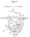
- a light irradiator 175 is disposed out of the rotating roller 102 as shown in FIG. 17. Described in more detail, the light irradiator 175 is equipped with a light emitting element 178 and a light guide prism 179, and the light emitting element 178 and the light guide prism 179 are mounted on a substrate 177 which is disposed in the housing 103 and out of the rotating roller 102.
- a surface 177a of the substrate 177 faces the light-emission face 106b of the Selfoc lens array 106, and the rotating roller 102 and the rectangular prism 157 are disposed between the surface 177a of the substrate 177 and the light-emission face 106b of the Selfoc lens array 106.
- the light guide prism 179 is designed so that light emitted from the light emitting element 178 is incident to the light-incident face 179a, the incident light is allowed to propagate to the light-emission face 179b and then the light thus propagating is emitted from the light-emission face 179b.
- the light emitted from the light-emission face 179b is incident through the rotating roller 102 to the face 157c of the rectangular prism 157 inthe direction opposite to the optical axis of the Selfoc lens array 106, propagates in the rectangular prism 157, and then is emitted from the light-incident face 157d.
- the light emitted from the light-incident face 157b is incident to the light-emission face 106b of the Selfoc lens array 106, propagates in the Selfoc lens array 106 and then is emitted from the light-incident face 106a of the Selfoc lens array 106.
- the light emitted from the light-incident face 106a of the Selfoc lens array 106 is incident to the rotating roller 102 so as to be converged to the cross portion between the optical axis of the Selfoc lens array 106 and the rotating roller 102, whereby the light is irradiated to the finger 200 pressed against the outer peripheral surface 102a of the rotating roller 102 within the image pickup window 103a.
- the image input device 171 bends the optical axis of the rectangular prism 157, whereby the inner space of the rotating roller 102 can be effectively used for the optical path from the light-emission face 106b of the Selfoc lens array 106 to the one-dimensional image pickup element 154.
- a non-film type print circuit board for example, a plastic board, a glass board, a ceramic board or the like
- a non-film type print circuit board may be used in place of the film substrates 113, 123, 133 and 143.
- a rod lens array comprising a plurality of rod lenses arranged in the form of an array, a spherical lens or other types of lenses may be used in place of the Selfoc lens array 106.
Landscapes
- Engineering & Computer Science (AREA)
- Physics & Mathematics (AREA)
- Human Computer Interaction (AREA)
- General Physics & Mathematics (AREA)
- Multimedia (AREA)
- Theoretical Computer Science (AREA)
- Optics & Photonics (AREA)
- Image Input (AREA)
- Facsimile Scanning Arrangements (AREA)
Applications Claiming Priority (4)
| Application Number | Priority Date | Filing Date | Title |
|---|---|---|---|
| JP2002180300A JP3903859B2 (ja) | 2002-06-20 | 2002-06-20 | 画像入力装置 |
| JP2002180300 | 2002-06-20 | ||
| JP2002258789A JP3941635B2 (ja) | 2002-09-04 | 2002-09-04 | 指紋画像入力装置 |
| JP2002258789 | 2002-09-04 |
Publications (3)
| Publication Number | Publication Date |
|---|---|
| EP1376447A2 true EP1376447A2 (de) | 2004-01-02 |
| EP1376447A3 EP1376447A3 (de) | 2006-01-18 |
| EP1376447B1 EP1376447B1 (de) | 2009-09-16 |
Family
ID=29718416
Family Applications (1)
| Application Number | Title | Priority Date | Filing Date |
|---|---|---|---|
| EP03013965A Expired - Lifetime EP1376447B1 (de) | 2002-06-20 | 2003-06-20 | Bildeingabevorrichtung |
Country Status (6)
| Country | Link |
|---|---|
| US (1) | US7227978B2 (de) |
| EP (1) | EP1376447B1 (de) |
| KR (1) | KR100533537B1 (de) |
| CN (1) | CN1240022C (de) |
| DE (1) | DE60329257D1 (de) |
| TW (1) | TWI232414B (de) |
Cited By (2)
| Publication number | Priority date | Publication date | Assignee | Title |
|---|---|---|---|---|
| WO2006051440A1 (en) * | 2004-11-11 | 2006-05-18 | Koninklijke Philips Electronics N.V. | Fingerprint imaging |
| EP2669843A3 (de) * | 2012-05-29 | 2015-04-15 | Fujitsu Limited | Abbildungsvorrichtung und elektronisches Gerät |
Families Citing this family (28)
| Publication number | Priority date | Publication date | Assignee | Title |
|---|---|---|---|---|
| US9092841B2 (en) | 2004-06-09 | 2015-07-28 | Cognex Technology And Investment Llc | Method and apparatus for visual detection and inspection of objects |
| JP2004206412A (ja) * | 2002-12-25 | 2004-07-22 | Casio Comput Co Ltd | カード型デバイスおよび認証システム |
| US7480397B2 (en) * | 2003-04-18 | 2009-01-20 | Casio Computer Co., Ltd. | Fingerprint image reading apparatus |
| CA2552650C (en) * | 2004-01-07 | 2014-09-30 | Identification International, Inc. | Low power fingerprint capture system, apparatus, and method |
| US8243986B2 (en) | 2004-06-09 | 2012-08-14 | Cognex Technology And Investment Corporation | Method and apparatus for automatic visual event detection |
| US20050276445A1 (en) | 2004-06-09 | 2005-12-15 | Silver William M | Method and apparatus for automatic visual detection, recording, and retrieval of events |
| US8891852B2 (en) | 2004-06-09 | 2014-11-18 | Cognex Technology And Investment Corporation | Method and apparatus for configuring and testing a machine vision detector |
| US8127247B2 (en) | 2004-06-09 | 2012-02-28 | Cognex Corporation | Human-machine-interface and method for manipulating data in a machine vision system |
| US9292187B2 (en) | 2004-11-12 | 2016-03-22 | Cognex Corporation | System, method and graphical user interface for displaying and controlling vision system operating parameters |
| US7636449B2 (en) | 2004-11-12 | 2009-12-22 | Cognex Technology And Investment Corporation | System and method for assigning analysis parameters to vision detector using a graphical interface |
| US7720315B2 (en) * | 2004-11-12 | 2010-05-18 | Cognex Technology And Investment Corporation | System and method for displaying and using non-numeric graphic elements to control and monitor a vision system |
| DE102005004640B4 (de) * | 2005-01-28 | 2009-01-29 | Cross Match Technologies Gmbh | Anordnung zur optoelektronischen Aufnahme von großflächigen Fingerabdrücken |
| JP4965151B2 (ja) * | 2006-04-11 | 2012-07-04 | ルネサスエレクトロニクス株式会社 | 固体撮像装置 |
| US7298563B1 (en) * | 2006-05-30 | 2007-11-20 | Action Electronics Co., Ltd. | Supporting member for portable digital video disk player |
| EP1993061B1 (de) * | 2007-05-16 | 2011-05-04 | Precise Biometrics AB | Sequentielle Bildausrichtung |
| US8237099B2 (en) * | 2007-06-15 | 2012-08-07 | Cognex Corporation | Method and system for optoelectronic detection and location of objects |
| US8718319B2 (en) * | 2007-06-15 | 2014-05-06 | Cognex Corporation | Method and system for optoelectronic detection and location of objects |
| US8035615B2 (en) * | 2007-11-13 | 2011-10-11 | Microsoft Corporation | User input device with ring-shaped scroll wheel |
| JP5228889B2 (ja) * | 2008-12-24 | 2013-07-03 | 富士ゼロックス株式会社 | 読取装置 |
| US9651499B2 (en) | 2011-12-20 | 2017-05-16 | Cognex Corporation | Configurable image trigger for a vision system and method for using the same |
| US8922844B2 (en) * | 2012-07-18 | 2014-12-30 | Scott C. Seifert | Cylindrical object scanner |
| WO2014152002A2 (en) * | 2013-03-15 | 2014-09-25 | Betensky Ellis I | Method and apparatus for acquiring biometric image |
| CN104579291A (zh) * | 2015-01-07 | 2015-04-29 | 江苏华途数控科技有限公司 | 一种光电波段开关 |
| KR102693504B1 (ko) * | 2016-09-26 | 2024-08-12 | 삼성디스플레이 주식회사 | 표시장치 및 그의 구동방법 |
| CN106933415B (zh) * | 2017-03-07 | 2019-11-26 | Oppo广东移动通信有限公司 | 一种传感器组件和终端 |
| KR102716356B1 (ko) * | 2019-01-25 | 2024-10-10 | 삼성전자주식회사 | 생체신호 측정용 텍스쳐 인터페이스 및 이를 포함한 생체신호 측정장치 |
| JP7083458B2 (ja) * | 2020-01-24 | 2022-06-13 | カシオ計算機株式会社 | スイッチ装置および時計 |
| CN113507544A (zh) * | 2021-08-09 | 2021-10-15 | 深圳市光太科技有限公司 | 线扫相机 |
Family Cites Families (16)
| Publication number | Priority date | Publication date | Assignee | Title |
|---|---|---|---|---|
| WO1984004614A1 (en) | 1983-05-13 | 1984-11-22 | Ira Dennis Gale | Data security device |
| US4550999A (en) * | 1984-03-05 | 1985-11-05 | Ricoh Company Ltd. | Electrophotographic copying apparatus including transfer hold-down pump |
| CA2207664A1 (en) | 1994-11-30 | 1996-06-06 | Digital Biometrics, Inc. | Apparatus and method for elimination of parallax distortion in images including palm images |
| JP3097028B2 (ja) | 1996-09-04 | 2000-10-10 | 富士通電装株式会社 | 指掌紋採取装置 |
| US6041410A (en) | 1997-12-22 | 2000-03-21 | Trw Inc. | Personal identification fob |
| US6324310B1 (en) | 1998-06-02 | 2001-11-27 | Digital Persona, Inc. | Method and apparatus for scanning a fingerprint using a linear sensor |
| JP2000048177A (ja) | 1998-07-30 | 2000-02-18 | Fujitsu Takamisawa Component Ltd | 指紋スキャナ付きカード |
| AU1474500A (en) | 1998-11-10 | 2000-05-29 | Intermedics Inc. | Cardiac lead with reduced inner crimp sleeve |
| JP2000182025A (ja) | 1998-12-14 | 2000-06-30 | Mitsubishi Plastics Ind Ltd | 指紋照合装置 |
| JP2001243444A (ja) | 2000-02-25 | 2001-09-07 | Ntt Docomo Inc | Pcカード |
| KR200189514Y1 (ko) | 2000-02-07 | 2000-07-15 | 주식회사인터넷시큐리티 | 지문 인식 기반 무전원 전자 서명 장치 |
| KR20010113916A (ko) | 2000-03-08 | 2001-12-28 | 핫토리 쥰이치 | 화상 판독장치 |
| KR20010000534A (ko) | 2000-10-05 | 2001-01-05 | 이방원 | 원통 로울러구조를 갖는 지문영상 검출장치 |
| JP3807222B2 (ja) | 2000-10-30 | 2006-08-09 | カシオ計算機株式会社 | 画像データ読み取り装置 |
| DE10111195A1 (de) | 2001-03-08 | 2002-09-19 | Infineon Technologies Ag | Vorrichtung zur Erfassung von Fingerabdrücken |
| JP2004206412A (ja) | 2002-12-25 | 2004-07-22 | Casio Comput Co Ltd | カード型デバイスおよび認証システム |
-
2003
- 2003-06-16 US US10/463,020 patent/US7227978B2/en not_active Expired - Fee Related
- 2003-06-19 TW TW092116613A patent/TWI232414B/zh not_active IP Right Cessation
- 2003-06-19 KR KR10-2003-0039644A patent/KR100533537B1/ko not_active Expired - Fee Related
- 2003-06-20 CN CNB031486185A patent/CN1240022C/zh not_active Expired - Fee Related
- 2003-06-20 DE DE60329257T patent/DE60329257D1/de not_active Expired - Lifetime
- 2003-06-20 EP EP03013965A patent/EP1376447B1/de not_active Expired - Lifetime
Cited By (2)
| Publication number | Priority date | Publication date | Assignee | Title |
|---|---|---|---|---|
| WO2006051440A1 (en) * | 2004-11-11 | 2006-05-18 | Koninklijke Philips Electronics N.V. | Fingerprint imaging |
| EP2669843A3 (de) * | 2012-05-29 | 2015-04-15 | Fujitsu Limited | Abbildungsvorrichtung und elektronisches Gerät |
Also Published As
| Publication number | Publication date |
|---|---|
| TW200404264A (en) | 2004-03-16 |
| KR100533537B1 (ko) | 2005-12-06 |
| DE60329257D1 (de) | 2009-10-29 |
| KR20030097683A (ko) | 2003-12-31 |
| TWI232414B (en) | 2005-05-11 |
| US20030235329A1 (en) | 2003-12-25 |
| EP1376447A3 (de) | 2006-01-18 |
| US7227978B2 (en) | 2007-06-05 |
| CN1240022C (zh) | 2006-02-01 |
| CN1469301A (zh) | 2004-01-21 |
| EP1376447B1 (de) | 2009-09-16 |
Similar Documents
| Publication | Publication Date | Title |
|---|---|---|
| EP1376447B1 (de) | Bildeingabevorrichtung | |
| TW499658B (en) | Method and apparatus for illuminating a fingerprint | |
| CN101257551B (zh) | 图像传感器 | |
| JP2002527832A (ja) | 指紋画像光学入力装置 | |
| TWI387902B (zh) | 光學導向裝置及光學導向方法 | |
| CN103454768B (zh) | 成像装置和电子设备 | |
| WO2014087614A1 (ja) | 画像読取装置 | |
| CN1820272A (zh) | 用于指纹识别的光学成像装置 | |
| WO2001067390A1 (en) | Image reader | |
| JP2980051B2 (ja) | 指紋検知方法および装置 | |
| JP6060937B2 (ja) | 画像読取装置 | |
| TWI439949B (zh) | 影像掃描裝置 | |
| JP3903859B2 (ja) | 画像入力装置 | |
| JP2013197606A (ja) | 画像読取装置 | |
| JP2004240924A (ja) | 指紋読取装置 | |
| CN2795945Y (zh) | 微小且薄型接触式影像感测装置 | |
| HK1062345A (en) | Image input device | |
| TWI507011B (zh) | 接觸式影像感測裝置 | |
| JP2001283207A (ja) | 画像読取り装置およびその方法およびその応用装置 | |
| TWM286425U (en) | Micro fingerprint identification module | |
| JP2004086552A (ja) | 光学素子および読取装置 | |
| JP3972827B2 (ja) | 画像入力装置 | |
| JP4395613B2 (ja) | 読取装置 | |
| JP2001283206A (ja) | 画像読取装置 | |
| TW200403596A (en) | Optical devices and optical reading apparatus |
Legal Events
| Date | Code | Title | Description |
|---|---|---|---|
| PUAI | Public reference made under article 153(3) epc to a published international application that has entered the european phase |
Free format text: ORIGINAL CODE: 0009012 |
|
| 17P | Request for examination filed |
Effective date: 20030620 |
|
| AK | Designated contracting states |
Kind code of ref document: A2 Designated state(s): AT BE BG CH CY CZ DE DK EE ES FI FR GB GR HU IE IT LI LU MC NL PT RO SE SI SK TR |
|
| AX | Request for extension of the european patent |
Extension state: AL LT LV MK |
|
| PUAL | Search report despatched |
Free format text: ORIGINAL CODE: 0009013 |
|
| AK | Designated contracting states |
Kind code of ref document: A3 Designated state(s): AT BE BG CH CY CZ DE DK EE ES FI FR GB GR HU IE IT LI LU MC NL PT RO SE SI SK TR |
|
| AX | Request for extension of the european patent |
Extension state: AL LT LV MK |
|
| 17Q | First examination report despatched |
Effective date: 20060718 |
|
| AKX | Designation fees paid |
Designated state(s): DE FR GB IT |
|
| GRAP | Despatch of communication of intention to grant a patent |
Free format text: ORIGINAL CODE: EPIDOSNIGR1 |
|
| GRAS | Grant fee paid |
Free format text: ORIGINAL CODE: EPIDOSNIGR3 |
|
| GRAA | (expected) grant |
Free format text: ORIGINAL CODE: 0009210 |
|
| AK | Designated contracting states |
Kind code of ref document: B1 Designated state(s): DE FR GB IT |
|
| REG | Reference to a national code |
Ref country code: GB Ref legal event code: FG4D |
|
| REF | Corresponds to: |
Ref document number: 60329257 Country of ref document: DE Date of ref document: 20091029 Kind code of ref document: P |
|
| PLBE | No opposition filed within time limit |
Free format text: ORIGINAL CODE: 0009261 |
|
| STAA | Information on the status of an ep patent application or granted ep patent |
Free format text: STATUS: NO OPPOSITION FILED WITHIN TIME LIMIT |
|
| 26N | No opposition filed |
Effective date: 20100617 |
|
| REG | Reference to a national code |
Ref country code: FR Ref legal event code: PLFP Year of fee payment: 14 |
|
| REG | Reference to a national code |
Ref country code: FR Ref legal event code: PLFP Year of fee payment: 15 |
|
| PGFP | Annual fee paid to national office [announced via postgrant information from national office to epo] |
Ref country code: CH Payment date: 20170912 Year of fee payment: 11 Ref country code: FR Payment date: 20170511 Year of fee payment: 15 |
|
| PGFP | Annual fee paid to national office [announced via postgrant information from national office to epo] |
Ref country code: IT Payment date: 20170619 Year of fee payment: 15 |
|
| PGFP | Annual fee paid to national office [announced via postgrant information from national office to epo] |
Ref country code: GB Payment date: 20180403 Year of fee payment: 16 |
|
| REG | Reference to a national code |
Ref country code: DE Ref legal event code: R119 Ref document number: 60329257 Country of ref document: DE |
|
| PG25 | Lapsed in a contracting state [announced via postgrant information from national office to epo] |
Ref country code: FR Free format text: LAPSE BECAUSE OF NON-PAYMENT OF DUE FEES Effective date: 20180630 Ref country code: IT Free format text: LAPSE BECAUSE OF NON-PAYMENT OF DUE FEES Effective date: 20180620 Ref country code: DE Free format text: LAPSE BECAUSE OF NON-PAYMENT OF DUE FEES Effective date: 20190101 |
|
| GBPC | Gb: european patent ceased through non-payment of renewal fee |
Effective date: 20190620 |
|
| PG25 | Lapsed in a contracting state [announced via postgrant information from national office to epo] |
Ref country code: GB Free format text: LAPSE BECAUSE OF NON-PAYMENT OF DUE FEES Effective date: 20190620 |