EP1377109A2 - Ausbaubare Architektur für einen Zugangsknoten - Google Patents
Ausbaubare Architektur für einen Zugangsknoten Download PDFInfo
- Publication number
- EP1377109A2 EP1377109A2 EP03013584A EP03013584A EP1377109A2 EP 1377109 A2 EP1377109 A2 EP 1377109A2 EP 03013584 A EP03013584 A EP 03013584A EP 03013584 A EP03013584 A EP 03013584A EP 1377109 A2 EP1377109 A2 EP 1377109A2
- Authority
- EP
- European Patent Office
- Prior art keywords
- data
- channel
- access network
- bank
- set forth
- Prior art date
- Legal status (The legal status is an assumption and is not a legal conclusion. Google has not performed a legal analysis and makes no representation as to the accuracy of the status listed.)
- Withdrawn
Links
Images




Classifications
-
- H—ELECTRICITY
- H04—ELECTRIC COMMUNICATION TECHNIQUE
- H04Q—SELECTING
- H04Q11/00—Selecting arrangements for multiplex systems
- H04Q11/04—Selecting arrangements for multiplex systems for time-division multiplexing
- H04Q11/0421—Circuit arrangements therefor
-
- H—ELECTRICITY
- H04—ELECTRIC COMMUNICATION TECHNIQUE
- H04J—MULTIPLEX COMMUNICATION
- H04J3/00—Time-division multiplex systems
- H04J3/16—Time-division multiplex systems in which the time allocation to individual channels within a transmission cycle is variable, e.g. to accommodate varying complexity of signals, to vary number of channels transmitted
- H04J3/1605—Fixed allocated frame structures
- H04J3/1611—Synchronous digital hierarchy [SDH] or SONET
-
- H—ELECTRICITY
- H04—ELECTRIC COMMUNICATION TECHNIQUE
- H04J—MULTIPLEX COMMUNICATION
- H04J2203/00—Aspects of optical multiplex systems other than those covered by H04J14/05 and H04J14/07
- H04J2203/0001—Provisions for broadband connections in integrated services digital network using frames of the Optical Transport Network [OTN] or using synchronous transfer mode [STM], e.g. SONET, SDH
- H04J2203/0028—Local loop
- H04J2203/0039—Topology
- H04J2203/0044—Bus, e.g. DQDB
-
- H—ELECTRICITY
- H04—ELECTRIC COMMUNICATION TECHNIQUE
- H04J—MULTIPLEX COMMUNICATION
- H04J2203/00—Aspects of optical multiplex systems other than those covered by H04J14/05 and H04J14/07
- H04J2203/0001—Provisions for broadband connections in integrated services digital network using frames of the Optical Transport Network [OTN] or using synchronous transfer mode [STM], e.g. SONET, SDH
- H04J2203/0046—User Network Interface
-
- H—ELECTRICITY
- H04—ELECTRIC COMMUNICATION TECHNIQUE
- H04J—MULTIPLEX COMMUNICATION
- H04J2203/00—Aspects of optical multiplex systems other than those covered by H04J14/05 and H04J14/07
- H04J2203/0001—Provisions for broadband connections in integrated services digital network using frames of the Optical Transport Network [OTN] or using synchronous transfer mode [STM], e.g. SONET, SDH
- H04J2203/0046—User Network Interface
- H04J2203/005—Terminal equipment, e.g. codecs, synch
-
- H—ELECTRICITY
- H04—ELECTRIC COMMUNICATION TECHNIQUE
- H04J—MULTIPLEX COMMUNICATION
- H04J2203/00—Aspects of optical multiplex systems other than those covered by H04J14/05 and H04J14/07
- H04J2203/0001—Provisions for broadband connections in integrated services digital network using frames of the Optical Transport Network [OTN] or using synchronous transfer mode [STM], e.g. SONET, SDH
- H04J2203/0057—Operations, administration and maintenance [OAM]
- H04J2203/006—Fault tolerance and recovery
-
- H—ELECTRICITY
- H04—ELECTRIC COMMUNICATION TECHNIQUE
- H04J—MULTIPLEX COMMUNICATION
- H04J2203/00—Aspects of optical multiplex systems other than those covered by H04J14/05 and H04J14/07
- H04J2203/0001—Provisions for broadband connections in integrated services digital network using frames of the Optical Transport Network [OTN] or using synchronous transfer mode [STM], e.g. SONET, SDH
- H04J2203/0073—Services, e.g. multimedia, GOS, QOS
- H04J2203/0082—Interaction of SDH with non-ATM protocols
-
- H—ELECTRICITY
- H04—ELECTRIC COMMUNICATION TECHNIQUE
- H04Q—SELECTING
- H04Q2213/00—Indexing scheme relating to selecting arrangements in general and for multiplex systems
- H04Q2213/13109—Initializing, personal profile
-
- H—ELECTRICITY
- H04—ELECTRIC COMMUNICATION TECHNIQUE
- H04Q—SELECTING
- H04Q2213/00—Indexing scheme relating to selecting arrangements in general and for multiplex systems
- H04Q2213/13174—Data transmission, file transfer
-
- H—ELECTRICITY
- H04—ELECTRIC COMMUNICATION TECHNIQUE
- H04Q—SELECTING
- H04Q2213/00—Indexing scheme relating to selecting arrangements in general and for multiplex systems
- H04Q2213/13178—Control signals
-
- H—ELECTRICITY
- H04—ELECTRIC COMMUNICATION TECHNIQUE
- H04Q—SELECTING
- H04Q2213/00—Indexing scheme relating to selecting arrangements in general and for multiplex systems
- H04Q2213/13216—Code signals, frame structure
-
- H—ELECTRICITY
- H04—ELECTRIC COMMUNICATION TECHNIQUE
- H04Q—SELECTING
- H04Q2213/00—Indexing scheme relating to selecting arrangements in general and for multiplex systems
- H04Q2213/1329—Asynchronous transfer mode, ATM
-
- H—ELECTRICITY
- H04—ELECTRIC COMMUNICATION TECHNIQUE
- H04Q—SELECTING
- H04Q2213/00—Indexing scheme relating to selecting arrangements in general and for multiplex systems
- H04Q2213/13292—Time division multiplexing, TDM
-
- H—ELECTRICITY
- H04—ELECTRIC COMMUNICATION TECHNIQUE
- H04Q—SELECTING
- H04Q2213/00—Indexing scheme relating to selecting arrangements in general and for multiplex systems
- H04Q2213/13298—Local loop systems, access network
-
- H—ELECTRICITY
- H04—ELECTRIC COMMUNICATION TECHNIQUE
- H04Q—SELECTING
- H04Q2213/00—Indexing scheme relating to selecting arrangements in general and for multiplex systems
- H04Q2213/1334—Configuration within the switch
-
- H—ELECTRICITY
- H04—ELECTRIC COMMUNICATION TECHNIQUE
- H04Q—SELECTING
- H04Q2213/00—Indexing scheme relating to selecting arrangements in general and for multiplex systems
- H04Q2213/13341—Connections within the switch
-
- H—ELECTRICITY
- H04—ELECTRIC COMMUNICATION TECHNIQUE
- H04Q—SELECTING
- H04Q2213/00—Indexing scheme relating to selecting arrangements in general and for multiplex systems
- H04Q2213/13349—Network management
-
- H—ELECTRICITY
- H04—ELECTRIC COMMUNICATION TECHNIQUE
- H04Q—SELECTING
- H04Q2213/00—Indexing scheme relating to selecting arrangements in general and for multiplex systems
- H04Q2213/13367—Hierarchical multiplexing, add-drop multiplexing
Definitions
- the present invention generally relates to telecommunications. More particularly, and not by way of any limitation, the present invention is directed to a scalable architecture for a telecommunications node disposed in an access network.
- the remote access market is undergoing a major metamorphosis.
- Three factors serve as catalysts for change. The first is the growing number of users, for example, small office / home office (SOHO) users, demanding high performance Internet and remote access for multimedia. Liberalized governmental activity with respect to telecommunications is another factor, which is fostering broader competition through deregulation in local area markets everywhere.
- the third and final factor is congestion in the Public Switched Telephone Network (PSTN), originally designed and developed for voice-only traffic.
- PSTN Public Switched Telephone Network
- PSN packet-switched network
- IP Internet Protocol
- CSN circuit-switched network
- next-generation network NTN
- integrated voice/data/video applications may be provisioned using a packet transport over a packet network in an end-to-end transmission path.
- NTN next-generation network
- TDM time-division multiplexed
- access networks are architected using one or more access nodes in a variety of configurations, e.g., point-to-point chains, rings, etc.
- Each access node itself comprises several channel banks that provide line interfaces servicing a large number of subscribers.
- the access nodes are typically over-designed in the sense that a high number of channel banks (e.g., upwards of 8 banks or more) are provisioned for each node at the outset.
- the internal architecture of a conventional access node is such that the banks are interconnected in a "star" configuration, with a centralized "head star” bank coupled to a plurality of satellite banks (i.e., a hub-and-spoke arrangement).
- the conventional "full-provisioning" approach to implementing an access network is beset with several disadvantages.
- the up-front cost of setting up the network can be prohibitively high.
- the increased cost structure will be particularly inefficient where only a small number of subscriber lines need to be supported intially, especially in an access node with a star architecture that is not fully populated.
- the implementation of most conventional access nodes is fraught with internal inefficiencies also, as the local data traffic within the node requires unwieldy protocol conversions.
- the local links for effectuating bank-to-bank communications are not capable of supporting the bandwidth rates necessary to implement value-added, advanced services that can be provisioned in the NGN.
- the present invention advantageously provides a scalable architecture for use with an access node terminal disposed in an access network portion, which allows incremental addition of channel banks in the node.
- a point-to-point, high-speed communication link provided between two adjacent banks of the access node logically interconnects a plurality of banks in a linear stack, thereby creating a stackplane hierarchy.
- All interbank communications i.e., traffic internal to the access node, such as data, inter-processor messaging, timing and synchronization
- SONET Synchronous Optical Network
- the payload portion of a frame is mapped to hold different types of data in their native mode, e.g., TDM, ATM, and other traffic types, and the overhead portion includes stackplane control and management information.
- the present invention is directed to access network element having a scalable architecture, comprising a primary bank including a network interface operable with a transport network and at least one node intraface operable to support a local communication link.
- the local communication link is operable to effectuate at least one full duplex data channel and at least one timing control channel in a SONET-compatible carrier.
- At least one secondary bank including a node intraface is coupled to the primary bank via the local communication link, wherein the SONET-compatible carrier includes frames with an overhead portion and a payload portion.
- the overhead portion includes a plurality of control bytes associated with the local communication link and the payload portion includes serialized data mapped to support different types of data channels.
- the present invention is directed to scalable network node for use in an access network.
- a plurality of channel banks interconnected together in a logical linear arrangement form the scalable network node, wherein one of the channel banks operates as a primary bank and the remaining channel banks operate as secondary banks.
- a first portion of the secondary banks are logically disposed on one side of the primary bank and a second portion of the secondary banks are logically disposed on the other side of the primary bank.
- the primary bank includes interfaces coupling with a transport network, e.g., a PSN, CSN, or an integrated combination thereof.
- Each of the channel banks also includes at least one node intraface card and at least cross-connect fabric card.
- the node intraface card arrangement is operable to effectuate a local communication link with at least one of its adjacent channel banks, in either direction, the local communication link supporting at least one full duplex data channel, an inter-processor messaging bus and at least one timing control channel.
- the local communication link is architected to carry interbank traffic in SONET-compatible carrier frames, wherein the payload portions can be mapped to carry serialized data traffic, e.g., TDM, ATM, etc.
- the frame overhead portions comprise a plurality of control bytes relating to the local communication link.
- the local communication link is architected with redundancy. Control software provided in the primary bank is operable to effectuate a switchover when the active communication link encounters a failure.
- FIG. 1 depicts an exemplary telecommunications network arrangement having an access network portion wherein the teachings of the present invention may be advantageously practiced;
- FIG. 2 depicts a high level conceptualization of an access network portion involving a loop carrier in conjunction with a central office
- FIG. 3 depicts an exemplary embodiment of a loop carrier system having a plurality of nodes (or, terminals) wherein the scalable architecture of the present invention may be provided in a terminal in accordance with the teachings of the present patent application;
- FIG. 4 depicts an exemplary ring topology involving multiple central office terminals (COTs);
- FIG. 5 depicts a high level block diagram of an exemplary access node terminal having the scalable architecture of the present invention, which terminal may be operable as a COT or as a remote terminal (RT) in an access network;
- FIG. 6 depicts additional details of the exemplary access node terminal shown in FIG. 5, wherein a primary bank and a plurality of secondary banks are coupled thereto via a stackplane for scalability;
- FIG. 7 depicts a functional block diagram of a portion of the exemplary access node terminal exemplifying various interfaces to effectuate the scalable stackplane architecture of the present invention
- FIG. 8 depicts a functional block diagram of an interface portion used for effectuating a high-bandwidth, bidirectional local communication link via the stackplane between two shelves or channel banks of the exemplary access node terminal;
- FIG. 9 depicts a graphical representation of the various communication channels bundled within the stackplane's local communication link
- FIG. 10 depicts an exemplary SONET-like frame used for carrier transport in the stackplane in accordance with the teachings of the present invention
- FIG. 11A depicts a functional block diagram of a primary bank's node intraface block portion for effectuating the TDM functionality in the stackplane;
- FIG. 11B depicts a functional block diagram of a secondary bank's node intraface block portion for effectuating the TDM functionality in the stackplane;
- FIG. 12A depicts a functional block diagram of a primary bank's node intraface block portion for effectuating the ATM functionality in the stackplane
- FIG. 12B depicts a functional block diagram of a secondary bank's node intraface block portion for effectuating the ATM functionality in the stackplane.
- FIG. 1 depicted therein is an exemplary network arrangement 100 having one or more access network portions, wherein the teachings of the present invention may be advantageously practiced for providing a scalable architecture for an access network element.
- the exemplary network arrangement 100 comprising a core transport network 102 and access network portions 104A and 104B, is preferably operable to support telecommunications, data communications, or any combination thereof involving diverse media such as voice, audio, video, graphics, data, and assorted multimedia.
- the core transport network 102 may be provisioned as a circuit-switched network (CSN), packet-switched network (PSN), or an integrated hybrid network capable of next-generation network (NGN) service infrastructure.
- CSN circuit-switched network
- PSN packet-switched network
- NTN next-generation network
- PSTN Public Switched Telephony Network
- PLMN Public Land Mobile Network
- the core network 102 is implemented as a packet network, it may preferably be comprised of a network operable with Internet Protocol (IP), Frame Relay, ATM, and/or other applicable technologies.
- IP Internet Protocol
- Frame Relay Frame Relay
- ATM and/or other applicable technologies.
- the access network portions 104A and 104B are disposed between end users (i.e., subscribers) exemplified by customer premises equipment (CPE) 106A, 106B, and the core network 102.
- CPE customer premises equipment
- HAN home area network
- CPE customer premises network
- PDN premises distribution network
- the CPE units may be comprised of any known or heretofore unknown Integrated Access Devices (IADs) operable with diverse media.
- IADs Integrated Access Devices
- the access network portions 104A, 104B are operable to provide remote access to the subscribers by means of various Point-of-Interface (POI) nodes and Point-of-Presence (POP) nodes interconnected via any suitable wireline, wireless, narrowband, or broadband local network.
- POI Point-of-Interface
- POP Point-of-Presence
- any suitable wireline, wireless, narrowband, or broadband local network may be implemented using well known technologies such as the Integrated Services Digital Network (ISDN), Digital Subscriber Line (DSL) and its variants, Fiber In The Loop (FITL) and its variants, Hybrid Fiber/Coaxial (HFC) cable technologies, or Wireless Local Loop (WLL) technologies.
- ISDN Integrated Services Digital Network
- DSL Digital Subscriber Line
- FITL Fiber In The Loop
- HFC Hybrid Fiber/Coaxial
- WLL Wireless Local Loop
- the exemplary access network portions 104A and 104B may be comprised of a converged local network in further embodiments of the present invention
- reference numeral 108 refers to a transaction server provided as an application node that is exemplary of a service provider operable to provide various telecom, datacom and/or integrated multimedia services to the subscribers.
- the exemplary application node 108 is illustrated as a single isolated node directly coupled to the core network 102, a private network comprising the application node 108, among others, may be provided with its own POI infrastructure in relation to the core network 102.
- the access network portion (e.g., access network 104A or 104B) is provided as a fiber-based loop carrier system that can be implemented in various embodiments depending on cost, availability of appropriate local infrastructure, services supported, etc.
- implementations such as Fiber To The Home (FTTH), Fiber To The Curb (FTTC), Fiber To The Neighborhood (FTTN), and other FITL variants may be architected as a digital loop carrier (DLC) for providing integrated, broadband access services to the subscribers.
- DLC digital loop carrier
- the fiber-based loop carrier system is preferably at least operable with a suitable physical layer infrastructure such as the Synchronous Optical Network (SONET) technology or its companion, the Synchronous Digital Hierarchy (SDH), which is similar to SONET except that its multiplexing hierarchy is a subset of the SONET multiplexing scheme.
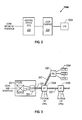
- FIG. 2 depicts a high level conceptualization of the exemplary access network portion (e.g., access network 104A) involving a loop carrier 204 in conjunction with a central office (CO) 202.
- An exemplary IAD for instance CPE 106A, is coupled to the loop carrier 204 that is operable to multiplex the access loop signal between the subscriber equipment and the CO with other loop signals.
- the POI equipment located at the CO is operable, in turn, to provide interface connectivity to the core transport network.
- the loop carrier 204 is preferably operable with a broad range of Optical Carrier (OC) signals, e.g., OC-3, OC-12, OC-48, et cetera, and the electrical equivalents corresponding thereto, namely, Synchronous Transport Signal (STS)-3, STS-12, STS-48, et cetera.
- OC Optical Carrier
- STS Synchronous Transport Signal
- STS-48 Synchronous Transport Signal
- SONET uses a synchronous transmission scheme, with a SONET frame transmitted every 125 microseconds. Each frame is logically organized as a two-dimensional array of bytes whose size is dependent on the channel rate.
- the basic SONET channel is an STS-1 (corresponding to OC-1) which consists of frames that have 810 bytes organized in 9 rows by 90 columns. At 8,000 frames per second, this gives a raw channel rate of 51.84 Mbps. Since the overhead for managing SONET line and section equipment consumes 3 of 90 columns (leaving 87 columns of payload, called the Synchronous Payload Envelope or SPE) and the path overhead typically comprises one column, a net user data rate of 49.536 Mbps (86 columns x 9 rows x 8 bits x 8000 frames/second) is available per STS-1 channel.
- SPE Synchronous Payload Envelope
- Data rates higher than STS-1 are obtained by multiplexing multiple STS-1 signals.
- three STS-1 signals can be byte-interleaved to form an STS-3 signal that operates at 155.52 Mbps.
- Another form of multiplexing is to concatenate the overhead and payload bytes of multiple STS-1 signals, for example, where an STS-3c frame contains 9 overhead columns and 261 columns for the SPE, giving rise to the data rate of 155.52 Mbps.
- an STS-n frame is an electrical signal having n-tuples of STS-1 frames which, when modulated over an optical carrier, is referred to as an OC-n optical signal.
- Transmission rates lower than STS-1 can be obtained by subdividing the payload into what are known as Virtual Tributaries (VTs) which can support data rates from Digital Signal (DS)-1 (operating at 1.544 Mbps) to DS-2 (6.312 Mbps).
- VTs Virtual Tributaries
- An STS-1 signal can be logically divided into VTs having separate identities, whereby each VT is operable to carry the same amount of payload through the fiber. Because the data within each VT retains its own ID, it can be easily separated from the rest of the STS-1 signal. Accordingly, where a loop carrier system traverses a number of nodes or sub-nodes (i.e., partitions or shelves within a node) appropriate VTs may be "dropped" at each node/sub-node for processing.
- VTs are also useful when a SONET-based access network interfaces with another network based on the Pleisochronous Digital Hierarchy (PDH) which is built upon DS-0 (64 Kbps) channels.
- PDH Pleisochronous Digital Hierarchy
- a scalable nodal architecture can be advantageously provided by utilizing a SONET-like carrier transport system in accordance with the teachings of the present invention, wherein the add/drop functionality is beneficially implemented within the context of the local (i.e., internal) inter-shelf communications as well.
- the loop carrier nodes which may also be referred to as access network nodes or terminals (more generically, telecommunications nodes), may be organized in one of several topologies for purposes of the present invention and are comprised of two forms depending on their location in the access loop.
- the loop carrier node When co-located at a CO, the loop carrier node is referred to as a central office terminal (COT).
- COT central office terminal
- Reference numeral 304 exemplifies a COT coupled to a CO switch 302 that forms part of CO 202.
- Other loop carrier nodes external to the CO are referred to as remote terminals (RTs), e.g., RT 306A and 306B.
- RTs remote terminals
- Fiber paths 305 are used for interconnecting the COT and RTs in a particular topology. Where only one RT is coupled to the COT, the resultant two-node arrangement is referred to as a point-to-point loop carrier system. On the other hand, if multiple RTs are coupled in a linear fashion, either a single feeder multiple RT (MRT) system or a dual feeder MRT system may be obtained. In a single feeder MRT system, the RTs are located on only one side of the COT, as exemplified in this FIG.
- MRT single feeder multiple RT
- the RTs are disposed on both sides of the COT, which sides are conventionally referred to as "East” and “West” sides. Accordingly, fiber optic cables emanate from the COT and run in two different directions relative thereto, each branch feeding one or more RTs.
- the loop carrier system may be arranged in a ring topology.
- a unidirectional path switched ring (UPSR) topology is obtained where the westernmost and easternmost nodes of a dual feeder MRT are connected to each other.
- UPSR path switched ring
- the East direction from the COT carries the communication traffic
- the West direction from the COT is provided as the "protect" direction in case there is a failure in the East direction cable (e.g., it is cut) or its performance degrades to a predetermined level.
- either the COT, RTs, or both may be provided with the capability to concentrate the total access lines connected thereto. That is, the total number of lines to which a terminal is connected may be greater than the maximum number of active lines supported by it. Accordingly, each terminal may have its own concentration ratio (which is the ratio between the total number of connection lines and the maximum number of active lines supported by the terminal).
- the exemplary loop carrier system may also include other equipment such as Optical Network Units (ONUs) that serve end users that are far enough away from each other that it isn't economical to connect all of them to an RT.
- the ONUs are operable to convert the signals between electrical and optical domains, if necessary.
- the ONUs digitize the analog communication signals from a plurality of customers and multiplex them onto a piece of fiber coupled to the RT.
- reference numeral 308 refers to an ONU that is coupled to RT 306A and serves, by way of example, IAD/CPE 106A.
- an RT in the loop carrier system may be coupled to one or more ONUs and RTs, in addition to the CPEs directly served by the RT.
- FIG. 4 depicts an exemplary SONET ring topology 400 involving multiple terminals.
- a plurality of COTs 402-1 through 402-4 are connected together in the ring configuration that may be implemented as an UPSR or a bidirectional line switched ring (BLSR).
- COT 402-1 is particularly exemplified with a plurality of shelves organized in a scalable architecture, wherein the primary shelf is shown with network transport interfaces 406 towards a PSN, CSN, or a combination thereof.
- a point-to-point SONET link 404 is also exemplified between the primary shelf of COT 402-1 and an RT 405.
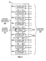
- FIG. 5 depicted therein is a high level block diagram of an exemplary access node terminal 502 operable as a COT or an RT in an access network, which terminal is provided with the scalable architecture of the present invention.
- the exemplary terminal 502 is provided as an expandable "linear stack" of a plurality of shelves or channel banks which include a primary shelf 504 and a number of secondary shelves logically disposed both above and below the primary shelf.
- the various secondary shelves are coupled to the primary shelf 504 via a redundant, bi-directional local communication link that includes appropriate inter-shelf data channel(s) and timing/control channel(s).
- FIG. 5 depicted therein is a high level block diagram of an exemplary access node terminal 502 operable as a COT or an RT in an access network, which terminal is provided with the scalable architecture of the present invention.
- the exemplary terminal 502 is provided as an expandable "linear stack" of a plurality of shelves or channel banks which include a primary shelf 504 and
- reference numerals 510 and 512 refer to the two redundant local communication links, wherein one is provided to be active while the other is operable as a standby link for effectuating protection switchover.
- the local communication links interfacing the adjacent channel banks are provided to be internal to the access node 502 and are architected to carry all the internal, full duplex data channels and timing information in SONET-type carrier frames that are mapped in accordance with the teachings of the present invention to transport the interbank communications.
- these local interfaces effectuate a logical communication plane that can be scaled in order to "stack" as many channel banks as are needed and thus may be referred to as a "stackplane” in terms of the internal architecture of the node.
- the various secondary shelves logically disposed on one side of the primary shelf 504 comprise what may be referred to as the "North" segment of the stackplane.
- secondary shelves 506-1 through 506-4 form the North stackplane segment.
- secondary shelves 508-1 through 508-4 comprise the South segment of the stackplane.
- the access node terminal 502 is provided with a plurality of subscriber interfaces 522 to which various IAD/CPEs may be coupled.
- the subscriber interfaces 522 can include subscriber interfaces 518 associated with the primary shelf 504 as well as subscriber interfaces 520 associated with secondary shelves, e.g., shelf 508-1.
- a plurality of transport network interfaces 514 and network management interfaces 516 are provided as part of the primary shelf's interfacing functionality.
- various transport networks such as a CSN, PSN, or an integrated network may be coupled to the primary channel bank 504 via the interfaces 514.
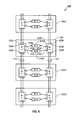
- FIG. 6 depicts a functional block diagram of a portion of the access node terminal 502 to illustrate additional details relating to the nodal stackplane architecture provided in accordance with one exemplary embodiment of the present invention.
- Each channel bank includes a pair of local interface cards for effectuating interbank communication via redundant stackplane links 510 and 512.
- these local interface cards are referred to as "node intraface" or NI cards to signify the interbank interfacing.
- the NI cards may be implemented to be compatible with an optical or electrical medium.
- the NI cards are designated as NIO cards.
- the NI cards are designated as NIE cards when implemented to be operable electrically.
- an NIx card may refer to either an NIO card or an NIE card.
- each channel bank is also provided with a pair of cross-connect fabrics implemented as switch cards (SC's).
- SC switch cards
- dual card implementation is operable to effectuate redundancy protection with respect to switch card failure.
- Each SC is operable with both NI cards of a bank via full duplex interfaces. When integrated with the bank's NI cards, however, a failure in one of the switch cards in a bank may necessitate a switchover of the node's entire active stackplane link to the standby stackplane link.
- Reference numerals 602A and 602B refer to the two NI cards (NI-A and NI-B) provided in the primary bank 504.
- Each NI card includes two stackplane (SP) interfaces - one towards the adjacent bank in one direction (e.g., the North direction) and the other towards the adjacent bank in the other direction (e.g., the South direction).
- SP stackplane
- NI-A card 602A is provided with interface 604A for coupling with the secondary channel bank 506-1 and with interface 606A for coupling with the secondary channel bank 508-1.
- NI-B card 602B includes interfaces 604B and 606B for coupling with the secondary channel banks 506-1 and 508-1, respectively.
- each NI card includes an interface towards the SC pair of the bank.
- Reference numeral 608A refers to the SC interface of NI-A card 602A towards SC-A 610A (via switch card path 614A) and SC-B 610B (via switch card path 616A) of the primary bank 504.
- NI-B card 602B is provided with interface 608B towards SC-A and SC-B cards, via switch card paths 614B and 616B, respectively.
- the stackplane interfaces provided with each channel bank allow any number of secondary banks to be added, in the North or South segments of the stackplane, on an "asneeded" basis so that the DLC nodal infrastructure can be incrementally provisioned or upgraded depending upon subscriber volume and services to be supported.
- the provision of dual redundancy, in the interbank SP links as well as internal bank switch cards, imparts a high degree of reliability to the access node architecture.
- all channel banks may use the default active stackplane (e.g., stackplane-A) and switch cards (e.g., SC-A).
- FIG. 7 shown therein is a functional block diagram of two adjacent channel banks 702A and 702B of an exemplary access node 700 that illustrates various components with respect to one of the two redundant stackplanes of the node 700.
- the two adjacent channel banks 702A and 702B are exemplary of the banks (e.g, primary bank 504 and the plurality of secondary banks coupled thereto) shown in FIGS. 5 and 6.
- Each exemplary channel bank is preferably provided with a multiplexer for multiplexing various OC-n flows.
- reference numeral 714A refers to a flow multiplexer disposed in channel bank 702A that combines OC-n flows 716A provided thereto.
- flow multiplexer 714B combines the OC-n flows 716B associated with channel bank 702B.
- the combined OC-n flow is forwarded to a DS0 multiplexer or MUX (also referred to as a space switch).
- Subscriber lines associated with the various CPE served by the channel banks are coupled to a Time Slot Interchange (TSI) that provides local switching.
- TTI Time Slot Interchange
- reference numerals 708A and 708B refer to the DS0 space switches of channel banks 702A and 702B, respectively.
- TSI 710A associated with channel bank 702A and TSI 710B associated with channel bank 702B are in a communication relationship with the respective DS0 space switches 708A and 708B.
- reference numerals 718A and 718B refer to the CPE lines serviced by channel banks 702A and 702B, respectively.
- each channel bank is provided with a local processor operable to effectuate High level Data Link Control (HDLC) communications via the stackplane by utilizing an Inter-Processor Communication (IPC) band associated therewith.
- Processors 712A and 712B are representative of the local processors associated with channel banks 702A and 702B.
- a high-level stackplane interface (SPI) block is illustrated with respect to each channel bank that is operable to effectuate (i.e., drive, receive, and convert) the various communication channels as part of the interbank stackplane communication link associated with the particular bank.
- channel banks 702A and 702B respectively include SPI blocks 704A and 704B, wherein the SPI blocks are generically representative of the NI card interfaces (e.g., interfaces 604A, 606A and 608A) shown in FIG. 6.
- SPI blocks are generically representative of the NI card interfaces (e.g., interfaces 604A, 606A and 608A) shown in FIG. 6.
- Each channel bank's DS0 MUX, TSI and local processor are accordingly interfaced to the SPI block, which provides the overall functionality associated with the NI interfaces.
- the SPI block is operable to provide a bi-directional serialization/deserialization functionality coupled with interleaving, so as to effectuate a high-speed interbank communication link 720 that comprises an upstream data path, a downstream data path and a bi-directional timing/control path.
- the interbank communication carried on SP link 720 is based on SONET technology, but without any standards-based external interfaces to the users.
- the SP link 720 is a purely internal communication link for transporting all interbank traffic (data, timing synchronization, control, IPC, internal protocol encapsulation, et cetera).
- the stackplane of an access node can be viewed as a concatenation of point-to-point, full duplex serial bus segments, running at speeds in the range of up to a few Gigabits/second.
- the SP traffic carrier format is based on SONET framing that is modified in accordance herewith for appropriately mapping the diverse traffic information into SONET frame payload (i.e., SPE).
- SONET frame payload i.e., SPE
- SONET overhead portion is utilized for SP link control and monitoring. Accordingly, although standards-compatible framing is used for the interbank traffic, it should be appreciated that it is the modified SONET (i.e., "pseudo-SONET" or SONET-compatible) frames that actually carry the traffic.
- FIG. 8 depicts a portion 800 of the SPI functional block for carrying out the serialization/deserialization functionality.
- an interleaver MUX 802 is operable with a plurality of TDM channels 806 and a plurality of ATM channels 808, which are preferably byte-interleaved.
- up to a total of 32 data channels may be interleaved.
- the interleaved data is serialized (or, deserialized in the opposite direction) by a serializer/deserializer 804 to generate serialized data 810.
- Overhead associated with serialization may also be included in the serialized data.
- FIG. 9 is a channelized view of an exemplary SP communication link 900 that provides a graphical representation of the various communication channels bundled therewith.
- Reference numerals 902 and 904 refer to the data pipes operable to carry TDM, ATM or other types of data.
- 12 STS-1 signals are utilized to carry TDM data, giving rise to a rate of 594 Mb/s that can be mapped to 8,064 DS0 channels.
- 20 STS-1 signals are used for carrying ATM data.
- the resultant bandwidth rate of 990 Mb/s can be used transport about 1.9 million ATM cells per second.
- Reference numeral 906 refers to the stackplane's IPC bus operable to carry interbank HDLC communications.
- the IPC bus is implemented as a 4 Mbps shared bus, with a hardware anti-collision scheme and a round-robin based bandwidth allocation methodology.
- the SPI block in each bank is operable to terminate the local IPC buses and extend the local IPC bus to enable the interbank processor messaging.
- Interbank timing, synchronization and control information is transported via a separate timing/control channel 908 of the SP link 900. The system timing is distributed from the primary channel bank, where preferably two redundant reference clocks reside, to the secondary channel banks.
- SONET-compliant frame 1000 used for carrier transport in the stackplane in accordance with the teachings of the present invention.
- a plurality of frames such as frame 1000 are interleaved into a superframe carrier for the stackplane.
- SONET-compliant frame 1000 includes an overhead portion 1004 and a payload (SPE) portion 1002.
- SPE payload
- the three columns, each byte wide, of the overhead portion 1004 are particularly exemplified herein, which include stackplane control information for purposes of the present invention.
- Bytes A1, A2, B1, and H1-H3 are valid SONET bytes used in accordance with the GR-253-CORE standard.
- the carrier payload type is indicated by a Payload Type Identifier (PTI) byte.
- PTI Payload Type Identifier
- $0F indicates TDM data
- $F0 indicates ATM data in the SPE.
- the active status of the stackplane is defined by A/S* byte, where $0F indicates that the stackplane is in standby mode and SFO indicates that the stackplane is active. This byte is used only in the first STS-1 frame of a superframe (e.g., an STS-12 superframe). Furthermore, the A/S* byte is used in the egress direction only.
- ADRS bank address
- SSD Protection Switching Diagnostics
- HC* Hop Count
- this byte may also be used to detect a change in the topology of a node's stackplane architecture as it is modified, upgraded, etc.
- a request/grant (R/G) byte is used to implement an anti-collision scheme for the IPC messaging on the stackplane (i.e., avoidance/resolution of the IPC bus contention).
- R/G request/grant
- Up to six IPC bytes are provided with respect to interbank HDLC link data and control.
- Frame offset (FO*) and superframe offset (SFO*) information is provided as part of an alignment protocol used for the stackplane.
- the various SP control bytes set forth above are defined for both egress and ingress directions (in relation to the primary bank), except as otherwise noted.
- ADRS and PSD bytes are used only in the ingress direction, whereas A/S* byte is valid in the egress direction only.
- a * symbol is used to denote where the control byte defined in the first STS-1 frame only. If the * symbol is not used, then the control byte is used in each STS-1 frame of the superframe carrier.
- the SPE portion 1002 of frame 1000 is used for mapping appropriate data channels.
- the stackplane link can be viewed as a high-speed shared bus between the banks, with no anti-collision scheme (i.e., a bank may overwrite the data written on the TDM band by another bank).
- the stackplane link is a shared bus between the banks, but with a master (e.g., the active ATM cross-connect fabric in the primary bank) and an anti-collision scheme (i.e., a suitable request/grant protocol is used).
- a payload capacity of up to 20 STS-1 frames may be provisioned.
- an overhead containing the ATM request/grant protocol bits and bank destination address may be added to each ATM cell transported by the stackplane carrier. In one packaging scheme, up to 12 ATM cells are mapped to the SPE portion 1002.
- a port is built upon the Physical Layer, and is created within the NIx cards preferably by the duplex pairing of Layer 1 components.
- a protocol is introduced to establish a duplex link (also a Link Layer 2 component) over the media spanned between the ports.
- Layer 2 entities of the present invention are roughly analogous to the section equipment of a SONET system.
- a chain (Network Layer 3 component) is built upon the Link Layer ports, links and underlying media, and supports an extension of network services throughout the stackplane.
- the SP structure provides for the inbound and outbound flow of Network Layer 3 data (ATM cells and TDM DS-n packets) across a plurality of chains within the node.
- Layer 3 entities can be equated with the line components of a SONET system.
- a path (Transport Layer 4 component) is built upon the Network Layer 3 chains (or sub-nets), and routes the network traffic through a cross-connect fabric of the node. Layer 4 entities are analogous with the path components of a SONET system.
- stackplane exists as a Layer 1 - Layer 3 structure with respect to an access node and provides a scalable architecture that advantageously allows incremental addition of banks with minimal downtime, cost and administration oversight.
- the following discussion now focuses on the various NIx interfaces provided as part of an exemplary stackplane implementation.
- FIG. 11A depicts a functional block diagram of a primary bank's NIx block portion 1100A for effectuating the TDM transport functionality in a stackplane.
- a pair of serializer/deserializer blocks 1102A and 1102B are provided, one with respect to the North-facing stackplane segment and the other with respect to the South-facing stackplane segment, for serializing the egress data (i.e., data going out from the bank) and for deserializing the ingress data (i.e., data coming into the bank).
- another pair of serializer/deserializer blocks 1104A and 1104B are included for interfacing with the redundant switch card paths.
- a MUX 1106 is operable to multiplex and de-multiplex the TDM data that is going out on, or received from, the switch card paths, respectively.
- the data received from the bank's switch card paths is de-muxed by MUX 1108, which de-muxed data is sent to a plurality of MUX units controlled by control memory software.
- MUX 1120 multiplexes the data from the switch card paths and the deserialized ingress data from the North-facing stackplane segment under the auspices of control memory 1126. Output from MUX 1120 is provided to another MUX 1122 operating under a control memory 1124.
- the output from MUX 1122 is operable to be sent to be sent out on the South-facing stackplane segment (via serializer 1102B) for egress transport. Or, a part of the output (including data to be locally routed or data received from the North-facing stackplane and bound for subscriber lines local to the primary bank) may be sent out on the switch card paths via MUX 1114 and MUX 1116 which operate under control memories 1112 and 1118, respectively.
- data received from the South-facing stackplane is deserialized and provided to MUX 1132 operating under the control of control memory 1128, which MUX is also operable to multiplex the data received from the bank's switch card paths via MUX 1108.
- Output from MUX 1132 is provided to MUX 1134 which operates under the control of control memory 1130 and multiplexes the data received on the inbound switch card paths, analogous to MUX 1122 operating under control memory 1124.
- the output from MUX 1134 can be sent out on the egress path of the North-facing stackplane via serializer 1102A, or a portion of it can be sent out (including data to be locally routed or data received from the South-facing stackplane and bound for subscriber lines local to the primary bank) on the outbound switch card paths via MUX 1114/1116, MUX 1110, and the redundant serializer interface 1104A/1104B.
- MUX/DE-MUX combinations and associated control memory software are operable to effectuate the TSI functionality for local routing and/or for pass-through routing, and may be implemented in a suitable field-programmable gate array device.
- FIG. 11B depicts a functional block diagram of a secondary bank's NIx block portion 1100B for effectuating the stackplane's TDM transport functionality. It should be readily apparent upon having reference hereto that the NIx block 1100B for a secondary bank is similar to that of the primary bank, with its own control memories for DS0 insertion and extraction.
- MUX 1150 controlled by control memory 1152 is operable for sending out data on secondary bank's switch card paths via serializer interfaces 1104A and 1104B.
- MUX 1154 controlled by control memory 1156 is operable to send out data on the South-facing stackplane, or a portion of the data may be looped back to MUX 1150.
- MUX 1164 controlled by control memory 1162 is operable to send out data on the North-facing stackplane, or a portion thereof may be provided to MUX 1150.
- appropriate delay blocks are also provided. For instance, delay 1158 is inserted into the inbound data received on the switch card paths. Another delay 1160 is provided between MUX 1164 and MUX 1150.
- FIG. 12A shown therein is a functional block diagram of a primary bank's NIx block 1200A for effectuating the stackplane's ATM transport functionality.
- the NIx's ATM functions include: (i) serialization and deserialization for both stackplane and switch card interfacing, (ii) payload extraction from ingress paths of the North- and South-facing stackplanes, (iii) queue merging for data received from the switch card paths, (iv) cell buffering, and (v) egress copy selection and cell routing.
- Payload extractors 1208A and 1208B are operable to extract ATM cells from the inbound data received on the North-facing and South-facing stackplanes, respectively.
- the extracted data is queued into in queues 1210A and 1210B before getting merged by MUX 1206.
- Output from MUX 1206 is first buffered in buffers 1202A and 1202B and then sent out to the switch card paths via serializer interfaces 1104A and 1104B.
- deserialized ATM data received on the switch card paths is buffered in buffers 1202A and 1202B.
- Egress cell routing is then effectuated by block 1204, which provides the outbound ATM data to serializers 1102A and 1102B for transporting on the North and/or South stackplane segments.
- FIG. 12B depicts a functional block diagram of a secondary bank's NIx block portion 1200B for effectuating the ATM transport functionality of the stackplane. While essentially similar to the ATM functionality of a primary bank's NIx card, the ATM functionality of the NIx card 1200B includes additional aspects such as ingress cell injection, SONET framing, Destination Route Tag (DRT) filtering, and end of chain loopback.
- DVT Destination Route Tag
- Deserialized ATM data received on the North-facing stackplane is first provided to a framer/DRT filter block 1258 whose output can be routed to: (i) buffers 1202A/1202B for sending out on the switch card paths, (ii) serializer 1102B directly, for sending out on the egress path of the South-facing stackplane, or (iii) a MUX 1254 operable to multiplex the loopback path with framed data received from the ingress path of the South-facing stackplane.
- Framer 1252 is operable to provide SONET framing for the ingress data on the South stackplane segment.
- Deserialized ATM data received on the switch card paths is buffered in buffers 1202A/1202B and then multiplexed by MUX 1250.
- Outputs generated by MUX 1254 and MUX 1250 are provided to a control block 1256 operable to perform cell insertion and request insertion. Thereafter, upon serializing the ATM cells, the serial data is sent out on the North-facing stackplane.
- the present invention advantageously provides an innovative access node architecture that affords efficient scalability.
- the internal stackplane hierarchy supports a linear chain of inter-connected banks that can be concatenated with minimal effort and downtime, thereby allowing a network operator to incrementally add extra infrastructure.
- Interbank stackplane links can be effectuated either on copper wire media for shorter distances (less than about 10 meters) or by using a fiber.
- the scalable provisioning of hardware supported by the stackplane architecture in accordance with the teachings of the present invention advantageously affords a cost-effective business model for providing additional, value-added services (involving real time video (e.g., video-on-demand), data, graphics, and multimedia), which spreads the risk factors associated with service provisioning on a broader horizon.
- additional, value-added services involving real time video (e.g., video-on-demand), data, graphics, and multimedia
Landscapes
- Engineering & Computer Science (AREA)
- Computer Networks & Wireless Communication (AREA)
- Signal Processing (AREA)
- Time-Division Multiplex Systems (AREA)
Applications Claiming Priority (2)
| Application Number | Priority Date | Filing Date | Title |
|---|---|---|---|
| US18438602A | 2002-06-27 | 2002-06-27 | |
| US184386 | 2002-06-27 |
Publications (2)
| Publication Number | Publication Date |
|---|---|
| EP1377109A2 true EP1377109A2 (de) | 2004-01-02 |
| EP1377109A3 EP1377109A3 (de) | 2004-06-16 |
Family
ID=29717959
Family Applications (1)
| Application Number | Title | Priority Date | Filing Date |
|---|---|---|---|
| EP03013584A Withdrawn EP1377109A3 (de) | 2002-06-27 | 2003-06-14 | Ausbaubare Architektur für einen Zugangsknoten |
Country Status (1)
| Country | Link |
|---|---|
| EP (1) | EP1377109A3 (de) |
Family Cites Families (2)
| Publication number | Priority date | Publication date | Assignee | Title |
|---|---|---|---|---|
| EP1104644A4 (de) * | 1998-08-18 | 2009-07-29 | Alcatel Usa Sourcing Lp | Plattform mit gemeinsamen zugriff |
| US7050428B1 (en) * | 1999-12-22 | 2006-05-23 | Alcatel | Stackplane architecture |
-
2003
- 2003-06-14 EP EP03013584A patent/EP1377109A3/de not_active Withdrawn
Also Published As
| Publication number | Publication date |
|---|---|
| EP1377109A3 (de) | 2004-06-16 |
Similar Documents
| Publication | Publication Date | Title |
|---|---|---|
| EP1376915B1 (de) | Verfahren und System zur Taktsynchronisierung in einem ausbaubaren Zugangsknoten | |
| US5355362A (en) | Digital loop carrier system | |
| US6768745B1 (en) | Flexible SONET access and transmission system | |
| US6667973B1 (en) | Flexible SONET access and transmission systems | |
| US5436890A (en) | Integrated multi-rate cross-connect system | |
| US6317439B1 (en) | Architecture for a SONET line unit including optical transceiver, cross-connect and synchronization subsystem | |
| US6359859B1 (en) | Architecture for a hybrid STM/ATM add-drop multiplexer | |
| US6816496B2 (en) | Frame based data transmission over synchronous digital hierarchy network | |
| US6798784B2 (en) | Concurrent switching of synchronous and asynchronous traffic | |
| US6697373B1 (en) | Automatic method for dynamically matching the capacities of connections in a SDH/SONET network combined with fair sharing of network resources | |
| US5809022A (en) | Method and apparatus for converting synchronous narrowband signals into broadband asynchronous transfer mode signals | |
| US20070280223A1 (en) | Hybrid data switching for efficient packet processing | |
| US7130276B2 (en) | Hybrid time division multiplexing and data transport | |
| US6671271B1 (en) | Sonet synchronous payload envelope pointer control system | |
| CN101754063B (zh) | 用于交换时分复用信号的网元和方法 | |
| US20040037290A1 (en) | Switching device for telecommunication networks | |
| US6292485B1 (en) | In-band management control unit software image download | |
| US6658006B1 (en) | System and method for communicating data using modified header bits to identify a port | |
| US7031324B1 (en) | Local area network/wide area network switch | |
| US6580709B1 (en) | Sonet system and method which performs TSI functions on the backplane and uses PCM buses partitioned into 4-bit wide parallel buses | |
| JP2004535111A (ja) | チャネライズされたイーサネットをsonet/sdhを介して伝送するシステム及び方法 | |
| US20050068993A1 (en) | Frame based data transmission over synchronous digital hierarchy network | |
| EP1701467B1 (de) | Zuführungseinheit einer synchronen digitalen hierarchie und eines sdh-vorrichtungsknoten | |
| US7139255B1 (en) | Bandwidth grooming functionality in an access network element | |
| US7142549B2 (en) | Digital hierarchy based communication systems |
Legal Events
| Date | Code | Title | Description |
|---|---|---|---|
| PUAI | Public reference made under article 153(3) epc to a published international application that has entered the european phase |
Free format text: ORIGINAL CODE: 0009012 |
|
| AK | Designated contracting states |
Kind code of ref document: A2 Designated state(s): AT BE BG CH CY CZ DE DK EE ES FI FR GB GR HU IE IT LI LU MC NL PT RO SE SI SK TR |
|
| AX | Request for extension of the european patent |
Extension state: AL LT LV MK |
|
| PUAL | Search report despatched |
Free format text: ORIGINAL CODE: 0009013 |
|
| AK | Designated contracting states |
Kind code of ref document: A3 Designated state(s): AT BE BG CH CY CZ DE DK EE ES FI FR GB GR HU IE IT LI LU MC NL PT RO SE SI SK TR |
|
| AX | Request for extension of the european patent |
Extension state: AL LT LV MK |
|
| 17P | Request for examination filed |
Effective date: 20041214 |
|
| AKX | Designation fees paid |
Designated state(s): AT BE BG CH CY CZ DE DK EE ES FI FR GB GR HU IE IT LI LU MC NL PT RO SE SI SK TR |
|
| RAP1 | Party data changed (applicant data changed or rights of an application transferred) |
Owner name: ALCATEL LUCENT |
|
| 17Q | First examination report despatched |
Effective date: 20070320 |
|
| STAA | Information on the status of an ep patent application or granted ep patent |
Free format text: STATUS: THE APPLICATION IS DEEMED TO BE WITHDRAWN |
|
| 18D | Application deemed to be withdrawn |
Effective date: 20070731 |