EP1377122A2 - Verzögerungseinheit für Tondaten - Google Patents
Verzögerungseinheit für Tondaten Download PDFInfo
- Publication number
- EP1377122A2 EP1377122A2 EP03253505A EP03253505A EP1377122A2 EP 1377122 A2 EP1377122 A2 EP 1377122A2 EP 03253505 A EP03253505 A EP 03253505A EP 03253505 A EP03253505 A EP 03253505A EP 1377122 A2 EP1377122 A2 EP 1377122A2
- Authority
- EP
- European Patent Office
- Prior art keywords
- sound data
- channel
- memory
- address
- address information
- Prior art date
- Legal status (The legal status is an assumption and is not a legal conclusion. Google has not performed a legal analysis and makes no representation as to the accuracy of the status listed.)
- Ceased
Links
Images




Classifications
-
- G—PHYSICS
- G06—COMPUTING OR CALCULATING; COUNTING
- G06F—ELECTRIC DIGITAL DATA PROCESSING
- G06F5/00—Methods or arrangements for data conversion without changing the order or content of the data handled
- G06F5/06—Methods or arrangements for data conversion without changing the order or content of the data handled for changing the speed of data flow, i.e. speed regularising or timing, e.g. delay lines, FIFO buffers; over- or underrun control therefor
- G06F5/065—Partitioned buffers, e.g. allowing multiple independent queues, bidirectional FIFO's
-
- H—ELECTRICITY
- H04—ELECTRIC COMMUNICATION TECHNIQUE
- H04S—STEREOPHONIC SYSTEMS
- H04S1/00—Two-channel systems
- H04S1/007—Two-channel systems in which the audio signals are in digital form
-
- G—PHYSICS
- G06—COMPUTING OR CALCULATING; COUNTING
- G06F—ELECTRIC DIGITAL DATA PROCESSING
- G06F2205/00—Indexing scheme relating to group G06F5/00; Methods or arrangements for data conversion without changing the order or content of the data handled
- G06F2205/06—Indexing scheme relating to groups G06F5/06 - G06F5/16
- G06F2205/066—User-programmable number or size of buffers, i.e. number of separate buffers or their size can be allocated freely
-
- H—ELECTRICITY
- H04—ELECTRIC COMMUNICATION TECHNIQUE
- H04S—STEREOPHONIC SYSTEMS
- H04S3/00—Systems employing more than two channels, e.g. quadraphonic
- H04S3/008—Systems employing more than two channels, e.g. quadraphonic in which the audio signals are in digital form, i.e. employing more than two discrete digital channels
Definitions
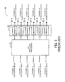
- the maximum value of the delay amount for each channel is determined on the basis of the capacity of each of the memories 32-0 to 32-5. Therefore, even if the memory capacity is not used to the maximum in some channels, in other words, no matter how much extra memory capacity is left in some channels, it is not possible to utilize the area of the extra memory capacity for the other channels. Consequently, it is required to provide the capacity in accordance with the maximum value of the delay amount that all the memories of all the channels can carry.
- a sound data delay unit (audio signal delay processor) 10 comprises a memory 1 for temporarily storing sound data such as PCM data, address information generators 2-0 to 2-n (n is a natural number other than 0) for generating address information for assigning a sound data storage area for each channel, a selector 3 for selecting from a plurality of channels the sound data to be input into the memory 1, a selector 4 for selecting the address information to be input into the memory 1, a distributor 5 for distributing to each channel the sound data stored in the memory 1 and corresponding to the respective channels, and a controller 6 for controlling the memory 1, the selector 3, the selector 4 and the distributor 5.
- the address information generators 2-0 to 2-n When sound data is input through the channels 0 to n into the selector 3, the address information generators 2-0 to 2-n generate the address information for assigning the storage areas for storing the sound data in the memory 1 on the basis of the delay amount input through each channel, and input the address information into the selector 4 under the control of the controller 6.
- the selector 4, under the control of the controller 6, selects the address information in the address information generators 2-0 to 2-n, inputs the address information into the memory 1, and assigns the storage area for temporarily storing the sound data of each channel.
- the selector 3 selects the channels to be input into the memory 1, the sound data is input into the storage areas assigned on the basis of the address information with respect to each channel under the control of the controller 6.
- channels are not provided each with a respective memory to delay sound data, but the sound data of the channels is stored in the single memory 1 by using the address information generated on the basis of the delay amount assigned to each channel. Therefore, it is possible to use memory capacity effectively.
- Fig. 2 illustrates the structure of the sound data delay unit according to the embodiment of the present invention.
- a sound data delay unit 20 comprises a memory 21 for temporarily storing sound data, address counters 22-0 to 22-n receiving the delay amount assigned to each channel, and based on the delay amount, generating the address information for assigning a sound data storage area for each channel in the memory 21, a multiplexer 23 for selecting the sound data to be input into the memory 21 from the channels, a multiplexer 24 for selecting the address information to be input into the memory 21, a demultiplexer 25 for distributing to each channel the sound data stored in the memory 21 and corresponding to the respective channels, filters 26-0 to 26-n for smoothing the sound data which has been distributed and retrieved, selectors 27-0 to 27-n for determining whether or not outputs have passed through the respective filters 26-0 to 26-n, and a control circuit 28 for controlling the memory 21, the multiplexers 23 and 24, the demultiplexer 25, and the selectors 27-0 to 27-n.
- the sound data delay unit 20 with the above structure is part of, for example, a decoder chip in a DVD player.
- the channels for the sound data to be input are connected to, for instance, a DSP, not shown, and the sound data decoded into PCM data in the DSP are input into the sound data delay unit 20.
- the memory 21 corresponds to the memory 1 shown in Fig. 1, the address counters 22-0 to 22-n to the address information generators 2-0 to 2-n in Fig. 1, the multiplexer 23 to the selector 3, the multiplexer 24 to the selector 4, the demultiplexer 25 to the distributor 5, and the control circuit 28 to the controller 6.
- the memory 21 is connected with the multiplexers 23 and 24, the demultiplexer 25 and the control circuit 28, and has a function of temporarily storing the sound data input from the multiplexer 23 in the address assigned by the multiplexer 24, under the control of the control circuit 28. Moreover, the memory 21 has another function of outputting the stored sound data to the demultiplexer 25 under the control of the control circuit 28.
- the address counters 22-0 to 22-n generate the address information for assigning the storage areas for temporarily storing the sound data in the memory 21, based on the delay amount input through each channel. Details will be described below.
- the delay amount can be appropriately determined with respect to each channel. For instance, a user or the like may delay a channel 0 for 1 msec, and a channel 1 for 2 msec by operating an input unit, not shown.
- the determined delay time is stored in a register or the like, not shown.
- the sound data is input into the multiplexer 23 through the channels, and the multiplexer 23 selects channels and inputs the corresponding sound data into the memory 21 under the control of the control circuit 28.
- the multiplexer 24 selects the address information generated by the address counters 22-0 to 22-n corresponding to the respective channels and inputs the address information into the memory 21.
- the filters 26-0 to 26-n have a function of smoothing the sound to be output based on the sound data.
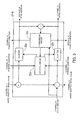
- Fig. 3 shows the structure of the address counter.
- the address counter 22-N includes counters 22a and 22b, a comparison circuit 22c, and a control circuit 22d.
- the sound data is temporarily stored in the memory 21 to be delayed.
- the address counter 22-N generates the address information for assigning the storage area for storing the sound data of a channel N within the memory 21.
- the address information includes a write address, a read address, and a write and a read pointer indicative of these addresses.
- the counter 22a operates under the control of the control circuit 22d and brings the read pointer to increment.
- the counter 22b operates under the control of the control circuit 22d and brings the write pointer to increment.
- the control circuit 22d controls the counters 22a and 22b and receives the pointer conditions of the adjacent address counters 22-(N - 1) and 22-(N + 1). Also, the control circuit 22d receives the result of the comparison made by the comparison circuit 22c.
- Fig. 4 is a diagram showing connections of the address counters and sending and receiving of the address information.
- the address counter 22-1 receives the initial value of the write address of the channel 0, the pointer condition of the channel 0 and the pointer condition of a channel 2, sends the pointer condition of the channel 1 to the channel 0, and sends the initial value of the write address of the channel 1 and the pointer condition of the channel 1 to the channel 2.
- the address counter 22-2 operates in the same manner as the address counter 22-1.
- the last address counter 22-n receives the initial value of the write address and the pointer condition from an address counter 22-(n - 1), and sends the pointer condition of an address counter 22-n to the address counter 22-(n - 1).
- the write address initial value of the channel N - 1 is input from the address counter 22-(N - 1) antecedent to the address counter 22-N, and the initial value incremented by 1 becomes the read pointer of the channel N.
- the read pointer is output as the read address of the channel N via the counter 22a.
- the write pointer of the channel N is obtained by adding to the channel 1 read pointer the data area corresponding to the delay amount of the channel N input from without and stored in, for example, a register, not shown. In the case of the initial state, the write pointer is output as the write address of the channel N via the counter 22b.
- the multiplexer 24 selects the read address and write address of each channel, which have been generated in the address counters 22-0 to 22-n, with respect to each channel and inputs the selected address into the memory 21 under the control of the control circuit 28.
- Channel storage areas of the memory 21 in the initial state which are assigned on the basis of the read and write addresses as mentioned above, will be described below.
- Fig. 5 shows the storage areas of the memory in the initial state.
- the areas for storing the sound data for each channel within the memory 21 are produced, the areas including the storage area of the channel 0 as a first area specified by the read address represented as read pointer RD-0 of the channel 0 and the write address represented as write pointer WR-0 of the channel 0 and the storage area of the channel n as a last area specified by the read address represented as read pointer RD-n of the channel n and the write address represented as write pointer WR-n of the channel n.
- An arrow on the right side on Fig. 5 indicates an address direction.
- Difference between the write pointer WR-0 and the read pointer RD-0 shows the delay amount of the channel 0, whereas difference between the write pointer WR-1 and the read pointer RD-1 indicates the delay amount of the channel 1. Moreover, difference between the write pointer WR-n and the read pointer RD-n shows the delay amount of the channel n.
- the increment of the write pointer or read pointer is restored to the normal operation. Furthermore, during the change of the delay amount, the output from the memory 21 is discontinued. Therefore, while the delay amount is being altered, the outputs passing through the filters 26-0 to 26-n are selected by the selectors 27-0 to 27-n under the control of the control circuit 28 and subjected to a smoothing process in the filters 26-0 to 26-n. Then, the output is carried out (i.e. sound is generated from the sound data).
- the counters 22a and 22b increment each pointer by 1 in synchronization with the input data.
- the write pointer is incremented by 1 in the counter 22b in synchronization with the input data as usual.
- the read pointer is incremented by 1 in the counter 22a in synchronization with the input data as usual.
- the increment of the read pointer of the channel N is brought to a halt so that the gap may not be produced.
- the present invention is designed to perform the delay of multiple audio channels in a single memory 21. Therefore, when the delay amount of one of the channels is small, it is possible to set the delay amount of the other channels to be large. Thus, usability of the memory is heightened.
Landscapes
- Engineering & Computer Science (AREA)
- Physics & Mathematics (AREA)
- Theoretical Computer Science (AREA)
- General Engineering & Computer Science (AREA)
- General Physics & Mathematics (AREA)
- Multimedia (AREA)
- Acoustics & Sound (AREA)
- Signal Processing (AREA)
- Electrophonic Musical Instruments (AREA)
- Stereophonic System (AREA)
Applications Claiming Priority (2)
| Application Number | Priority Date | Filing Date | Title |
|---|---|---|---|
| JP2002187931A JP2004032513A (ja) | 2002-06-27 | 2002-06-27 | 音声データ遅延装置 |
| JP2002187931 | 2002-06-27 |
Publications (2)
| Publication Number | Publication Date |
|---|---|
| EP1377122A2 true EP1377122A2 (de) | 2004-01-02 |
| EP1377122A3 EP1377122A3 (de) | 2006-09-06 |
Family
ID=29717648
Family Applications (1)
| Application Number | Title | Priority Date | Filing Date |
|---|---|---|---|
| EP03253505A Ceased EP1377122A3 (de) | 2002-06-27 | 2003-06-04 | Verzögerungseinheit für Tondaten |
Country Status (3)
| Country | Link |
|---|---|
| US (1) | US20040001596A1 (de) |
| EP (1) | EP1377122A3 (de) |
| JP (1) | JP2004032513A (de) |
Families Citing this family (3)
| Publication number | Priority date | Publication date | Assignee | Title |
|---|---|---|---|---|
| KR100868935B1 (ko) * | 2006-12-18 | 2008-11-17 | 대한민국 | 유색 현미(흑진주미)를 이용한 무증자 양조식초 제조법 |
| US20080151765A1 (en) * | 2006-12-20 | 2008-06-26 | Sanal Chandran Cheruvathery | Enhanced Jitter Buffer |
| JP5511961B2 (ja) * | 2009-09-03 | 2014-06-04 | ローベルト ボツシユ ゲゼルシヤフト ミツト ベシユレンクテル ハフツング | 会議オーディオシステム用の遅延ユニット、オーディオ入力信号を遅延する方法、コンピュータプログラムおよび会議オーディオシステム |
Family Cites Families (6)
| Publication number | Priority date | Publication date | Assignee | Title |
|---|---|---|---|---|
| US4581759A (en) * | 1983-06-30 | 1986-04-08 | Nippon Gakki Seizo Kabushiki Kaisha | Signal delaying device |
| US4672473A (en) * | 1984-02-13 | 1987-06-09 | Victor Company Of Japan, Ltd. | Audiovisual disc recording |
| JP2961792B2 (ja) * | 1990-03-16 | 1999-10-12 | 日本電気株式会社 | Ramアドレス生成回路 |
| US5406518A (en) * | 1994-02-08 | 1995-04-11 | Industrial Technology Research Institute | Variable length delay circuit utilizing an integrated memory device with multiple-input and multiple-output configuration |
| US6085309A (en) * | 1997-01-08 | 2000-07-04 | Yamaha Corporation | Signal processing apparatus |
| JP3661556B2 (ja) * | 2000-03-22 | 2005-06-15 | ヤマハ株式会社 | 楽音信号処理装置 |
-
2002
- 2002-06-27 JP JP2002187931A patent/JP2004032513A/ja active Pending
-
2003
- 2003-06-04 EP EP03253505A patent/EP1377122A3/de not_active Ceased
- 2003-06-11 US US10/458,193 patent/US20040001596A1/en not_active Abandoned
Also Published As
| Publication number | Publication date |
|---|---|
| US20040001596A1 (en) | 2004-01-01 |
| JP2004032513A (ja) | 2004-01-29 |
| EP1377122A3 (de) | 2006-09-06 |
Similar Documents
| Publication | Publication Date | Title |
|---|---|---|
| JP4620133B2 (ja) | オーディオオブジェクトを用いて波面合成レンダラ手段を制御するための装置および方法 | |
| US6665409B1 (en) | Methods for surround sound simulation and circuits and systems using the same | |
| US3969588A (en) | Audio pan generator | |
| JP2008532373A (ja) | 波面合成システムをシミュレートするための装置および方法 | |
| US4581759A (en) | Signal delaying device | |
| JP4998046B2 (ja) | 楽音発生装置 | |
| JP4547009B2 (ja) | 波面合成レンダリング手段を制御するための装置および方法 | |
| US20030126975A1 (en) | Electronic musical instrument | |
| JP2013504229A (ja) | 会議オーディオシステム用の遅延ユニット、オーディオ入力信号を遅延する方法、コンピュータプログラムおよび会議オーディオシステム | |
| JPH03192296A (ja) | 電子楽器 | |
| US4268717A (en) | Time-modulated delay system and improved reverberation simulator using same | |
| US4937875A (en) | Audio signal processing apparatus | |
| US20040001596A1 (en) | Sound data delay unit | |
| US4303991A (en) | Time-modulated delay system | |
| US7474753B2 (en) | Sound field control apparatus, signal processing apparatus, sound field control program, and signal processing program | |
| CA2134308C (en) | Audio synthesizer time-sharing its first memory unit between two processors | |
| JP2002058100A (ja) | 音像定位制御装置および音像定位制御プログラムが記録された記録媒体 | |
| US6031916A (en) | Sound effect adding device using DSP | |
| JPH0828913B2 (ja) | 時間多重スイッチ | |
| JP2921286B2 (ja) | デジタルトーン発生回路 | |
| JP3358707B2 (ja) | 楽音生成装置 | |
| JPH0231890B2 (de) | ||
| JP3671756B2 (ja) | 音場再生装置 | |
| JP4123090B2 (ja) | 音場制御装置 | |
| JP4123091B2 (ja) | 音場制御装置 |
Legal Events
| Date | Code | Title | Description |
|---|---|---|---|
| PUAI | Public reference made under article 153(3) epc to a published international application that has entered the european phase |
Free format text: ORIGINAL CODE: 0009012 |
|
| AK | Designated contracting states |
Kind code of ref document: A2 Designated state(s): AT BE BG CH CY CZ DE DK EE ES FI FR GB GR HU IE IT LI LU MC NL PT RO SE SI SK TR |
|
| AX | Request for extension of the european patent |
Extension state: AL LT LV MK |
|
| PUAL | Search report despatched |
Free format text: ORIGINAL CODE: 0009013 |
|
| AK | Designated contracting states |
Kind code of ref document: A3 Designated state(s): AT BE BG CH CY CZ DE DK EE ES FI FR GB GR HU IE IT LI LU MC NL PT RO SE SI SK TR |
|
| AX | Request for extension of the european patent |
Extension state: AL LT LV MK |
|
| RIC1 | Information provided on ipc code assigned before grant |
Ipc: H04S 3/00 20060101ALN20060803BHEP Ipc: G06F 5/06 20060101ALI20060803BHEP Ipc: H04S 1/00 20060101AFI20031008BHEP |
|
| 17P | Request for examination filed |
Effective date: 20070102 |
|
| 17Q | First examination report despatched |
Effective date: 20070209 |
|
| AKX | Designation fees paid |
Designated state(s): DE FR GB |
|
| RAP1 | Party data changed (applicant data changed or rights of an application transferred) |
Owner name: FUJITSU MICROELECTRONICS LIMITED |
|
| STAA | Information on the status of an ep patent application or granted ep patent |
Free format text: STATUS: THE APPLICATION HAS BEEN REFUSED |
|
| 18R | Application refused |
Effective date: 20091127 |