EP1377141A2 - Gedruckte Schaltungsplatte, Verfahren zu deren Herstellung und Halbleitervorrichtung - Google Patents
Gedruckte Schaltungsplatte, Verfahren zu deren Herstellung und Halbleitervorrichtung Download PDFInfo
- Publication number
- EP1377141A2 EP1377141A2 EP03014334A EP03014334A EP1377141A2 EP 1377141 A2 EP1377141 A2 EP 1377141A2 EP 03014334 A EP03014334 A EP 03014334A EP 03014334 A EP03014334 A EP 03014334A EP 1377141 A2 EP1377141 A2 EP 1377141A2
- Authority
- EP
- European Patent Office
- Prior art keywords
- electrically conductive
- layer
- circuit board
- printed circuit
- metal sheet
- Prior art date
- Legal status (The legal status is an assumption and is not a legal conclusion. Google has not performed a legal analysis and makes no representation as to the accuracy of the status listed.)
- Granted
Links
Images


Classifications
-
- H—ELECTRICITY
- H05—ELECTRIC TECHNIQUES NOT OTHERWISE PROVIDED FOR
- H05K—PRINTED CIRCUITS; CASINGS OR CONSTRUCTIONAL DETAILS OF ELECTRIC APPARATUS; MANUFACTURE OF ASSEMBLAGES OF ELECTRICAL COMPONENTS
- H05K1/00—Printed circuits
- H05K1/16—Printed circuits incorporating printed electric components, e.g. printed resistors, capacitors or inductors
- H05K1/162—Printed circuits incorporating printed electric components, e.g. printed resistors, capacitors or inductors incorporating printed capacitors
-
- H—ELECTRICITY
- H10—SEMICONDUCTOR DEVICES; ELECTRIC SOLID-STATE DEVICES NOT OTHERWISE PROVIDED FOR
- H10W—GENERIC PACKAGES, INTERCONNECTIONS, CONNECTORS OR OTHER CONSTRUCTIONAL DETAILS OF DEVICES COVERED BY CLASS H10
- H10W44/00—Electrical arrangements for controlling or matching impedance
- H10W44/601—Capacitive arrangements
-
- H—ELECTRICITY
- H10—SEMICONDUCTOR DEVICES; ELECTRIC SOLID-STATE DEVICES NOT OTHERWISE PROVIDED FOR
- H10W—GENERIC PACKAGES, INTERCONNECTIONS, CONNECTORS OR OTHER CONSTRUCTIONAL DETAILS OF DEVICES COVERED BY CLASS H10
- H10W70/00—Package substrates; Interposers; Redistribution layers [RDL]
- H10W70/60—Insulating or insulated package substrates; Interposers; Redistribution layers
- H10W70/62—Insulating or insulated package substrates; Interposers; Redistribution layers characterised by their interconnections
- H10W70/63—Vias, e.g. via plugs
- H10W70/635—Through-vias
-
- H—ELECTRICITY
- H10—SEMICONDUCTOR DEVICES; ELECTRIC SOLID-STATE DEVICES NOT OTHERWISE PROVIDED FOR
- H10W—GENERIC PACKAGES, INTERCONNECTIONS, CONNECTORS OR OTHER CONSTRUCTIONAL DETAILS OF DEVICES COVERED BY CLASS H10
- H10W70/00—Package substrates; Interposers; Redistribution layers [RDL]
- H10W70/60—Insulating or insulated package substrates; Interposers; Redistribution layers
- H10W70/67—Insulating or insulated package substrates; Interposers; Redistribution layers characterised by their insulating layers or insulating parts
- H10W70/68—Shapes or dispositions thereof
- H10W70/685—Shapes or dispositions thereof comprising multiple insulating layers
-
- H—ELECTRICITY
- H10—SEMICONDUCTOR DEVICES; ELECTRIC SOLID-STATE DEVICES NOT OTHERWISE PROVIDED FOR
- H10W—GENERIC PACKAGES, INTERCONNECTIONS, CONNECTORS OR OTHER CONSTRUCTIONAL DETAILS OF DEVICES COVERED BY CLASS H10
- H10W90/00—Package configurations
- H10W90/701—Package configurations characterised by the relative positions of pads or connectors relative to package parts
-
- H—ELECTRICITY
- H05—ELECTRIC TECHNIQUES NOT OTHERWISE PROVIDED FOR
- H05K—PRINTED CIRCUITS; CASINGS OR CONSTRUCTIONAL DETAILS OF ELECTRIC APPARATUS; MANUFACTURE OF ASSEMBLAGES OF ELECTRICAL COMPONENTS
- H05K2201/00—Indexing scheme relating to printed circuits covered by H05K1/00
- H05K2201/03—Conductive materials
- H05K2201/032—Materials
- H05K2201/0329—Intrinsically conductive polymer [ICP]; Semiconductive polymer
-
- H—ELECTRICITY
- H05—ELECTRIC TECHNIQUES NOT OTHERWISE PROVIDED FOR
- H05K—PRINTED CIRCUITS; CASINGS OR CONSTRUCTIONAL DETAILS OF ELECTRIC APPARATUS; MANUFACTURE OF ASSEMBLAGES OF ELECTRICAL COMPONENTS
- H05K2201/00—Indexing scheme relating to printed circuits covered by H05K1/00
- H05K2201/03—Conductive materials
- H05K2201/0332—Structure of the conductor
- H05K2201/0335—Layered conductors or foils
- H05K2201/0347—Overplating, e.g. for reinforcing conductors or bumps; Plating over filled vias
-
- H—ELECTRICITY
- H05—ELECTRIC TECHNIQUES NOT OTHERWISE PROVIDED FOR
- H05K—PRINTED CIRCUITS; CASINGS OR CONSTRUCTIONAL DETAILS OF ELECTRIC APPARATUS; MANUFACTURE OF ASSEMBLAGES OF ELECTRICAL COMPONENTS
- H05K2201/00—Indexing scheme relating to printed circuits covered by H05K1/00
- H05K2201/03—Conductive materials
- H05K2201/0332—Structure of the conductor
- H05K2201/0335—Layered conductors or foils
- H05K2201/035—Paste overlayer, i.e. conductive paste or solder paste over conductive layer
-
- H—ELECTRICITY
- H05—ELECTRIC TECHNIQUES NOT OTHERWISE PROVIDED FOR
- H05K—PRINTED CIRCUITS; CASINGS OR CONSTRUCTIONAL DETAILS OF ELECTRIC APPARATUS; MANUFACTURE OF ASSEMBLAGES OF ELECTRICAL COMPONENTS
- H05K2201/00—Indexing scheme relating to printed circuits covered by H05K1/00
- H05K2201/09—Shape and layout
- H05K2201/09209—Shape and layout details of conductors
- H05K2201/095—Conductive through-holes or vias
- H05K2201/09509—Blind vias, i.e. vias having one side closed
-
- H—ELECTRICITY
- H05—ELECTRIC TECHNIQUES NOT OTHERWISE PROVIDED FOR
- H05K—PRINTED CIRCUITS; CASINGS OR CONSTRUCTIONAL DETAILS OF ELECTRIC APPARATUS; MANUFACTURE OF ASSEMBLAGES OF ELECTRICAL COMPONENTS
- H05K2201/00—Indexing scheme relating to printed circuits covered by H05K1/00
- H05K2201/09—Shape and layout
- H05K2201/09209—Shape and layout details of conductors
- H05K2201/095—Conductive through-holes or vias
- H05K2201/09554—Via connected to metal substrate
-
- H—ELECTRICITY
- H05—ELECTRIC TECHNIQUES NOT OTHERWISE PROVIDED FOR
- H05K—PRINTED CIRCUITS; CASINGS OR CONSTRUCTIONAL DETAILS OF ELECTRIC APPARATUS; MANUFACTURE OF ASSEMBLAGES OF ELECTRICAL COMPONENTS
- H05K2203/00—Indexing scheme relating to apparatus or processes for manufacturing printed circuits covered by H05K3/00
- H05K2203/03—Metal processing
- H05K2203/0315—Oxidising metal
-
- H—ELECTRICITY
- H05—ELECTRIC TECHNIQUES NOT OTHERWISE PROVIDED FOR
- H05K—PRINTED CIRCUITS; CASINGS OR CONSTRUCTIONAL DETAILS OF ELECTRIC APPARATUS; MANUFACTURE OF ASSEMBLAGES OF ELECTRICAL COMPONENTS
- H05K3/00—Apparatus or processes for manufacturing printed circuits
- H05K3/38—Improvement of the adhesion between the insulating substrate and the metal
- H05K3/382—Improvement of the adhesion between the insulating substrate and the metal by special treatment of the metal
-
- H—ELECTRICITY
- H10—SEMICONDUCTOR DEVICES; ELECTRIC SOLID-STATE DEVICES NOT OTHERWISE PROVIDED FOR
- H10W—GENERIC PACKAGES, INTERCONNECTIONS, CONNECTORS OR OTHER CONSTRUCTIONAL DETAILS OF DEVICES COVERED BY CLASS H10
- H10W72/00—Interconnections or connectors in packages
- H10W72/071—Connecting or disconnecting
- H10W72/072—Connecting or disconnecting of bump connectors
- H10W72/07231—Techniques
- H10W72/07236—Soldering or alloying
-
- H—ELECTRICITY
- H10—SEMICONDUCTOR DEVICES; ELECTRIC SOLID-STATE DEVICES NOT OTHERWISE PROVIDED FOR
- H10W—GENERIC PACKAGES, INTERCONNECTIONS, CONNECTORS OR OTHER CONSTRUCTIONAL DETAILS OF DEVICES COVERED BY CLASS H10
- H10W72/00—Interconnections or connectors in packages
- H10W72/071—Connecting or disconnecting
- H10W72/073—Connecting or disconnecting of die-attach connectors
-
- H—ELECTRICITY
- H10—SEMICONDUCTOR DEVICES; ELECTRIC SOLID-STATE DEVICES NOT OTHERWISE PROVIDED FOR
- H10W—GENERIC PACKAGES, INTERCONNECTIONS, CONNECTORS OR OTHER CONSTRUCTIONAL DETAILS OF DEVICES COVERED BY CLASS H10
- H10W74/00—Encapsulations, e.g. protective coatings
- H10W74/01—Manufacture or treatment
- H10W74/012—Manufacture or treatment of encapsulations on active surfaces of flip-chip devices, e.g. forming underfills
-
- H—ELECTRICITY
- H10—SEMICONDUCTOR DEVICES; ELECTRIC SOLID-STATE DEVICES NOT OTHERWISE PROVIDED FOR
- H10W—GENERIC PACKAGES, INTERCONNECTIONS, CONNECTORS OR OTHER CONSTRUCTIONAL DETAILS OF DEVICES COVERED BY CLASS H10
- H10W74/00—Encapsulations, e.g. protective coatings
- H10W74/10—Encapsulations, e.g. protective coatings characterised by their shape or disposition
- H10W74/15—Encapsulations, e.g. protective coatings characterised by their shape or disposition on active surfaces of flip-chip devices, e.g. underfills
-
- H—ELECTRICITY
- H10—SEMICONDUCTOR DEVICES; ELECTRIC SOLID-STATE DEVICES NOT OTHERWISE PROVIDED FOR
- H10W—GENERIC PACKAGES, INTERCONNECTIONS, CONNECTORS OR OTHER CONSTRUCTIONAL DETAILS OF DEVICES COVERED BY CLASS H10
- H10W90/00—Package configurations
- H10W90/701—Package configurations characterised by the relative positions of pads or connectors relative to package parts
- H10W90/721—Package configurations characterised by the relative positions of pads or connectors relative to package parts of bump connectors
- H10W90/724—Package configurations characterised by the relative positions of pads or connectors relative to package parts of bump connectors between a chip and a stacked insulating package substrate, interposer or RDL
-
- H—ELECTRICITY
- H10—SEMICONDUCTOR DEVICES; ELECTRIC SOLID-STATE DEVICES NOT OTHERWISE PROVIDED FOR
- H10W—GENERIC PACKAGES, INTERCONNECTIONS, CONNECTORS OR OTHER CONSTRUCTIONAL DETAILS OF DEVICES COVERED BY CLASS H10
- H10W90/00—Package configurations
- H10W90/701—Package configurations characterised by the relative positions of pads or connectors relative to package parts
- H10W90/731—Package configurations characterised by the relative positions of pads or connectors relative to package parts of die-attach connectors
- H10W90/734—Package configurations characterised by the relative positions of pads or connectors relative to package parts of die-attach connectors between a chip and a stacked insulating package substrate, interposer or RDL
-
- Y—GENERAL TAGGING OF NEW TECHNOLOGICAL DEVELOPMENTS; GENERAL TAGGING OF CROSS-SECTIONAL TECHNOLOGIES SPANNING OVER SEVERAL SECTIONS OF THE IPC; TECHNICAL SUBJECTS COVERED BY FORMER USPC CROSS-REFERENCE ART COLLECTIONS [XRACs] AND DIGESTS
- Y10—TECHNICAL SUBJECTS COVERED BY FORMER USPC
- Y10T—TECHNICAL SUBJECTS COVERED BY FORMER US CLASSIFICATION
- Y10T428/00—Stock material or miscellaneous articles
- Y10T428/24—Structurally defined web or sheet [e.g., overall dimension, etc.]
- Y10T428/24802—Discontinuous or differential coating, impregnation or bond [e.g., artwork, printing, retouched photograph, etc.]
- Y10T428/24917—Discontinuous or differential coating, impregnation or bond [e.g., artwork, printing, retouched photograph, etc.] including metal layer
Definitions
- This invention relates to a printed circuit board and, more particularly, to a printed circuit board having a capacitor structure, a method for producing the same, and to a semiconductor device.
- the publication (1) discloses a capacitive printed circuit board including a capacitor laminate and a plural number of devices respectively connected to different portions of the capacitor laminate, in which the capacitor laminate is made up by laminated dielectric sheets and two electrically conductive foils, arranged on both sides of the laminated dielectric sheets, and having a first surface surface-processed to present a surface roughness sufficient to exhibit adhesion to the laminated dielectric sheets, in which the second surface of each electrically conductive foil opposite to the first surface is surface-processed to present a surface roughness to exhibit adhesion within the capacitive printed circuit board, in which the capacitor laminate is made up by one dielectric sheet and two electrically conductive foils, as the first surface of said electrically conductive foil is tightly contacted with the dielectric sheet and in which the dielectric sheet is of the minimum thickness in all portions thereof facing the electrically conductive foil.
- the above Publication 1 discloses a structure of a capacitor laminate in which electrically conductive layers are arranged on both sides of an organic dielectric layer to operate as a capacitor.
- the capacitance cannot exceed the limit of approximately several nF at most.
- the metal surface is roughed to apparently increase the surface area, as described in Publication 1.
- the surface area of the facing electrode surfaces cannot be actually increased, and hence a sufficient performance cannot be achieved.
- the buried type capacitive component prescribes the substrate thickness or the electrode contact site and thus imposes constraint on the degree of freedom in substrate designing.
- the second Publication discloses a structure comprising a dielectric layer for a capacitor, formed of aluminum oxide, which covers the surface of the aluminum substrate, and a plating layer for a capacitor electrode, which is formed to cover the surface of the dielectric layer for the capacitor.
- the aluminum substrate, the dielectric layer for the capacitor and the plating layer for the capacitor electrode go to make up a capacitor in a multi-layered circuit substrate to eliminate the necessity of embedding a chip capacitor in an inter-layer insulating film to reduce the thickness of the inter-layer insulating film thereby reducing the thickness of the multi-layered circuit substrate in its entirety.
- This Publication (2) indicates that a dielectric film for a capacitor of Al 2 O 3 may be formed by oxidizing the surface of the aluminum substrate with oxygen plasma to form a dielectric film for the capacitor of Al 2 O 3 as a surface layer or to deposit powders of Al 2 O 3 on the surface of an aluminum substrate formed by sintering.
- the aluminum oxide film, formed by, for example, sintering of the powders is not up to the requirement for a reduced thickness.
- the thickness of the dielectric sheet cannot exceed several ⁇ m by physical limitation, so that a capacitance as large as tens of ⁇ F cannot be realized.
- the dielectric sheet is sandwiched between electrically conductive foils having roughed surfaces. That is, the surfaces of the both side electrically conductive foils are merely roughed without substantially increasing the surface area of the electrodes. Specifically, the effect of increasing the surfaces of the opposing electrodes cannot be achieved.
- the structure of Publication 2 also is not up to the requirement for reduction in the film thickness.
- a printed circuit board comprising a metal sheet having a surface partially or totally roughed, a dielectric film for a capacitor covering at least the roughed surface of the metal sheet, a first electrically conductive layer covering the surface of the dielectric film for the capacitor, a second electrically conductive layer formed on the surface of the first electrically conductive layer and electrically connected to an electrode of a first via for electrical connection to the first electrically conductive layer, and a resin layer provided for encapsulating an assembly made up by the metal sheet, dielectric film for the capacitor, the first electrically conductive layer and the second electrically conductive layer.
- the first via for connection is formed on boring through the resin layer until reaching the second electrically conductive layer, the first via for connection including a first electrode of a conductive member deposited therein, while the second via for electrical connection to the metal sheet is not provided with the dielectric film for the capacitor, nor with the first electrically conductive layer, nor with the second electrically conductive layer on the metal sheet in the second via for electrical connection to the metal sheet.
- the second via for connection is formed extending throughout the resin layer until reaching the metal sheet.
- the second via for connection includes a second electrode of an electrically conductive member therein. The second electrode is electrically insulated from the first electrically conductive layer by an insulating member provided between the second electrode and the first electrically conductive layer.
- the dielectric film for the capacitor is formed of a film of a metal oxide.
- the first electrically conductive layer is formed of an electrically conductive resin which forms a solid electrolyte of a cathode.
- the electrically conductive resin is preferably at least one electrically conductive high molecular compound selected from the group consisting of polypyrrole, polythiophene and polyaniline.
- the second electrically conductive layer is of a double-layer structure comprised of a carbon paste layer and a silver paste layer.
- the second electrically conductive layer in the printed circuit board according to the present invention may be formed of a metal plating layer.
- the insulating member may be formed of a resin encapsulating the metal sheet, a dielectric film for the capacitor, a first electrically conductive layer and a second electrically conductive layer, or may be provided different from the encapsulating resin.
- the present invention provides a semiconductor device comprising a semiconductor chip and the printed circuit board in one aspect of the present invention, wherein the printed circuit board includes a through-hole extending from one surface to the opposite side surface of the printed circuit board, the through-hole including a conductor formed on an inner wall surface thereof.
- the first and second electrodes, provided in respective vias for connection on one surface of the printed circuit board, are connected to first and second power supply terminals of the semiconductor chip, and signal electrodes of the one surface of the printed circuit board are connected to associated electrodes of the semiconductor chip.
- the other surface of the printed circuit board includes an electrode connected to the electrodes on the one surface by the through-hole and the first and second electrodes provided in the respective vias for connection.
- the semiconductor device is connected to a mounting circuit substrate on the opposite surface of the printed circuit board.
- a method for producing a printed circuit board comprises various steps as follows:
- a method for producing a printed circuit board in another aspect of the invention comprises
- Fig.1 is a cross-sectional view showing the structure of a first embodiment of the present invention at a typical cross section.
- Figs.2A and 2B are enlarged partial views showing portions A and B in Fig. 1.
- Fig.3 is a cross-sectional view showing the structure of a second embodiment of the present invention at a typical cross section.
- Figs.4A and 4B are enlarged partial views showing portions A and B in Fig.3.
- Fig.5 is a cross-sectional view showing the structure of a third embodiment of the present invention.
- Figs.6A and 6B are enlarged partial views showing portions A and B in Fig.5.
- Fig.7 is a cross-sectional view showing the structure of a fourth embodiment of the present invention.
- Fig.8 is a cross-sectional view showing the structure of a fifth embodiment of the present invention.
- Figs. 9A, 9B and 9C are cross-sectional views showing the manufacturing method of the first embodiment of the present invention, step-by-step.
- Figs.10A and 10B are cross-sectional views showing the manufacturing method of the first embodiment of the present invention, step-by-step.
- Figs. 11A and 11B are cross-sectional views showing the manufacturing method of the first embodiment of the present invention, step-by-step.
- Figs. 12A, 12B and 12C are cross-sectional views showing the manufacturing method of the second embodiment of the present invention, step-by-step.
- Figs. 9A, 9B and 9C are cross-sectional views showing the manufacturing method of the first embodiment of the present invention, step-by-step.
- Figs.10A and 10B are cross-sectional views showing the manufacturing method of the first embodiment of the present invention, step-by-step.
- FIGS. 13A and 13B are cross-sectional views showing the manufacturing method of the second embodiment of the present invention, step-by-step.
- Figs. 14A and 14B are cross-sectional views showing the manufacturing method of the second embodiment of the present invention, step-by-step.
- An embodiment of the present invention includes a metal sheet (11), the surface of which is partially or totally roughed to present micro-irregularities, a dielectric film for a capacitor (12), formed for covering at least the roughed surface of the metal sheet (11), presenting micro-irregularities, and a first electrically conductive layer (13) formed for covering the roughed surface of the dielectric film for a capacitor (12), presenting micro-irregularities.
- the first electrically conductive layer (13) is formed of an electrically conductive high molecular (or polymer) layer which forms a solid electrolyte material of the cathode.
- a second electrically conductive layer (14) is formed on the surface of the first electrically conductive layer (13) in the region of a via for cathode side connection (18) for establishing electrical connection of the first electrically conductive layer (13).
- an electrically insulating resin also termed an inter-layer resin layer (15) exemplified, e.g., by epoxy resin is provided for covering the metal sheet (11), dielectric film for a capacitor (12) and the first and second electrically conductive layers (13, 14).
- the via for cathode side connection (18) includes an electrode (20) produced on depositing an electrically conductive member of, for example, copper, as by plating, in a via formed on boring through the resin (15) until the second electrically conductive layer (14) is reached.
- the bottom of the resin (15) abuts against (adheres to) the second electrically conductive layer (14).
- the anode side connection via (19), obtained on boring through the resin (15) until the surface of the metal sheet (11) is reached, is provided with an electrode (21) deposited in the via.
- the resin (15), charged into a space between the anode side electrode (21) and the first electrically conductive layer (13) in the vicinity of the anode side connection via (19) provides for electrical insulation between the anode side electrode (21) and the first electrically conductive layer (13) in the vicinity of the anode side connection via (19).
- the metal sheet (11), dielectric material for a capacitor (12) and the first electrically conductive layer (13) make up a capacitor device, while the first electrically conductive layer (13), the second electrically conductive layer (14) for electrode contact and the electrode (20) make up the cathode side electrode.
- the metal sheet (11) works as an anode, with the electrode (21) forming the anode side electrode.
- the dielectric material for the capacitor (12) is a metal oxide film.
- the electrically conductive high molecular layer, forming the first electrically conductive layer (13), is formed of at least one of, for example, polypyrrole, polythiophene and polyaniline.
- the second electrically conductive layer (14) is preferably of a dual film structure, e.g., composed of a carbon paste layer and a silver paste layer.
- an insulating member (22), having one surface contacting with the metal sheet (11), is provided surrounding the electrode (21) on the surface of the metal sheet (11) in the anode side connection via (19).
- the surface of an insulating member (22) opposite to the one surface in an upstanding (vertical) direction normal to the surface of the metal plate (11) is flush with or at a higher position than the surface of the first electrically conductive layer (13), and abuts against the resin (15).
- the insulating member (22), surrounding a portion of the lateral surface of the anode side electrode (21), provides for electrical insulation between the anode side electrode (21) and the first electrically conductive layer (13) lying in the vicinity of the anode side connection via (19).
- the insulating member (22) is formed of a resist, operating as a mask for roughing the surface of the metal plate (11), being left on the metal sheet (11).
- the second electrically conductive layer interposed between the first electrically conductive layer (13) and the cathode side electrode (20), may be formed by a metal plating layer provided for covering the first electrically conductive layer (13).
- the metal plating layer (13) is formed of a metal, e.g., which is one of nickel, copper and indium.
- the manufacturing method of the present invention comprises e.g., the following steps:
- Step 1 The surface of the metal plate (11), as a core substrate, is roughed, and a bore or bores is/are formed in a needed location(s) of the metal plate (11).
- Step 2 The dielectric film for a capacitor (12) is formed on the roughed surface of the metal sheet (11).
- Step 3 The first electrically conductive layer (13) is formed on the dielectric film for the capacitor (12).
- the first electrically conductive layer (13) is made up by an electrically conductive high molecular layer formed a cathode side solid electrolyte material.
- Step 4 The second electrically conductive layer (14) is formed in a region of the surface of the first electrically conductive layer (13) where a via for cathode side connection for establishing electrical connection to the first electrically conductive layer (13) is to be formed.
- Step 5 A bore is formed through the regions of the first electrically conductive layer (13) and the dielectric film for the capacitor (12) where the via (19) for anode side connection for establishing the connection (contact) to the metal sheet (11) is to be formed, thereby exposing the metal sheet (11).
- Step 6 The assembly including the metal sheet (11), dielectric film for the capacitor (12), first electrically conductive layer (13) and the second electrically conductive layer (14) is encapsulated by an electrically insulating resin (15).
- Step 7 Bores are formed through the resin (15) to form the first and second vias for connection (18, 19). At this time, the resin (15) is removed as far as the upper surface of the second electrically conductive layer (14) in the first via for connection to expose the second electrically conductive layer (14). In the second via for connection (19), a bore is formed through the resin (15) until the metal sheet (11) is exposed.
- Step 8 An electrically conductive material (16) is deposited in a conductor pattern including each via and in the through-hole.
- the manufacturing method for a printed circuit board comprises e.g., the following steps:
- Step 1 An insulating member (22) is formed in a portion of the surface of the metal sheet (11) as a core substrate where electrical connection is to be established to the metal sheet.
- Step 2 Under the condition that the surface of the metal sheet (11) is covered with the insulating member (22), the surface of the metal sheet (11) is roughed.
- the insulating member (22) operates as a mask for the roughing processing, such that the surface of the metal sheet (11) not covered by the insulating member (22) is roughed, while the surface of the metal sheet (11) covered by the insulating member (22) is not roughed.
- Step 3 Leaving the insulating member (22) on the metal sheet (11), the dielectric film for the capacitor (12) is formed on the surface of the roughed metal sheet (11).
- Step 4 Leaving insulating member (22) is left on the metal sheet (11), the first electrically conductive layer (13) is formed on the dielectric film for the capacitor (12). The first electrically conductive layer (13) is not formed on the insulating member (22)
- Step 5 Leaving the insulating member (22) on the metal sheet (11), the second electrically conductive layer (14) is formed in an area of the surface of the first electrically conductive layer (13) where the first via for connection (18) for setting electrical connection to the first conductor layer is to be formed.
- the second electrically conductive layer (14) is not formed on the insulating member (22).
- Step 6 The assembly including the metal sheet up to the second electrically conductive layer and the insulating member (22), formed by the above steps, is encapsulated by an electrically insulating resin (15).
- Step 7 At the first via for connection (18), a bore is formed through the resin (15) to expose the second electrically conductive layer (14). At the second via for connection (19) for setting electrical connection to the metal sheet (11), a bore is formed through the resin (15) and the insulating member (22) to expose a portion of the surface of the metal sheet (11).
- Step 8 An electrically conductive material is deposited according to a conductor pattern inclusive of each via.
- the insulating member (22) which is to become a mask for the roughing processing, is pre-formed in a region of the surface of the metal sheet (11) in which the via for anode side connection is to be formed.
- the region covered by the insulating member (22) is not roughed, while neither the dielectric film for the capacitor (12) nor the first electrically conductive layer (13) is formed in this region.
- only one boring step by e.g., laser working in the above step 7 would suffice for forming the via for anode side connection, thus simplifying the manufacturing process for the printed circuit board of the buried capacitor type, insofar as the boring process is concerned.
- the second electrically conductive layer (23) comprised of a metal plating is formed in step 5 to overlie the first electrically conductive layer (13) except the area of the insulating member (22).
- a bore is formed through the resin (15) to form the via for cathode side connection and the via for anode side connection, respectively.
- the resin (15) is removed as far as the upper surface of the second electrically conductive layer (23) is exposed.
- a bore is formed through the resin (15) and the insulating member (22) until the metal sheet (11) is exposed.
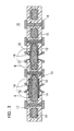
- Figs. 1 and 2 illustrate the structure of a first embodiment of the present invention.
- An aluminum sheet (Al sheet) 11, forming a metal core substrate of the printed circuit board, has a roughed surface. Specifically, micro-irregularities are formed on the surface of the foil-shaped aluminum sheet 11 by e.g., etching.
- a metal sheet e.g., aluminum sheet 11 as a core substrate, it is possible to reduce the substrate thickness and yet to provide for the required strength.
- an aluminum oxide (Al oxide) layer 12 as a dielectric film for a capacitor, is formed to a thickness having e.g., hundreds of picometers (pm), where 1 pm is 10 -12 m, as a lower limit and having e.g., tens of nanometers (nm) as an upper limit.
- the thin film of the aluminum oxide layer 12 may be formed by any suitable film-forming method, such as a sputtering method.
- an oxide film, formed by the aluminum oxide layer 12, having a high dielectric constant is formed on the aluminum sheet 11, having a surface area increased by the roughing processing, whereby the capacitance of the capacitor is increased by reduction in the capacitor thickness and the enlarged electrode surface area.
- a solid electrolyte layer such as a layer of an electrically conductive high molecular material (e.g., polymer) 13.
- the thin film of the aluminum oxide layer 12 is coated by a solid electrolyte material, such as by the layer of an electrically conductive high molecular material 13, to provide for insulating properties.
- the layer of the electrically conductive high molecular material 13 is formed of, for example, polypyrrole, which is a polymeric pyrrole layer or the like.
- an electrically conductive high molecular compound exhibiting electrical conductivity by doping a high molecular compound, having a conjugate system, such as polypyrrole, with a compound exhibiting electron donating or electron attracting properties, is used as a solid electrolyte material for a cathode.
- a layer of an electrically conductive chemical oxidation polymerization high molecular compound of polypyrrole, a graphite layer and a silver paste layer are formed on the surface of the dielectric oxide film in this order.
- the layer of an electrically conductive high molecular material 13 may be formed by e.g., polythiophene or polyaniline, etc. in place of polypyrrole.
- an electrically conductive paste 14 is formed as an electrically conductive electrode contact layer in a location of connection by a connection via (contact via) for the anode.
- This electrically conductive paste 14 is of a dual layer structure comprised of a silver paste layer deposited on a carbon paste layer.
- layers are encapsulated (sealed-in/sandwitched) by an insulating resin 15, such as epoxy resin.
- an insulating resin 15 such as epoxy resin.
- This printed circuit board 10 has the aluminum sheet 11 as an anode (+) and, with interposition of the aluminum oxide layer 12, has the electrically conductive paste 14 as a cathode (-). The electrical charges are accumulated in the spacing in-between.
- This printed circuit board 10 includes a through-hole 17 and a pair of copper plating sites 16, on both the front and back surfaces of the board, electrically connected to the through-hole 17, thus assuring signal interconnections across the front and back surfaces.
- the aluminum sheets 11A and 11B shown in the cross-sectional view of Fig. 1, are in unison (solid) with each other.
- the planar configuration of the aluminum sheets 11A and 11B may be of any desired optional pattern, such as annular or ⁇ pattern.
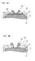
- Figs.2A and 2B are enlarged partial cross-sectional views showing an area A, shown encircled in Fig. 1 (a cathode connection via 18 and its vicinity), and an area B (an anode connection via 19 and its vicinity), respectively.
- the via for cathode connection includes an electrode 20, connected via electrically conductive paste 14 to the layer of the electrically conductive high molecular material 13, operating as a counter-electrode of the aluminum sheet 11.
- the aluminum oxide layer 12 is formed on the aluminum sheet 11, having the roughed surface, the layer of the electrically conductive high molecular material 13 is formed thereon, and the electrically conductive paste 14 is provided on the upper surface of the layer of the electrically conductive high molecular material 13.
- a hole (blind via) is bored in the encapsulating resin 15 by, for example is exposed laser irradiation, as deep as the electrically conductive paste 14 is exposed.
- the electrode 20 is formed by depositing an electrode material, such as copper, such as by plating.
- a hole (blind via) is bored in the resin 15, such as by laser irradiation, as deep as the surface of the aluminum sheet 11 is exposed, and an electrode material, such as copper, is deposited in the blind via by for example electroless plating to form the electrode 21.
- the electrode material such as copper
- the electrode material, such as copper is deposited conductor patterns (not shown) and in the inside of the through-hole 17 (see Fig. 1).
- the resin 15 surrounding the lateral sides of the electrode 21 has its bottom in abutting contact (intimate adhesion) with the aluminum sheet 11.
- the electrical insulation between the anode side electrode 21 and the cathode side layer of the electrically conductive high molecular material 13 around the via for anode side connection is assured by the resin 15 introduced into the space between the electrode 21 and the layer of the electrically conductive high molecular material 13 around the via for anode side connection.
- the capacitance of the capacitor may be increased, while the electrical insulation across the anode and the cathode may be secured by the resin 15.
- the surface roughness of the aluminum sheet 11 is e.g., 1 to 50 ⁇ m (micrometers), i.e., above the micrometer order, while the film thickness of the aluminum oxide layer 12 is, e.g., hundreds of pm (several Angstroms) to (several) tens of nm.
- the film thickness of the polypyrrole film forming the layer of the electrically conductive high molecular material 13 is e.g., 10 to 50 ⁇ m.
- the film thickness of the double-layer electrically conductive paste 14, composed of the carbon paste and the silver paste, is e.g., 5 to 20 ⁇ m, while the film thickness of the resin 15 is, e.g., 10 to 20 ⁇ m.
- the aluminum oxide layer 12 can be of an extremely reduced thickness, while the electrode surface area may be increased by the roughing processing of the aluminum sheet 11, while the polypyrrole film may be coated on the roughed surface of the aluminum sheet 11 with optimum follow-up characteristics, so that the counter-electrode of the aluminum sheet 11 can be increased in the surface area to realize a high capacitance.
- the capacitor of high capacitance may be realized, while the through-holes traversing the substrate are formed and a desired pattern is formed on the front and back surfaces of the substrate, so that the substrate may perform the role of an interposer.
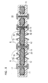
- an insulating resin 22 is formed in the via for anode side connection, around the site of connection to the aluminum sheet 11, to provide for electrical insulation across the electrode 21 on the anode side and the cathode side.
- Figs.4A and 4B are enlarged partial cross-sectional views showing an area A shown encircled in Fig.3 (a cathode connection via 18 and its vicinity) and an area B (an anode connection via 19 and its vicinity), to an enlarged scale, respectively.
- the structure of the second embodiment of the present invention differs from that of the above-described first embodiment only as to the via for anode side connection and is otherwise the same as the structure of the above-described first embodiment. That is, in the second embodiment of the present invention, the via for cathode side connection is similar in structure to that shown in Fig.2A. In the following, the via for anode side connection, by which the second embodiment differs from the above-described first embodiment, is explained.
- an aluminum board 11 there is formed no aluminum oxide layer nor a layer of an electrically conductive high molecular material in a via area for anode side connection, and a hole (blind via) is bored by, e.g., laser irradiation through the resin 15, until reaching the surface of the aluminum sheet 11, and an electrode material, such as copper, is deposited by for example electroless plating to form the electrode 21.
- An insulating resin 22 is deposited for laterally surrounding the bottom of the electrode 21 on the surface of the aluminum sheet 11 so that the insulating resin has its one surface in contact with the aluminum sheet 11.
- the opposite side surface of the insulating resin 22 has an elevated surface at a position vertically elevated from the aluminum sheet 11 flush with or higher in level than the layer of surface the electrically conductive high molecular material 13, and abuts against the resin 15 at the upper end of the insulating resin 22.
- the insulating resin 22 has its inner peripheral side surrounding a portion of the lateral side of the electrode 21, while having its outer peripheral surface abutting against the layer of the electrically conductive high molecular material 13 forming the counter-electrode.
- the electrical insulation across the electrode on the anode side 21 and the cathode side may be maintained in this manner by the insulating resin 22 provided on the aluminum sheet 11 between the electrode 21 and the electrically conductive high molecular material 13 on the aluminum sheet 11.
- the electrical insulation across the anode side electrode 21 and the layer of the electrically conductive high molecular material 13 is assured by the insulating resin 22.
- an etching resist operating as a mask for roughing processing of the aluminum sheet 11, may also be used, as will be explained later on in connection with the explanation of the manufacturing method.
- the etching resist in this case is left over unchanged on the aluminum sheet 11 after the roughing processing (the etching resist is termed a [permanent resist]).
- the area of the via for anode side connection on the surface of the aluminum sheet 11, and the near-by area where the insulating resin 22 is formed, are at a higher height level than the other peripheral area where there are provided the aluminum oxide layer 12 and the layer of the electrically conductive high molecular material 13, by way of providing a stepped structure.
- This stepped structure is afforded by etching the aluminum sheet 11, in the course of the surface roughing process of the aluminum sheet 11, using the insulating resin 22 as a mask.
- the height of the step difference of the aluminum sheet 11 and the thickness of the insulating resin 22 are set so that the lateral side of the insulating resin 22 will overlie the bottom surface and the upper surface of the layer of the electrically conductive high molecular material 13.
- the film thicknesses of the aluminum oxide layer 12 and the layer of the electrically conductive high molecular material 13 are selected to be similar to those of the first embodiment described above.
- the boring process of the via for anode side connection in the manufacture process for the printed circuit board is simplified.
- Fig.5 depicts the structure of the third embodiment of the present invention.
- the third embodiment of the present invention is similar to the second embodiment, explained with reference to Fig.3, except that the electrically conductive paste 14 is replaced by a metal plating layer 23. That is, in the present third embodiment, a layer of the electrically conductive high molecular material 13 of, for example, polypyrrole, is formed on the surface of the aluminum oxide layer 12, formed on the roughed surface of the aluminum sheet 11, the metal plating layer 23 is formed on the surface of the layer of the electrically conductive high molecular material 13, and a resin 15 is formed on the metal plating layer 23.
- the metal plating layer is formed of nickel, copper or indium.
- the via for anode side connection for assuring the contact with the aluminum sheet 11, has been removed on the metal plating layer 23.
- the insulating resin 22 is provided between the electrode 21 for the anode and the ends of the layer of the electrically conductive high molecular material 13 and the metal plating layer 23 for assuring electrical insulation.
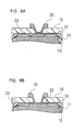
- Figs.6A and 6B are enlarged partial cross-sectional views showing an area A shown encircled in Fig.5 (a cathode connection via section 18 and its vicinity) and an area B (an anode connection via section 19 and its vicinity), respectively.
- Fig.5 a cathode connection via section 18 and its vicinity
- an area B an anode connection via section 19 and its vicinity
- the via section for cathode side connection includes an electrode 20 comprised of an electrically conducting member deposited in a via formed on boring the resin as far as the metal plating layer 23.
- the via section for anode side connection is not provided with the aluminum oxide layer 12 nor with the layer of the electrically conductive high molecular material 13.
- the metal plating layer 23 also is removed in an area of a via forming section for anode side connection.
- the via section for anode side connection is provided with an electrode 21 comprised of an electrically conducting member deposited in a via formed on boring the resin 15, such as by laser working, as far as the aluminum sheet 11.
- an insulating resin 22 having its one surface abutting against the aluminum sheet 11.
- the opposite side surface of the insulating resin 22 has an upstanding position from the surface of the aluminum sheet 11 flush with or at a higher height level than the metal plating layer 23 in the vicinity of the via for anode side connection, and is abutted against the resin 15.
- the insulating resin 22 has its inner peripheral surface surrounding a portion of the lateral surface of the electrode 21, while having its outer peripheral surface abutting against the ends of the metal plating layer 23 and the layer of the electrically conductive high molecular material 13.
- the electrical insulation between the electrode 21 of the anode and the cathode side by the insulating resin 22 provided between the electrode 21 on one hand and the metal plating layer 23 and the layer of the electrically conductive high molecular material 13 on the other hand is assured. That is, the electrical insulation between the anode electrode 21 on one hand and, the metal plating layer 23 and the layer of the electrically conductive high molecular material 13 on the other hand is assured by the insulating resin 22.
- an etching resist operating as a mask for roughing processing of the aluminum sheet 11, may also be used, as will be explained later on in connection with the explanation of the manufacturing method.
- the etching resist in this case is left over unchanged on the aluminum sheet 11 after the roughing processing.
- the area of the via for anode side connection on the surface of the aluminum sheet 11, and the near-by area where the insulating resin 22 is formed, is at a higher level than the other peripheral area where there are provided the aluminum oxide layer 12 and the layer of the electrically conductive high molecular material 13, by way of providing a stepped structure.
- This stepped structure is afforded by etching the aluminum sheet 11, in the course of the surface roughing process of the aluminum sheet 11, using the insulating resin 22 as a mask. It is noted that the film thicknesses of the aluminum oxide layer 12 and the layer of the electrically conductive high molecular material 13 are the same as those of the above-described first embodiment.
- FIG.7 depicts the structure of the fourth embodiment of the present invention.
- Fig.7 schematically shows the cross-section of a mounting structure in which a semiconductor device, such as CSP (chip size package), provided with the printed circuit board 10 of the aforementioned first embodiment, is mounted on a circuit substrate (motherboard) 130
- CSP chip size package
- the printed circuit board 10 operating as an interposer, includes the aluminum sheet 11, as a core substrate, an aluminum oxide layer 12 and a layer of the electrically conductive high molecular material 13.
- the printed circuit board 10 includes, in a contact via section on the cathode side, an electrically conductive paste and an electrode 20 deposited in the via reaching the electrically conductive paste.
- the printed circuit board 10 also includes, on an anode side contact via 19, an electrode 21 deposited in the via reaching the aluminum sheet 11, and a layer of an encapsulating resin 15.
- the printed circuit board 10 is provided with a plated through-hole 17.
- Bumps of LSI 110 are soldered by, for example a flip chip method, to electrode pads (land of a through-hole or a via pad) provided by the face-down system on one surface of the printed circuit board 10.
- Solder bumps 24 are provided in a grid configuration to the opposite side surface of the printed circuit board 10.
- a solder resist or a mold resist is charged into a space between the printed circuit board 10 and the LSI 110 to form a CSP semiconductor device of the flip chip ball grid array (BGA) type.
- BGA flip chip ball grid array
- the electrodes 20, 21 of the connection vias 18, 19 of the cathode and the anode on one surface of the printed circuit board 10 are connected to for example a power supply terminal 112 and to a grounding terminal (bump) 111, while the land of the through-hole 17 of the printed circuit board 10 is connected to a signal terminal (bump) 113 of the LSI 110.
- the BGA (ball grid array) of the CSP is soldered to the circuit substrate 130.
- electrode bumps 105 of the connection vias of the anode and the cathode are connected to a power supply pad and a ground pad of the circuit substrate (motherboard) 130.
- the semiconductor device, mounted on the circuit substrate 130, is sealed by an encapsulating resin 120.
- the electrodes 20, 21, as contact electrodes for the capacitor enclosed in the printed circuit board 10, are connected to a near-by terminal of the LSI 110.
- the capacitor may be applied to a capacitor as a decoupling capacitor and a noise filter in the high speed high frequency LSI 110.
- the semiconductor device, provided with the printed circuit board according to the instant invention as an interposer (package substrate) is not limited to the flip chip ball grid array (BGA) type semiconductor device.
- Fig.8 shows the structure of a fifth embodiment of the present invention.
- Fig.8 shows the structure in which the printed circuit board of the first embodiment shown in Fig. 1 is applied to a multi-layered printed circuit board.
- the fifth embodiment, shown in Fig.8, includes an aluminum sheet 11, as a core substrate, an aluminum oxide layer 12, as a dielectric film for a capacitor, and a layer of the electrically conductive high molecular material 13.
- the fifth embodiment also includes, in a contact via section on the cathode side, an electrically conductive paste 14, while including, on the cathode side contact via section 18, an electrode 20 reaching the electrically conductive paste 14.
- the anode side connection via 19 reaches the aluminum sheet 11 and is provided with an electrode 21.
- An interconnection layer (or layers) is(are) formed between the inter-layer insulating layers 15A and 15B and between the inter-layer insulating layers 15B and 15C.
- a cathode side connection via 18 and an anode side connection via 19 are provided as uppermost layers.
- An electrode 20A of the cathode side connection via 18A on the back surface is connected to the electrically conductive paste 14 of the uppermost layer via a pattern of the interconnection layer and the through-hole, while the electrode 21A of the anode side connection via 19A is connected to the aluminum sheet 11 as the uppermost layer via a pattern of the interconnection layer and the through-hole.
- Fig. 8 shows three-layered interconnections, it is not limitative of the present invention.
- FIG.9 to 11 schematically show the cross-section of the printed circuit board of the above-described first embodiment of the invention by way of illustrating the main manufacturing process step-by-step. It is noted that Figs.9 and 10 are split only for convenience in formulating the drawings.
- a hole is bored at a desired location in a foil-shaped aluminum sheet 11 by e.g., drilling to form a through-hole 9.
- the surface of the aluminum sheet 11 is etched for forming micro-irregularities therein.
- the surface roughness is on the order of e.g., 1 to 50 ⁇ m.
- an aluminum oxide layer 12 is formed as a dielectric film, as shown in Fig.9B, to a film thickness of e.g., hundreds of pm to tens of nm.
- the capacitance is increased by formation of an oxide film as a dielectric film on the aluminum surface the surface area of which has been increased by roughing.
- a polypyrrole film as a electrically conductive high molecular layer 13, then is formed on the aluminum oxide layer 12, to a film thickness of e.g., 10 to 50 ⁇ m, as shown in Fig.9C.
- the electrically conductive paste 14 is then formed in a location of the electrically conductive high molecular layer 13 (polypyrrole film) where the cathode contact via is to be formed, as shown in Fig. 10A.
- This electrically conductive paste is made up of two layers, namely a carbon paste layer and a silver paste layer.
- the film thickness of the electrically conductive paste 14 is e.g. 5 to 20 ⁇ m.
- boring for setting electrical connection to the aluminum sheet 11 is done by e.g., laser working, as shown in Fig. 10B.
- the layers of polypyrrole and aluminum oxide are then removed to expose the grounding surface of the aluminum sheet 11.
- a resin film is then bonded to each of the upper and lower surfaces, as shown in Fig. 11A, and the resin 15 is formed by vacuum laminating press.
- the film thickness of the resin 15 is set e.g., to 10 to 20 ⁇ m.
- a pre-hole 17a for the through-hole is formed, as shown in Fig. 11B.
- a pre-hole 18a for connection (contact) on the cathode side and a pre-hole 19a for connection (contact) on the anode side are also formed e.g., by laser working.
- the resin 15 is removed up to the upper surface of the electrically conductive paste 14 to expose the electrically conductive paste 14.
- the pre-hole 19a for connection on the anode side is formed by laser working until the aluminum sheet 11 is exposed. It is noted that the diameter of the pre-hole 19a for connection on the anode side is smaller than the diameter achieved in the boring step shown in Fig. 10B.
- the surface of the thermosetting insulating resin such as epoxy resin
- a catalyst is applied to the surface and into the inside of the via to provide catalyst followed by formation of a plating resist, not shown.
- the electroless plating is then carried out to precipitate copper (16 of Fig.1) to form a conductor pattern and a plating through-hole (17 of Fig. 1).
- the copper plating 16 is of a thickness of 5 to 25 ⁇ m.
- Figs.12 to 14 schematically show the cross-section of the printed circuit board of the above-described second embodiment of the invention by way of illustrating the main manufacturing process step-by-step. It is noted that Figs.12 to 14 are split only for convenience in formulating the drawings.
- a hole is bored at a desired location in a foil-shaped aluminum sheet 11 by e.g., drilling to form a through-hole.
- the insulating resin 22 is formed in a location of the surface of the aluminum sheet 11 where the contact to the aluminum sheet 11 is to be established, as shown in Fig.12B.
- the insulating resin (resist) 22 is formed prior to surface roughing of the aluminum sheet 11.
- an epoxy resin or a polyimide resin may be used.
- a modified photosensitive epoxy resin, or a photosensitive solder resist PSR4000 NAS-90-TY, manufactured by TAIYO INK SEIZO KK or DSR 2200 BGX-8, manufactured by TAMURA KAKEN, for example, may be used.
- the surface roughing processing for the aluminum sheet 11 is then carried out, using this insulating resin 22 as a mask.
- This roughing processing is by etching, as an example.
- the surface area of the aluminum sheet 11 other than its surface coated by the insulating resin 22 is roughed to form micro-irregularities.
- the surface of the aluminum sheet 11 coated with the insulating resin 22 is not roughed.
- the aluminum oxide layer 12 then is formed, as a dielectric film for a capacitor, so as to follow up with the micro-irregularities of the roughed surface of the aluminum sheet 11, as shown in Fig.12C.
- the film thickness of the aluminum oxide layer 12 is hundreds of pm to tens of nm. Since an oxide film forming a dielectric film has been formed on the aluminum sheet, the surface area of which has been enlarged by roughing processing, the capacitance value is increased.
- the aluminum oxide layer 12 is not formed on the surface area of the aluminum sheet 11 coated with the insulating resin 22.
- the polypyrrole film as a layer of the electrically conductive high molecular material (polymer) 13, is then formed on the aluminum oxide layer 12, as shown in Fig.13A.
- the film thickness of the polypyrrole film is 10 to 20 ⁇ m.
- the polypyrrole film is not formed on the surface area of the aluminum sheet 11 coated with the insulating resin 22. The lateral surface of the insulating resin 22 abuts against the end of the polypyrrole film 13.
- the electrically conductive paste 14 is then formed in a location of the layer of the electrically conductive high molecular material (polypyrrole film) 13 where the cathode contact via is to be formed, as shown in Fig. 13B.
- This electrically conductive paste is of a dual layer structure comprised of a carbon paste layer and a silver paste layer.
- a resin film then is bonded to each of the upper and lower surfaces, as shown in Fig.14A, to form the resin 15 by vacuum laminated press working.
- a pre-hole (basic hole)17a for a through-hole is then formed in a location of the resin 15 where the through-hole is to be formed.
- Pre-hole 18a for the cathode side connection (contact) and pre-hole 19a for connection on the anode side are then formed by for example laser working.
- the resin 15 is removed up to the upper surface of the electrically conductive paste 14 to expose the electrically conductive paste 14.
- a bore is formed in the resin 15 and in the insulating resin 22 to expose a portion of the surface of the site of the step difference of the aluminum sheet 11.
- the surface of the thermosetting insulating resin such as epoxy resin
- a catalyst(s) is applied to the surface and into the inside of the via to provide catalyst followed by formation of a plating resist, not shown.
- the electroless plating is then carried out to precipitate copper (16 of Fig.3) to form a conductor pattern and a through-hole (17 of Fig.3).
- the above process completes the printed circuit board shown in Fig.3.
- an additive method for example, is used. This technique is merely illustrative and is not intended to limit the present invention thereto, as described above.
- the insulating resin (resist) 22 as a mask for roughing processing, is formed in the surface area of the aluminum sheet 11 where the via for anode side connection 19 is to be formed. In the roughing processing, this surface area is not roughed, while neither the aluminum oxide layer 12 nor the layer of the electrically conductive high molecular material (polypyrrole film) 13 is formed.
- FIG. 13A A third embodiment of the manufacturing method for a printed circuit board according to the present invention, shown in Figs.5 and 6, is now explained.
- the metal plating layer 23 (see Figs.5 and 6) is formed in the process of Fig. 13B, in place of forming the electrically conductive paste layer.
- a pre-hole on the cathode side then is formed in the process step of Fig. 14B.
- the hole is bored by laser working until the metal plating layer 23 is exposed.
- a bore is formed in the resin 15 and in the subjacent insulating resin layer 22, with the laser working until the aluminum sheet 11 is exposed.
- the manufacturing process is otherwise the same as the manufacturing process for the printed circuit board of the first embodiment described above.
- the enclosed capacitor type printed circuit board can be produced, as the conventional process for manufacturing the printed circuit board is exploited, thereby reducing rise in the production cost to a minimum.
- a capacitor of a high capacitance value may be formed in the substrate without obstructing the laying of the interconnections of the printed circuit board.
- the electrode surface is roughed to increase its area, the oxide film having a high dielectric constant is formed to a reduced thickness, and the electrode-to-electrode distance is diminished to realize a printed circuit board having a capacitor of a large capacitance value enclosed therein.
- the electrical insulation across the anode electrode and the cathode electrode is maintained, such that a capacitor of a high capacitance value may be formed within the substrate, as the degree of freedom in designing is maintained, without inconvenience in laying the interconnections in the printed circuit board.
- the semiconductor device of the present invention it is possible to provide a package having enclosed therein a decoupling capacitor, a noise filter or a large capacitance capacitor array.
- a printed circuit board of the type having an enclosed capacitor can be produced, as the conventional manufacturing process for the printed circuit board is utilized, to render it possible to suppress the manufacturing cost of the printed circuit board of the type having an enclosed capacitor.
- the insulating member operating as a mask for roughing processing, is formed in an area in a metal sheet, in which to form the via for anode side connection. Since this area is not roughed, while neither the dielectric film for a capacitor nor a layer of an electrically conductive high molecular layer is formed in this area, the boring step needs to be carried out only once in forming the via for anode side connection, thereby simplifying the manufacture process for the printed circuit board of the type having an enclosed capacitor. It should be noted that other objects, features and aspects of the present invention will become apparent in the entire disclosure and that modifications may be done without departing the gist and scope of the present invention as disclosed herein and claimed as appended herewith. Also it should be noted that any combination of the disclosed and/or claimed elements, matters and/or items may fall under the modifications aforementioned.
Landscapes
- Engineering & Computer Science (AREA)
- Microelectronics & Electronic Packaging (AREA)
- Parts Printed On Printed Circuit Boards (AREA)
- Production Of Multi-Layered Print Wiring Board (AREA)
Applications Claiming Priority (2)
| Application Number | Priority Date | Filing Date | Title |
|---|---|---|---|
| JP2002185819A JP3711343B2 (ja) | 2002-06-26 | 2002-06-26 | 印刷配線板及びその製造方法並びに半導体装置 |
| JP2002185819 | 2002-06-26 |
Publications (3)
| Publication Number | Publication Date |
|---|---|
| EP1377141A2 true EP1377141A2 (de) | 2004-01-02 |
| EP1377141A3 EP1377141A3 (de) | 2005-10-19 |
| EP1377141B1 EP1377141B1 (de) | 2011-11-30 |
Family
ID=29717610
Family Applications (1)
| Application Number | Title | Priority Date | Filing Date |
|---|---|---|---|
| EP03014334A Expired - Lifetime EP1377141B1 (de) | 2002-06-26 | 2003-06-26 | Gedruckte Schaltungsplatte, Verfahren zu deren Herstellung und Halbleitervorrichtung |
Country Status (7)
| Country | Link |
|---|---|
| US (1) | US6882544B2 (de) |
| EP (1) | EP1377141B1 (de) |
| JP (1) | JP3711343B2 (de) |
| KR (1) | KR100534966B1 (de) |
| CN (1) | CN1258308C (de) |
| CA (1) | CA2433462C (de) |
| TW (1) | TWI224490B (de) |
Cited By (3)
| Publication number | Priority date | Publication date | Assignee | Title |
|---|---|---|---|---|
| US7317610B2 (en) * | 2004-11-16 | 2008-01-08 | Nec Toppan Circuit Solutions, Inc. | Sheet-shaped capacitor and method for manufacture thereof |
| EP2924406A4 (de) * | 2012-11-21 | 2016-07-13 | Sumitomo Riko Co Ltd | Lastsensor |
| CN114080104A (zh) * | 2020-08-19 | 2022-02-22 | 荣耀终端有限公司 | 电路板组件及电子设备 |
Families Citing this family (47)
| Publication number | Priority date | Publication date | Assignee | Title |
|---|---|---|---|---|
| US7065462B2 (en) * | 1998-07-24 | 2006-06-20 | Merilab, Inc. | Vehicle wheel alignment by rotating vision sensor |
| US7414858B2 (en) * | 2002-04-11 | 2008-08-19 | Koninklijke Philips Electronics N.V. | Method of manufacturing an electronic device |
| US7430128B2 (en) * | 2004-10-18 | 2008-09-30 | E.I. Du Pont De Nemours And Company | Capacitive/resistive devices, organic dielectric laminates and printed wiring boards incorporating such devices, and methods of making thereof |
| JP4599997B2 (ja) * | 2004-11-08 | 2010-12-15 | 凸版印刷株式会社 | 固体電解コンデンサを内蔵した配線基板の製造方法 |
| US20090302419A1 (en) * | 2004-11-26 | 2009-12-10 | Koninklijke Philips Electronics N.V. | Method of modifying surface area and electronic device |
| KR100656295B1 (ko) * | 2004-11-29 | 2006-12-11 | (주)웨이브닉스이에스피 | 선택적 양극 산화된 금속을 이용한 패키지 및 그 제작방법 |
| CN100544542C (zh) * | 2004-12-09 | 2009-09-23 | 鸿富锦精密工业(深圳)有限公司 | 防止静电放电的印刷电路板 |
| CN101010800B (zh) * | 2005-07-13 | 2012-02-01 | 松下电器产业株式会社 | 安装基板、安装体及使用安装基板和安装体的电子设备 |
| US7435627B2 (en) * | 2005-08-11 | 2008-10-14 | International Business Machines Corporation | Techniques for providing decoupling capacitance |
| US7361568B2 (en) * | 2005-12-21 | 2008-04-22 | Motorola, Inc. | Embedded capacitors and methods for their fabrication and connection |
| JP4839824B2 (ja) * | 2005-12-21 | 2011-12-21 | パナソニック株式会社 | コンデンサ内蔵基板およびその製造方法 |
| JP4731389B2 (ja) * | 2006-04-21 | 2011-07-20 | 佐賀三洋工業株式会社 | 積層型固体電解コンデンサ及びその製造方法 |
| US7605048B2 (en) * | 2007-04-06 | 2009-10-20 | Kemet Electronics Corporation | Method for forming a capacitor having a copper electrode and a high surface area aluminum inner layer |
| US7589394B2 (en) * | 2007-04-10 | 2009-09-15 | Ibiden Co., Ltd. | Interposer |
| KR100866577B1 (ko) * | 2007-09-28 | 2008-11-03 | 삼성전기주식회사 | 인쇄회로기판의 층간 도통방법 |
| TWI373118B (en) * | 2007-12-21 | 2012-09-21 | Ind Tech Res Inst | Through hole capacitor and method of manufacturing the same |
| CN101528008B (zh) * | 2008-03-03 | 2012-05-23 | 欣兴电子股份有限公司 | 线路板及其制造方法 |
| JP4525786B2 (ja) * | 2008-03-31 | 2010-08-18 | Tdk株式会社 | 電子部品及び電子部品モジュール |
| FI123205B (fi) * | 2008-05-12 | 2012-12-31 | Imbera Electronics Oy | Piirimoduuli ja menetelmä piirimoduulin valmistamiseksi |
| CN101594740B (zh) * | 2008-05-27 | 2012-06-06 | 华通电脑股份有限公司 | 嵌埋电子器件的电路板及其方法 |
| KR100967103B1 (ko) | 2008-06-30 | 2010-07-05 | 주식회사 하이닉스반도체 | 클럭생성회로 및 클럭생성방법 |
| KR101628355B1 (ko) * | 2008-10-30 | 2016-06-21 | 엘지이노텍 주식회사 | 임베디드 커패시터 및 그 제조방법 |
| DE102008061928A1 (de) * | 2008-12-15 | 2010-06-17 | Polylc Gmbh & Co. Kg | Organisch elektronische Schaltung |
| KR101204187B1 (ko) * | 2010-11-02 | 2012-11-23 | 삼성전기주식회사 | 소성 접합을 이용한 파워 모듈 및 그 제조 방법 |
| US9013893B2 (en) | 2010-12-29 | 2015-04-21 | Industrial Technology Research Institute | Embedded capacitor module |
| TWI405322B (zh) | 2010-12-29 | 2013-08-11 | 財團法人工業技術研究院 | 內藏電容基板模組 |
| TWI483352B (zh) * | 2012-03-12 | 2015-05-01 | Ind Tech Res Inst | 固態電解電容基板模組及包括該固態電解電容基板模組的電路板 |
| JP2014086651A (ja) * | 2012-10-26 | 2014-05-12 | Ibiden Co Ltd | プリント配線板及びプリント配線板の製造方法 |
| DE102013005486B4 (de) * | 2013-04-02 | 2019-02-14 | Heraeus Deutschland GmbH & Co. KG | Schichtstruktur mit leitfähigem Polymer zur Manipulationserkennung sowie Verfahren zu deren Herstellung |
| CN104185365B (zh) * | 2013-05-23 | 2018-06-26 | 比亚迪股份有限公司 | 一种线路板及其制备方法 |
| CN104349592B (zh) * | 2013-08-09 | 2017-08-25 | 鹏鼎控股(深圳)股份有限公司 | 多层电路板及其制作方法 |
| CN103708412B (zh) * | 2013-10-29 | 2016-01-20 | 太原科技大学 | 一种微机电系统封装方法 |
| JP2015095587A (ja) * | 2013-11-13 | 2015-05-18 | 日本特殊陶業株式会社 | 多層配線基板 |
| TWI554174B (zh) * | 2014-11-04 | 2016-10-11 | 上海兆芯集成電路有限公司 | 線路基板和半導體封裝結構 |
| JP2017162913A (ja) * | 2016-03-08 | 2017-09-14 | イビデン株式会社 | 配線板及びその製造方法 |
| CN107665879A (zh) * | 2016-07-29 | 2018-02-06 | 奥特斯奥地利科技与系统技术有限公司 | 器件载体及包括所述器件载体的电子系统 |
| US10361149B2 (en) * | 2016-08-10 | 2019-07-23 | Qualcomm Incorporated | Land grid array (LGA) packaging of passive-on-glass (POG) structure |
| JP2019021879A (ja) * | 2017-07-21 | 2019-02-07 | 日本特殊陶業株式会社 | 配線基板及びプレーナトランス |
| KR102154313B1 (ko) * | 2017-08-24 | 2020-09-09 | 동우 화인켐 주식회사 | 필름 안테나 및 이를 포함하는 디스플레이 장치 |
| JP6719687B1 (ja) * | 2019-08-30 | 2020-07-08 | 三菱電機株式会社 | 半導体装置 |
| CA3170472A1 (en) * | 2020-02-06 | 2021-08-12 | Venkatesh Sundaram | Planar high-density aluminum capacitors for stacking and embedding |
| CN111653542A (zh) * | 2020-06-17 | 2020-09-11 | 佛山市蓝箭电子股份有限公司 | 一种半导体封装引线框架 |
| CN115917685B (zh) * | 2021-04-30 | 2025-04-08 | 株式会社村田制作所 | 集成型电容器以及集成型电容器的制造方法 |
| US20240290705A1 (en) * | 2023-02-28 | 2024-08-29 | Lux Semiconductors, Inc. | Metal core substrate based package interconnect systems |
| TWI898543B (zh) * | 2023-06-16 | 2025-09-21 | 日商村田製作所股份有限公司 | 電容器元件 |
| CN119545658A (zh) * | 2023-08-30 | 2025-02-28 | 宏启胜精密电子(秦皇岛)有限公司 | 电路板和其制造方法 |
| US12538427B2 (en) | 2023-09-26 | 2026-01-27 | Garuda Technology Co., Ltd. | Circuit board and method of manufacturing the same |
Citations (6)
| Publication number | Priority date | Publication date | Assignee | Title |
|---|---|---|---|---|
| JPH0794368A (ja) | 1993-07-27 | 1995-04-07 | Nec Corp | 固体電解コンデンサおよびその製造方法 |
| JP2738590B2 (ja) | 1989-08-23 | 1998-04-08 | ザイコン コーポレーション | 印刷配線基板のためのコンデンサ積層体 |
| DE19847946A1 (de) | 1998-10-09 | 2000-04-27 | Siemens Ag | Mehrlagen-Leiterplatte mit integriertem Kondensator |
| EP1154480A2 (de) | 2000-05-08 | 2001-11-14 | Shinko Electric Industries Co. Ltd. | Verbindungsplatte und Halbleiter damit |
| EP1202300A2 (de) | 2000-10-12 | 2002-05-02 | Matsushita Electric Industrial Co., Ltd. | Elektrolytkondensator, Schaltungsplatte mit diesem Elektrolytkondensator, und dessen Herstellungsverfahren |
| US20020054471A1 (en) | 2000-08-30 | 2002-05-09 | International Business Machines Corporation | Method of making a parallel capacitor laminate |
Family Cites Families (4)
| Publication number | Priority date | Publication date | Assignee | Title |
|---|---|---|---|---|
| US5745984A (en) * | 1995-07-10 | 1998-05-05 | Martin Marietta Corporation | Method for making an electronic module |
| CN100381027C (zh) * | 1999-09-02 | 2008-04-09 | 伊比登株式会社 | 印刷布线板及其制造方法 |
| JP4717268B2 (ja) * | 2001-01-12 | 2011-07-06 | 富士通株式会社 | 絶縁樹脂組成物及びそれから形成した絶縁層を含む多層回路基板 |
| KR100891269B1 (ko) * | 2001-01-31 | 2009-04-06 | 소니 가부시끼 가이샤 | 반도체 장치 및 그 제조 방법 |
-
2002
- 2002-06-26 JP JP2002185819A patent/JP3711343B2/ja not_active Expired - Fee Related
-
2003
- 2003-06-24 KR KR10-2003-0041036A patent/KR100534966B1/ko not_active Expired - Fee Related
- 2003-06-24 CN CNB031477771A patent/CN1258308C/zh not_active Expired - Fee Related
- 2003-06-25 US US10/602,828 patent/US6882544B2/en not_active Expired - Fee Related
- 2003-06-25 CA CA002433462A patent/CA2433462C/en not_active Expired - Fee Related
- 2003-06-26 EP EP03014334A patent/EP1377141B1/de not_active Expired - Lifetime
- 2003-06-26 TW TW092117421A patent/TWI224490B/zh not_active IP Right Cessation
Patent Citations (7)
| Publication number | Priority date | Publication date | Assignee | Title |
|---|---|---|---|---|
| JP2738590B2 (ja) | 1989-08-23 | 1998-04-08 | ザイコン コーポレーション | 印刷配線基板のためのコンデンサ積層体 |
| JPH0794368A (ja) | 1993-07-27 | 1995-04-07 | Nec Corp | 固体電解コンデンサおよびその製造方法 |
| DE19847946A1 (de) | 1998-10-09 | 2000-04-27 | Siemens Ag | Mehrlagen-Leiterplatte mit integriertem Kondensator |
| EP1154480A2 (de) | 2000-05-08 | 2001-11-14 | Shinko Electric Industries Co. Ltd. | Verbindungsplatte und Halbleiter damit |
| JP2001320171A (ja) | 2000-05-08 | 2001-11-16 | Shinko Electric Ind Co Ltd | 多層配線基板及び半導体装置 |
| US20020054471A1 (en) | 2000-08-30 | 2002-05-09 | International Business Machines Corporation | Method of making a parallel capacitor laminate |
| EP1202300A2 (de) | 2000-10-12 | 2002-05-02 | Matsushita Electric Industrial Co., Ltd. | Elektrolytkondensator, Schaltungsplatte mit diesem Elektrolytkondensator, und dessen Herstellungsverfahren |
Cited By (4)
| Publication number | Priority date | Publication date | Assignee | Title |
|---|---|---|---|---|
| US7317610B2 (en) * | 2004-11-16 | 2008-01-08 | Nec Toppan Circuit Solutions, Inc. | Sheet-shaped capacitor and method for manufacture thereof |
| EP2924406A4 (de) * | 2012-11-21 | 2016-07-13 | Sumitomo Riko Co Ltd | Lastsensor |
| CN114080104A (zh) * | 2020-08-19 | 2022-02-22 | 荣耀终端有限公司 | 电路板组件及电子设备 |
| CN114080104B (zh) * | 2020-08-19 | 2022-09-27 | 荣耀终端有限公司 | 电路板组件及电子设备 |
Also Published As
| Publication number | Publication date |
|---|---|
| JP3711343B2 (ja) | 2005-11-02 |
| EP1377141A3 (de) | 2005-10-19 |
| US20040246690A1 (en) | 2004-12-09 |
| CN1471353A (zh) | 2004-01-28 |
| KR20040002664A (ko) | 2004-01-07 |
| EP1377141B1 (de) | 2011-11-30 |
| JP2004031641A (ja) | 2004-01-29 |
| TW200405785A (en) | 2004-04-01 |
| US6882544B2 (en) | 2005-04-19 |
| CA2433462C (en) | 2006-09-12 |
| CA2433462A1 (en) | 2003-12-26 |
| TWI224490B (en) | 2004-11-21 |
| KR100534966B1 (ko) | 2005-12-08 |
| CN1258308C (zh) | 2006-05-31 |
Similar Documents
| Publication | Publication Date | Title |
|---|---|---|
| US6882544B2 (en) | Printed circuit board, method for producing same and semiconductor device | |
| US7317610B2 (en) | Sheet-shaped capacitor and method for manufacture thereof | |
| US7889509B2 (en) | Ceramic capacitor | |
| US6930257B1 (en) | Integrated circuit substrate having laminated laser-embedded circuit layers | |
| US7230818B2 (en) | Printed circuit board and manufacturing method thereof | |
| US7745924B2 (en) | Capacitor embedded in interposer, semiconductor device including the same, and method for manufacturing capacitor embedded in interposer | |
| WO2006082838A1 (ja) | 多層配線基板とその製造方法、および多層配線基板を用いた半導体装置と電子機器 | |
| WO2002054421A2 (en) | Multiple tier array capacitor and methods of fabrication therefor | |
| KR20030088357A (ko) | 금속 코어 기판 및 그 제조 방법 | |
| TW200305260A (en) | Multi-layered semiconductor device and method of manufacturing same | |
| WO2004112135A1 (ja) | 半導体装置用基板および半導体装置 | |
| JP5020671B2 (ja) | コンデンサ内蔵配線基板 | |
| JP2000151112A (ja) | 配線基板及びその製造方法 | |
| JP2006147607A (ja) | 印刷配線板及びその製造方法並びに半導体装置 | |
| CN101038886A (zh) | 内埋元件的基板制造方法 | |
| TW200919676A (en) | Packaging substrate structure having capacitor embedded therein and method for manufacturing the same | |
| HK1061952A (en) | Printed circuit board, method for producing same and semiconductor device | |
| JP4814129B2 (ja) | 部品内蔵配線基板、配線基板内蔵用部品 | |
| JP3945764B2 (ja) | 配線基板 | |
| JP5122846B2 (ja) | コンデンサ内蔵配線基板 | |
| JP4795860B2 (ja) | コンデンサ、配線基板 | |
| JP5913535B1 (ja) | 部品内蔵基板及びその製造方法 | |
| TWI224389B (en) | Semiconductor package substrate with embedded resistors and method for fabricating the same | |
| TW200931456A (en) | Packaging substrate having capacitor embedded therein and method for manufacturing the same | |
| CN101038881A (zh) | 一种基板的制造方法 |
Legal Events
| Date | Code | Title | Description |
|---|---|---|---|
| PUAI | Public reference made under article 153(3) epc to a published international application that has entered the european phase |
Free format text: ORIGINAL CODE: 0009012 |
|
| AK | Designated contracting states |
Kind code of ref document: A2 Designated state(s): AT BE BG CH CY CZ DE DK EE ES FI FR GB GR HU IE IT LI LU MC NL PT RO SE SI SK TR |
|
| AX | Request for extension of the european patent |
Extension state: AL LT LV MK |
|
| REG | Reference to a national code |
Ref country code: HK Ref legal event code: DE Ref document number: 1061952 Country of ref document: HK |
|
| PUAL | Search report despatched |
Free format text: ORIGINAL CODE: 0009013 |
|
| AK | Designated contracting states |
Kind code of ref document: A3 Designated state(s): AT BE BG CH CY CZ DE DK EE ES FI FR GB GR HU IE IT LI LU MC NL PT RO SE SI SK TR |
|
| AX | Request for extension of the european patent |
Extension state: AL LT LV MK |
|
| RAP1 | Party data changed (applicant data changed or rights of an application transferred) |
Owner name: NEC TOPPAN CIRCUIT SOLUTIONS, INC. Owner name: NEC TOKIN CORPORATION |
|
| 17P | Request for examination filed |
Effective date: 20060203 |
|
| AKX | Designation fees paid |
Designated state(s): DE FR GB IT |
|
| 17Q | First examination report despatched |
Effective date: 20090710 |
|
| GRAP | Despatch of communication of intention to grant a patent |
Free format text: ORIGINAL CODE: EPIDOSNIGR1 |
|
| GRAS | Grant fee paid |
Free format text: ORIGINAL CODE: EPIDOSNIGR3 |
|
| GRAA | (expected) grant |
Free format text: ORIGINAL CODE: 0009210 |
|
| AK | Designated contracting states |
Kind code of ref document: B1 Designated state(s): DE FR GB IT |
|
| REG | Reference to a national code |
Ref country code: GB Ref legal event code: FG4D |
|
| REG | Reference to a national code |
Ref country code: DE Ref legal event code: R096 Ref document number: 60339246 Country of ref document: DE Effective date: 20120301 |
|
| PGFP | Annual fee paid to national office [announced via postgrant information from national office to epo] |
Ref country code: DE Payment date: 20120616 Year of fee payment: 10 |
|
| PG25 | Lapsed in a contracting state [announced via postgrant information from national office to epo] |
Ref country code: IT Free format text: LAPSE BECAUSE OF FAILURE TO SUBMIT A TRANSLATION OF THE DESCRIPTION OR TO PAY THE FEE WITHIN THE PRESCRIBED TIME-LIMIT Effective date: 20111130 |
|
| PGFP | Annual fee paid to national office [announced via postgrant information from national office to epo] |
Ref country code: GB Payment date: 20120612 Year of fee payment: 10 |
|
| PLBE | No opposition filed within time limit |
Free format text: ORIGINAL CODE: 0009261 |
|
| STAA | Information on the status of an ep patent application or granted ep patent |
Free format text: STATUS: NO OPPOSITION FILED WITHIN TIME LIMIT |
|
| 26N | No opposition filed |
Effective date: 20120831 |
|
| REG | Reference to a national code |
Ref country code: DE Ref legal event code: R097 Ref document number: 60339246 Country of ref document: DE Effective date: 20120831 |
|
| REG | Reference to a national code |
Ref country code: HK Ref legal event code: WD Ref document number: 1061952 Country of ref document: HK |
|
| REG | Reference to a national code |
Ref country code: FR Ref legal event code: ST Effective date: 20130228 |
|
| PG25 | Lapsed in a contracting state [announced via postgrant information from national office to epo] |
Ref country code: FR Free format text: LAPSE BECAUSE OF NON-PAYMENT OF DUE FEES Effective date: 20120702 |
|
| GBPC | Gb: european patent ceased through non-payment of renewal fee |
Effective date: 20130626 |
|
| REG | Reference to a national code |
Ref country code: DE Ref legal event code: R119 Ref document number: 60339246 Country of ref document: DE Effective date: 20140101 |
|
| PG25 | Lapsed in a contracting state [announced via postgrant information from national office to epo] |
Ref country code: DE Free format text: LAPSE BECAUSE OF NON-PAYMENT OF DUE FEES Effective date: 20140101 Ref country code: GB Free format text: LAPSE BECAUSE OF NON-PAYMENT OF DUE FEES Effective date: 20130626 |