EP1378009B1 - Structure de transistor a effet de champ et son procede de production - Google Patents
Structure de transistor a effet de champ et son procede de production Download PDFInfo
- Publication number
- EP1378009B1 EP1378009B1 EP02708575A EP02708575A EP1378009B1 EP 1378009 B1 EP1378009 B1 EP 1378009B1 EP 02708575 A EP02708575 A EP 02708575A EP 02708575 A EP02708575 A EP 02708575A EP 1378009 B1 EP1378009 B1 EP 1378009B1
- Authority
- EP
- European Patent Office
- Prior art keywords
- region
- gate
- layer
- field plate
- source
- Prior art date
- Legal status (The legal status is an assumption and is not a legal conclusion. Google has not performed a legal analysis and makes no representation as to the accuracy of the status listed.)
- Expired - Lifetime
Links
Images




Classifications
-
- H—ELECTRICITY
- H10—SEMICONDUCTOR DEVICES; ELECTRIC SOLID-STATE DEVICES NOT OTHERWISE PROVIDED FOR
- H10D—INORGANIC ELECTRIC SEMICONDUCTOR DEVICES
- H10D30/00—Field-effect transistors [FET]
- H10D30/60—Insulated-gate field-effect transistors [IGFET]
-
- H—ELECTRICITY
- H10—SEMICONDUCTOR DEVICES; ELECTRIC SOLID-STATE DEVICES NOT OTHERWISE PROVIDED FOR
- H10D—INORGANIC ELECTRIC SEMICONDUCTOR DEVICES
- H10D64/00—Electrodes of devices having potential barriers
- H10D64/111—Field plates
- H10D64/112—Field plates comprising multiple field plate segments
-
- H—ELECTRICITY
- H10—SEMICONDUCTOR DEVICES; ELECTRIC SOLID-STATE DEVICES NOT OTHERWISE PROVIDED FOR
- H10D—INORGANIC ELECTRIC SEMICONDUCTOR DEVICES
- H10D30/00—Field-effect transistors [FET]
- H10D30/01—Manufacture or treatment
- H10D30/021—Manufacture or treatment of FETs having insulated gates [IGFET]
- H10D30/028—Manufacture or treatment of FETs having insulated gates [IGFET] of double-diffused metal oxide semiconductor [DMOS] FETs
- H10D30/0281—Manufacture or treatment of FETs having insulated gates [IGFET] of double-diffused metal oxide semiconductor [DMOS] FETs of lateral DMOS [LDMOS] FETs
-
- H—ELECTRICITY
- H10—SEMICONDUCTOR DEVICES; ELECTRIC SOLID-STATE DEVICES NOT OTHERWISE PROVIDED FOR
- H10D—INORGANIC ELECTRIC SEMICONDUCTOR DEVICES
- H10D30/00—Field-effect transistors [FET]
- H10D30/60—Insulated-gate field-effect transistors [IGFET]
- H10D30/64—Double-diffused metal-oxide semiconductor [DMOS] FETs
- H10D30/65—Lateral DMOS [LDMOS] FETs
- H10D30/657—Lateral DMOS [LDMOS] FETs having substrates comprising insulating layers, e.g. SOI-LDMOS transistors
-
- H—ELECTRICITY
- H10—SEMICONDUCTOR DEVICES; ELECTRIC SOLID-STATE DEVICES NOT OTHERWISE PROVIDED FOR
- H10D—INORGANIC ELECTRIC SEMICONDUCTOR DEVICES
- H10D64/00—Electrodes of devices having potential barriers
- H10D64/111—Field plates
-
- H—ELECTRICITY
- H10—SEMICONDUCTOR DEVICES; ELECTRIC SOLID-STATE DEVICES NOT OTHERWISE PROVIDED FOR
- H10D—INORGANIC ELECTRIC SEMICONDUCTOR DEVICES
- H10D64/00—Electrodes of devices having potential barriers
- H10D64/60—Electrodes characterised by their materials
- H10D64/66—Electrodes having a conductor capacitively coupled to a semiconductor by an insulator, e.g. MIS electrodes
- H10D64/671—Electrodes having a conductor capacitively coupled to a semiconductor by an insulator, e.g. MIS electrodes the conductor having lateral variation in doping or structure
-
- H—ELECTRICITY
- H10—SEMICONDUCTOR DEVICES; ELECTRIC SOLID-STATE DEVICES NOT OTHERWISE PROVIDED FOR
- H10D—INORGANIC ELECTRIC SEMICONDUCTOR DEVICES
- H10D84/00—Integrated devices formed in or on semiconductor substrates that comprise only semiconducting layers, e.g. on Si wafers or on GaAs-on-Si wafers
- H10D84/101—Integrated devices comprising main components and built-in components, e.g. IGBT having built-in freewheel diode
- H10D84/151—LDMOS having built-in components
- H10D84/158—LDMOS having built-in components the built-in components being breakdown diodes, e.g. Zener diodes
-
- H—ELECTRICITY
- H10—SEMICONDUCTOR DEVICES; ELECTRIC SOLID-STATE DEVICES NOT OTHERWISE PROVIDED FOR
- H10D—INORGANIC ELECTRIC SEMICONDUCTOR DEVICES
- H10D62/00—Semiconductor bodies, or regions thereof, of devices having potential barriers
- H10D62/10—Shapes, relative sizes or dispositions of the regions of the semiconductor bodies; Shapes of the semiconductor bodies
- H10D62/13—Semiconductor regions connected to electrodes carrying current to be rectified, amplified or switched, e.g. source or drain regions
- H10D62/149—Source or drain regions of field-effect devices
- H10D62/151—Source or drain regions of field-effect devices of IGFETs
-
- H—ELECTRICITY
- H10—SEMICONDUCTOR DEVICES; ELECTRIC SOLID-STATE DEVICES NOT OTHERWISE PROVIDED FOR
- H10D—INORGANIC ELECTRIC SEMICONDUCTOR DEVICES
- H10D62/00—Semiconductor bodies, or regions thereof, of devices having potential barriers
- H10D62/10—Shapes, relative sizes or dispositions of the regions of the semiconductor bodies; Shapes of the semiconductor bodies
- H10D62/13—Semiconductor regions connected to electrodes carrying current to be rectified, amplified or switched, e.g. source or drain regions
- H10D62/149—Source or drain regions of field-effect devices
- H10D62/151—Source or drain regions of field-effect devices of IGFETs
- H10D62/156—Drain regions of DMOS transistors
- H10D62/157—Impurity concentrations or distributions
-
- H—ELECTRICITY
- H10—SEMICONDUCTOR DEVICES; ELECTRIC SOLID-STATE DEVICES NOT OTHERWISE PROVIDED FOR
- H10D—INORGANIC ELECTRIC SEMICONDUCTOR DEVICES
- H10D64/00—Electrodes of devices having potential barriers
- H10D64/20—Electrodes characterised by their shapes, relative sizes or dispositions
- H10D64/27—Electrodes not carrying the current to be rectified, amplified, oscillated or switched, e.g. gates
- H10D64/311—Gate electrodes for field-effect devices
- H10D64/411—Gate electrodes for field-effect devices for FETs
- H10D64/511—Gate electrodes for field-effect devices for FETs for IGFETs
- H10D64/514—Gate electrodes for field-effect devices for FETs for IGFETs characterised by the insulating layers
- H10D64/516—Gate electrodes for field-effect devices for FETs for IGFETs characterised by the insulating layers the thicknesses being non-uniform
-
- H—ELECTRICITY
- H10—SEMICONDUCTOR DEVICES; ELECTRIC SOLID-STATE DEVICES NOT OTHERWISE PROVIDED FOR
- H10D—INORGANIC ELECTRIC SEMICONDUCTOR DEVICES
- H10D89/00—Aspects of integrated devices not covered by groups H10D84/00 - H10D88/00
- H10D89/60—Integrated devices comprising arrangements for electrical or thermal protection, e.g. protection circuits against electrostatic discharge [ESD]
- H10D89/601—Integrated devices comprising arrangements for electrical or thermal protection, e.g. protection circuits against electrostatic discharge [ESD] for devices having insulated gate electrodes, e.g. for IGFETs or IGBTs
- H10D89/611—Integrated devices comprising arrangements for electrical or thermal protection, e.g. protection circuits against electrostatic discharge [ESD] for devices having insulated gate electrodes, e.g. for IGFETs or IGBTs using diodes as protective elements
-
- H—ELECTRICITY
- H10—SEMICONDUCTOR DEVICES; ELECTRIC SOLID-STATE DEVICES NOT OTHERWISE PROVIDED FOR
- H10P—GENERIC PROCESSES OR APPARATUS FOR THE MANUFACTURE OR TREATMENT OF DEVICES COVERED BY CLASS H10
- H10P30/00—Ion implantation into wafers, substrates or parts of devices
- H10P30/20—Ion implantation into wafers, substrates or parts of devices into semiconductor materials, e.g. for doping
- H10P30/22—Ion implantation into wafers, substrates or parts of devices into semiconductor materials, e.g. for doping using masks
Definitions
- the invention relates to an insulated gate field effect transistor structure and further to a method of manufacturing such a structure.
- IGFET insulated gate field effect transistor
- MOS Metal Oxide Semiconductor
- a double diffused MOS (DMOS) structure may be used in which a long lateral path, known as the drift region, extends between drain and source diffusions.
- the drift region attenuates any high voltages applied between drain and source down to around 20V in the channel region controlled by the gate.
- the drift region In order to maximise the voltage capability of the transistor, the drift region would ideally be long and or lightly doped. Unfortunately, these properties would mean that the drift region would contribute a relatively high resistance to the overall device when the transistor is on. To address this, it is known to dope the drift region with an appropriate doping profile and to choose its thickness such that the reversed bias junctions between the MOSFET channel and source and between the channel and the substrate deplete the entire drift region of charge carriers when the device is turned off. This creates a uniform electric field in the drift region when a large voltage is applied across the transistor when switched off, which maximises the breakdown voltage since there are no peaks in the electric field to initiate premature avalanche breakdown. The fully depleted drift region is said to be in a RESURF (reduced surface field) condition. In a RESURF structure, the full thickness of the drift region is depleted when the device is turned off.
- RESURF reduced surface field
- the device is a silicon on insulator (SOI) device having a layer of silicon 101 formed on a buried oxide layer 103 on a semiconductor substrate 105. Source 107 and drain 109 regions are formed in the silicon, and connected to source 108 and drain 110 contacts respectively.
- SOI silicon on insulator
- a gate layer 111 is provided over part of the silicon layer 101 which forms a channel, separated from the channel by a gate oxide 112.
- the gate layer is connected to a gate contact 113.
- the gate controls conduction between source 107 and drain 109, as is well known.
- drift region 119 is provided in the silicon layer 101 to allow large voltages (e.g. 100V or more) to be applied between source and drain.
- large voltages e.g. 100V or more
- a large voltage applied across source and drain may be at least partially dropped in the drift region thus reducing the voltage dropped in the channel.
- a field plate 115 is formed integrally with the gate layer 111 over the LOCOS oxide layer 114 and extends laterally over the drift region 119 in the silicon layer 101. When the device is turned off, the field plate depletes the drift region to provide a RESURF effect.
- the drift region 119 is protected from the effects of an impinging electric field, such as may be caused by moisture or other charged contaminants on the surface of the wafer, by the field plate 115. Electric fields will terminate on the field plate 115.
- the drift region 119 may be depleted from the top which means that the device can be designed with a higher doping level in the drift region than would otherwise be possible. This means that the device of US-A-5,412,241 can be made with a low on-resistance.
- Such silicon on insulator device structures exhibit, by virtue of their structure, low values of the capacitance between gate and drain (C gd ) and the charge needed to be supplied through gate and drain to switch the device (Q gd ). These low values of C gd and Q gd give rise to rapid switching, i.e. a rapid response to changes in gate voltage.
- IGFET devices are highly sensitive to excessive voltages. If too high a voltage is present between the gate and the channel the gate insulator may break down and destroy the device. Such high voltages may simply be present in the circuit in which the IGFET device is mounted or alternatively the voltage may be electrostatic. It is accordingly highly beneficial to provide suitable protection for the gate, known as electrostatic discharge protection.
- a field effect transistor structure comprising: a source region and a drain region laterally spaced in a semiconductor body layer; a channel and a drift region in the semiconductor body layer between the source region and the drain region; an oxide layer over the channel and the drift region; an upper semiconductor layer arranged over the oxide layer, the upper semiconductor layer being doped to have a gate region arranged over the channel, a field plate region arranged over the drift region and at least one p-n junction forming at least one diode between the field plate region and the gate region; wherein an electrical interconnection is provided between the source region and the field plate region to electrically connect the source region and the field plate region.
- the transistor structure thus provides at least one electrostatic protection diode in a simple structure that is convenient to manufacture.
- the diode or diodes provided in the structure according to the invention protect the gate from electrostatic discharge by virtue of Zener action. If too high a voltage is present between gate and source, the diode or diodes undergo reverse breakdown to allow current to flow between gate and source.
- the source-connected field plate region acts as a Faraday screen between gate and drain so reducing C gd and hence the charge needed to be applied through gate and drain. This decreases the switching time.
- the gate-connected field plate of US-A-5,412,241 allows the drift region to be depleted by a suitable voltage on the gate and hence on the field plate.
- This prior art arrangement will normally increase C gd rather than reduce it as in the present invention. Accordingly, the prior art arrangement will tend to increase switching time.
- the transistor structure is preferably formed to have source and drain regions of a first conductivity type.
- the drift region may be of the same conductivity type but of lower doping, and the channel may be formed in a body region of opposite conductivity type.
- the first conductivity type may be n-type.
- the p and n regions of the upper semiconductor layer preferably alternate to form at least one diode.
- At least one pair of back to back diodes may be provided in the upper semiconductor layer between the gate region and the field plate region.
- a plurality of back to back diodes may be provided to increase the maximum voltage between source and gate before breakdown occurs.
- the upper semiconductor layer including the gate region and the field plate region may be fabricated from any convenient semiconducting material, such as polysilicon.
- the field plate region may be doped n+ or p+.
- the drift region may be linearly graded, i.e. it may have a concentration of dopant that varies linearly, decreasing away from the drain region. This may result in an improved breakdown performance compared with a drift region of constant concentration.
- the invention may be implemented in a SOI structure, with a substrate, a buried oxide layer on the substrate and the semiconductor body layer deposited on the buried oxide layer. Source, drain, channel and drift regions may be formed from implantations in the deposited semiconductor body layer.
- SOI structures offer advantages, such as intrinsically lower capacitance.
- the oxide layer may include a LOCOS layer above the drift region and a gate oxide layer above the channel.
- the doping concentrations are such that the depletion region spreads throughout the drift region when the transistor is turned off, that is to say the transistor is a reduced surface field (RESURF) transistor.
- the depletion region may extend into the body and drain regions.
- the invention also relates to a method of manufacturing a field effect transistor including, in any order, the steps of: forming a drift region in a semiconductor body layer; forming an oxide layer over the semiconductor body layer; depositing an upper semiconductor layer over the oxide layer; diffusing alternating p and n regions in the upper semiconductor layer to form a gate region, a field plate region and at least one p-n junction forming at least one diode between the field plate region and the gate region, wherein the field plate region is formed over the drift region; diffusing source and drain diffusions to form a source region and a drain region in the semiconductor body layer; and depositing a metallisation layer defining a source contact connected to the source region and to the field plate region, a gate contact connected to the gate region and a drain contact connected to the drain region.
- the method accordingly provides a simple method of manufacturing a semiconductor transistor structure with integral electrostatic discharge protection and a source-connected field plate region.
- the oxide layer over the drift region may be formed by local oxidation of silicon.
- a source region 9 and a drain region 11 are formed in a semiconductor layer 5 on a semiconductor substrate 1. Between the source and drain regions there is a body region 7 and a drift region 13. An oxide layer 17 covers a part of the body region 7 which forms the channel of the transistor. The oxide layer 17 likewise covers the drift region 13.
- a polysilicon layer 21 is doped to have a gate region 23 highly doped with a first conductivity type over the channel part of the body region 7.
- the polysilicon layer is doped to have a field plate region 25 highly doped with the same conductivity type over the drift region.
- the polysilicon layer is also patterned to have alternating p and n regions 27, 29 forming at least one p-n junction 26 between the field plate region and the gate region. In the example shown in the drawings, two pairs of back-to-back p-n junctions, 26, i.e. back to back diodes, are provided.
- An oxide layer 33 covers the structure and contacts are made to the source 9, drain 11, gate 23 and field plate 25 regions through vias 33 in the oxide layer, 33.
- a source contact 39 connects to both the source region 9 and the field plate region 25, a drain contact 43 connects to the drain region 11 and a gate contact 41 to the gate region 23.
- the source-connected field plate region 25 acts as a shield between the gate region 23 and the drain region 11.
- This shield reduces the capacitance C gd between the gate region 23 and the drain region 11. Accordingly, the charge Q gd that needs to be delivered to develop a given voltage between the gate region 23 and the drain region 11 is likewise reduced. This greatly increases the switching speed of the device and so increases the frequency response of the device.
- C M (1+g M R L )C gd , where R L is the load resistance and g M the transconductance.
- the structure in addition has a plurality of pairs of back to back diodes 26 formed from alternating p and n regions 29, 27 in the semiconductor layer 21 between the gate region 23 and the source-connected field plate region 25, or more precisely formed from the p-n junctions between these regions.
- the diodes act as protection diodes.
- the diodes each have Zener breakdown voltages of 7V so the two pairs can support up to 14V in each direction. Accordingly, the gate is protected from voltages above 14V.
- the source connected field plate region 25 may, when the device is switched off, cause depletion of the drift region 13.
- Complete depletion of the drift region 13 means that the device has a reduced surface field (RESURF) so that a higher voltage may be applied between source 9 and drain 11 regions without having too high a field at some part of the drift region 13 which would cause avalanche breakdown.
- RESURF reduced surface field
- a further feature of the invention is that the backside of the substrate 1 may be biased at source potential to assist in switching the device off.
- the drift region 13 will be depleted; the depletion region extending to the n+ drain region 11.
- a backside contact (not shown) may be provided on the rear of the substrate to provide a connection to the substrate 33 for supplying the biasing voltage at source potential.
- the structure disclosed may deliver low on-state resistance in addition to the quick switching and high breakdown voltage discussed above.
- the structure described can be manufactured with little increase in process complexity compared with existing structures. Indeed, no additional mask steps are required in embodiments in which the field plate region (25) is formed from the same material as the gate region (23). Only one additional mask step is required for embodiments in which the field plate region (25) is formed from a different material to the gate region (23).
- a p-channel device by providing an n-type doped body region 7 and p type source 9 and drain 11 regions.
- the first step in the manufacture of a device according to the second embodiment of the invention is to form a buried oxide layer 3 and a silicon layer 5 on a semiconductor substrate 1. This is done by bonding a silicon wafer on a silicon substrate 1 and thinning the wafer to form the silicon layer 5. Oxide layers on the face of the silicon substrate 1 and the silicon layer 5 placed face to face form the buried oxide layer 3.
- Alternatively other techniques for forming the buried layer structure may be used, for example by depositing or growing an oxide layer 3 followed by a silicon layer 5.
- a thin screen oxide layer 12 is grown, to a target thickness of 55 nm (550 ⁇ ). Then, an initial implant is performed, which provides background phosphorous doping in the upper part 14 of the silicon layer. The doping is carried out to a dose of 1.4x10 12 cm -2 and the implantation is carried out at 160keV.
- a 140 nm (1400 ⁇ ) thick LPCVD nitride layer 15 is deposited directly onto the screen oxide layer 12. This has two functions - it provides the mask for the subsequent LOCOS oxidation and further provides an additional screen for the subsequent n-well implant.
- the LPCVD layer is patterned using photolithography and dry etching. Some erosion of the underlying screen oxide layer occurs in the dry etching step, which results in the structure shown in Figure 3a. Therefore, the original screen oxide layer is removed with a dip etch in 7:1 HF and new screen oxide layer 12 grown to the same thickness as before.
- a graded drift region 13 is then formed in the silicon layer 5 (Figure 3b).
- the formation of this graded drift region 13 is carried out as described in US-A-5,300,448 issued 5 April 1994 .
- a mask 16 is patterned and to have a plurality of openings 18 of different sizes.
- Phosphorous is then implanted to dope the silicon with a laterally varying dopant concentration.
- An annealing step is carried out to obtain a substantially uniform gradient of doping level in the graded drift region 13.
- a local oxidation on silicon (LOCOS) process is carried out to thin the graded drift region 13 and to grow a LOCOS oxide layer 17 above the drift region. Firstly, an acid preclean is performed, and then the LOCOS layer 17 is grown by oxidation of the silicon layer 5 where that layer is exposed. This consumes 1 ⁇ m of silicon, and produces 2.2 ⁇ m of oxide.
- the nitride layer 15 functions as the LOCOS mask.
- the nitride layer 15 is then removed by a wet etch, to remove any surface oxynitride, followed by a dry etch. Then, the screen oxide layer 12 is removed by a 30 s dip etch, to arrive at the structure of Figure 3c.
- the surface is not at this stage suitable for gate oxidation because of the "birds beak" effect at the edge of the LOCOS silicon.
- the surface of the silicon layer 5 is removed by sacrificial oxidation followed by a 45 second 7:1 HF dip etch.
- a thin gate oxide layer 19 of target thickness 80 nm (800 ⁇ ) is then grown over the p-type body region 7 and the end of the drift region.
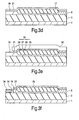
- a polysilicon layer 21 is then formed to a thickness of 1125 nm (11 250 ⁇ ) over the gate oxide layer 19 and the LOCOS layer 17 ( Figure 3d).
- the polysilicon layer 21 is then doped with in alternating bands of n and p type by implantation.
- An n-type gate region 23 is formed over the gate oxide layer and an n-p type field plate region 25 is formed over the graded drift region 13.
- a plurality of alternating n-type strips 27 and p-type strips 29 form a plurality of back-to back diodes 31 ( Figure 3e).
- a 2 ⁇ m thick resist layer 32 is formed, and patterned to leave the source region clear of resist, whilst protecting the rest of the structure.
- a two stage etch process removes the material above the source region. Firstly, a vertical dry etch is performed to etch to the top of the gate oxide, followed by an over etch which removes resist from below the edge of the mask with an undercut of 2 ⁇ m.
- An ADP implant is then performed to provide a high doping density body contact region 36 (Figure 3f).
- the resist is then stripped, and a low doping density body implant 34 performed.
- the low doping density implant forms the lightly doped p body implant self aligned to the edge of the gate polysilicon.
- the gate oxide layer 19 is stripped from the source region.
- a p-body anneal diffuses the dopant atoms from the lightly p-doped body under the polysilicon gate to form the body region 7 forming the channel.
- a screen oxide layer 12 is also grown on the source region.
- a dry etch process using a photolithographically defined mask removes the polysilicon layer 21 where not required.
- the mask in particular removes polysilicon from the drain region.
- the mask covers the source region during this step.
- a screen oxide layer 12 is then grown on the exposed drain region.
- n+ diffusion is then performed to define the source and drain regions.
- a further oxide layer 33 is then formed on the surface from tetra-ethyl-ortho-silicate (TEOS, also known as tetra-ethoxy silane), as is known.
- TEOS tetra-ethyl-ortho-silicate
- a plurality of contact vias 35 is formed in the TEOS oxide layer 33.
- a metallisation layer 37 is deposited on the TEOS layer, to form source 39, gate 41 and drain 43 connections.
- the source connection 39 extends to connect to both the source region 9 and the field plate region 25, as shown in Figure 4. As can be seen, the connection in the region of the source region connects to the high doping density body contact region 36 also.
- a rear contact 45 is provided on the backside of the substrate 1 to allow the substrate to be biased.
- the diodes act as protection diodes which are particularly suitable for protection against electrostatic discharge (ESD).
- the source connected field plate reduces the gate-drain capacitance C gd . This reduction is over and above the inherently low capacitance delivered by a silicon on insulator structure. Thus, the switching time of the device is reduced.
- the gate is protected from over-voltage and electrostatic discharge by the protection diodes formed between the gate region 23 and the field plate region 25 by the p-n junctions 26 in the semiconductor layer 21.
- the structure thus conveniently provides both good switching time and electrostatic discharge protection without adding significantly to the manufacturing complexity.
- the device can act as a RESURF structure in which the drift region 13 is wholly depleted when the device is turned off.
- the depletion region in the drift region 13 can extend into the drain region 11 and the low-doped body region 7. Voltage may be uniformly dropped across the depleted drift region allowing higher voltages to be present between source and drain before breakdown occurs.
- the doping of the drift region may be higher than would otherwise be compatible with completely depleting the drift region when the device is turned off. This in turn can decrease the on-resistance.
- the structure requires only a single polysilicon layer above the gate oxide and the LOCOS oxide which eases manufacture.
- the separation between field plate region 25 and gate region 23 is simply defined by the p and n strips, i.e. by the diffusions.
- the p-type strips may be lightly doped at or near the junction.
- the n-type strips may be lightly doped instead.
- the p+ region 36 near the source region 9 may improve the ruggedness of the structure. Further, it can act as an ohmic contact.
- the regions with p and n type doping may be switched around.
- the field plate region 25 may have the opposite polarity to the gate electrode 23 and the number of diodes of each polarity may be different.
- the gate insulation and field plate insulation need not be of oxide, but may be of other suitable materials, such as nitride.
- the semiconductor used is not restricted to silicon, but may also be gallium arsenide, or any other suitable semiconductor.
- the examples show a number of alternating p and n regions 27, 29 between the field plate region and the gate region, there may be more regions. Alternatively, there may be fewer regions. For example a single p region formed between an n-type gate region and an n-type field plate region will provide a single pair of back to back p-n junctions.
- Any suitable insulating layer may be used instead of the TEOS layers.
Landscapes
- Thin Film Transistor (AREA)
- Insulated Gate Type Field-Effect Transistor (AREA)
- Junction Field-Effect Transistors (AREA)
- Bipolar Transistors (AREA)
Claims (9)
- Transistor à effet de champ comprenant :une zone de source (9) et une zone de drain (11) latéralement espacées dans une couche de corps semi-conducteur (5) ;un canal et une zone de migration (13) dans la couche de corps semi-conducteur entre la zone de source et la zone de drain ;une couche d'oxyde (17, 19) sur le canal et la zone de migration ;une couche de semi-conducteur supérieure (21) formée sur la couche d'oxyde, la couche de semi-conducteur supérieure étant dopée pour avoir une zone de grille (23) formée sur le canal, une zone de plaque de champ (25) formée sur la zone de migration, et au moins une jonction P-N (26) formant au moins une diode entre la zone de plaque de champ et la zone de grille;caractérisé en ce queune interconnexion électrique (39) est formée entre la zone de source et la zone de plaque de champ pour connecter électriquement la zone de source et la zone de plaque de champ.
- Transistor selon la revendication 1, comprenant en outre un substrat (1) et une couche d'oxyde enterrée (3) sur le substrat et sous la couche de corps semi-conducteur.
- Transistor selon la revendication 1 ou 2, dans lequel la couche de semi-conducteur supérieure est dopée pour avoir une alternance de zones P et N (29, 27) formant une pluralité de diodes dos à dos.
- Transistor selon l'une quelconque des revendications précédentes, dans lequel la couche d'oxyde comprend une couche LOCOS (17) sur la zone de migration et une couche d'oxyde plus mince (19) sur le canal pour agir en tant qu'oxyde de grille.
- Transistor selon l'une quelconque des revendications précédentes, dans lequel la zone de migration a une concentration en agent dopant latéralement variable, avec une concentration en agent dopant plus forte à proximité de la zone de drain et une concentration en agent dopant plus faible à proximité du canal.
- Transistor à effet de champ à grille isolée selon l'une quelconque des revendications précédentes, dans lequel le niveau de dopage et l'épaisseur de la zone de migration sont tels que la zone de migration est appauvrie sur toute son épaisseur et sur toute sa longueur lorsque le transistor est mis hors tension.
- Procédé de fabrication d'un transistor à effet de champ comprenant, dans n'importe quel ordre, les étapes consistant à :- former une zone de migration dans une couche de corps semi-conducteur (5) ;- former une couche d'oxyde (17, 19) sur la couche de corps semi-conducteur (5);- déposer une couche de semi-conducteur supérieure (21) sur la couche d'oxyde ;- diffuser une alternance de zones de type P et de type N (29, 27) dans la couche de semi-conducteur supérieure pour former une zone de grille (23), une zone de plaque de champ (25) et au moins une jonction P-N (26) formant au moins une diode entre la zone de plaque de champ et la zone de grille, la zone de plaque de champ étant formée sur la zone de migration ;- diffuser les diffusions de source et de drain pour former une zone de source (9) et une zone de drain (11) dans la couche de corps semi-conducteur ; et- déposer une couche de métallisation définissant un contact de source (39) connecté à la zone de source et à la zone de plaque de champ, un contact de grille (41) connecté à la zone de grille et un contact de drain (43) connecté à la zone de drain.
- Procédé selon la revendication 7 comprenant la formation d'au moins une paire de diodes dos à dos entre la zone de plaque de champ et la zone de grille.
- Procédé selon la revendication 7 ou 8, comprenant en outre l'étape consistant à former la couche d'oxyde sur la zone de migration par oxydation locale de silicium (LOCOS).
Applications Claiming Priority (3)
| Application Number | Priority Date | Filing Date | Title |
|---|---|---|---|
| GB0107408 | 2001-03-23 | ||
| GBGB0107408.7A GB0107408D0 (en) | 2001-03-23 | 2001-03-23 | Field effect transistor structure and method of manufacture |
| PCT/IB2002/000970 WO2002078091A2 (fr) | 2001-03-23 | 2002-03-20 | Structure de transistor a effet de champ et son procede de production |
Publications (2)
| Publication Number | Publication Date |
|---|---|
| EP1378009A2 EP1378009A2 (fr) | 2004-01-07 |
| EP1378009B1 true EP1378009B1 (fr) | 2007-10-03 |
Family
ID=9911482
Family Applications (1)
| Application Number | Title | Priority Date | Filing Date |
|---|---|---|---|
| EP02708575A Expired - Lifetime EP1378009B1 (fr) | 2001-03-23 | 2002-03-20 | Structure de transistor a effet de champ et son procede de production |
Country Status (8)
| Country | Link |
|---|---|
| US (1) | US6677642B2 (fr) |
| EP (1) | EP1378009B1 (fr) |
| JP (1) | JP4157963B2 (fr) |
| KR (1) | KR20030005385A (fr) |
| AT (1) | ATE375008T1 (fr) |
| DE (1) | DE60222751T2 (fr) |
| GB (1) | GB0107408D0 (fr) |
| WO (1) | WO2002078091A2 (fr) |
Families Citing this family (39)
| Publication number | Priority date | Publication date | Assignee | Title |
|---|---|---|---|---|
| US6621138B1 (en) * | 2002-10-21 | 2003-09-16 | Micrel, Inc. | Zener-like trim device in polysilicon |
| US7501669B2 (en) | 2003-09-09 | 2009-03-10 | Cree, Inc. | Wide bandgap transistor devices with field plates |
| DE10345347A1 (de) * | 2003-09-19 | 2005-04-14 | Atmel Germany Gmbh | Verfahren zur Herstellung eines DMOS-Transistors mit lateralem Driftregionen-Dotierstoffprofil |
| SE0302810D0 (sv) * | 2003-10-24 | 2003-10-24 | Infineon Technologies Ag | Monolithically integrated circuit comprising a thin film resistor, and fabrication method thereof |
| JP4821090B2 (ja) * | 2004-03-23 | 2011-11-24 | セイコーエプソン株式会社 | 半導体装置の製造方法 |
| JP4618629B2 (ja) | 2004-04-21 | 2011-01-26 | 三菱電機株式会社 | 誘電体分離型半導体装置 |
| US7573078B2 (en) * | 2004-05-11 | 2009-08-11 | Cree, Inc. | Wide bandgap transistors with multiple field plates |
| US7550783B2 (en) * | 2004-05-11 | 2009-06-23 | Cree, Inc. | Wide bandgap HEMTs with source connected field plates |
| US9773877B2 (en) * | 2004-05-13 | 2017-09-26 | Cree, Inc. | Wide bandgap field effect transistors with source connected field plates |
| US11791385B2 (en) * | 2005-03-11 | 2023-10-17 | Wolfspeed, Inc. | Wide bandgap transistors with gate-source field plates |
| US7592211B2 (en) * | 2006-01-17 | 2009-09-22 | Cree, Inc. | Methods of fabricating transistors including supported gate electrodes |
| US7709269B2 (en) | 2006-01-17 | 2010-05-04 | Cree, Inc. | Methods of fabricating transistors including dielectrically-supported gate electrodes |
| DE102006023429B4 (de) * | 2006-05-18 | 2011-03-10 | Infineon Technologies Ag | ESD-Schutz-Element zur Verwendung in einem elektrischen Schaltkreis |
| US8823057B2 (en) | 2006-11-06 | 2014-09-02 | Cree, Inc. | Semiconductor devices including implanted regions for providing low-resistance contact to buried layers and related devices |
| US8283699B2 (en) | 2006-11-13 | 2012-10-09 | Cree, Inc. | GaN based HEMTs with buried field plates |
| US7692263B2 (en) | 2006-11-21 | 2010-04-06 | Cree, Inc. | High voltage GaN transistors |
| KR100848245B1 (ko) * | 2007-06-25 | 2008-07-24 | 주식회사 동부하이텍 | 반도체 소자 및 그 제조방법 |
| JP5206028B2 (ja) * | 2008-03-03 | 2013-06-12 | 株式会社デンソー | 半導体装置 |
| US20100117153A1 (en) * | 2008-11-07 | 2010-05-13 | Honeywell International Inc. | High voltage soi cmos device and method of manufacture |
| JP5748353B2 (ja) * | 2011-05-13 | 2015-07-15 | 株式会社豊田中央研究所 | 横型半導体装置 |
| JP5700027B2 (ja) * | 2012-12-07 | 2015-04-15 | トヨタ自動車株式会社 | 半導体装置 |
| JP6221284B2 (ja) * | 2013-03-19 | 2017-11-01 | 富士通セミコンダクター株式会社 | 半導体装置及び半導体装置の製造方法 |
| CN103325835B (zh) * | 2013-05-28 | 2015-10-21 | 电子科技大学 | 一种具有结型场板的soi功率ldmos器件 |
| US9755059B2 (en) | 2013-06-09 | 2017-09-05 | Cree, Inc. | Cascode structures with GaN cap layers |
| US9847411B2 (en) | 2013-06-09 | 2017-12-19 | Cree, Inc. | Recessed field plate transistor structures |
| US9679981B2 (en) | 2013-06-09 | 2017-06-13 | Cree, Inc. | Cascode structures for GaN HEMTs |
| US9236449B2 (en) * | 2013-07-11 | 2016-01-12 | Globalfoundries Inc. | High voltage laterally diffused metal oxide semiconductor |
| US9093568B1 (en) * | 2014-04-16 | 2015-07-28 | Infineon Technologies Ag | Semiconductor diode |
| CN104183646A (zh) * | 2014-08-29 | 2014-12-03 | 电子科技大学 | 一种具有延伸栅结构的soi ldmos器件 |
| CN104681621B (zh) | 2015-02-15 | 2017-10-24 | 上海华虹宏力半导体制造有限公司 | 一种源极抬高电压使用的高压ldmos及其制造方法 |
| CN105590960B (zh) * | 2015-12-28 | 2018-11-23 | 电子科技大学 | 横向绝缘栅双极型晶体管 |
| CN107680996A (zh) * | 2017-09-14 | 2018-02-09 | 电子科技大学 | 横向功率器件 |
| US10937872B1 (en) * | 2019-08-07 | 2021-03-02 | Vanguard International Semiconductor Corporation | Semiconductor structures |
| DE102019216138A1 (de) * | 2019-10-21 | 2021-04-22 | Robert Bosch Gmbh | Vertikaler feldeffekttransistor und verfahren zum ausbilden desselben |
| CN111725071B (zh) * | 2020-07-20 | 2021-06-18 | 西安电子科技大学 | 一种硅基结型积累层和缓冲层横向双扩散场效应晶体管及其制作方法 |
| CN112466955B (zh) * | 2020-12-04 | 2022-10-11 | 重庆邮电大学 | 一种具有体内导电沟道的薄层soi-ldmos器件 |
| KR102363450B1 (ko) * | 2020-12-22 | 2022-02-15 | (주) 트리노테크놀로지 | 클램핑 다이오드 및 클램핑 전압을 일정하게 유지하는 종단 구조 |
| CN116092944A (zh) * | 2023-02-28 | 2023-05-09 | 绍兴中芯集成电路制造股份有限公司 | 一种nldmos管及其制备方法 |
| CN116364782B (zh) * | 2023-04-27 | 2024-09-20 | 深圳市优恩半导体有限公司 | 栅极过压保护的芯片晶体管结构与制造方法 |
Family Cites Families (10)
| Publication number | Priority date | Publication date | Assignee | Title |
|---|---|---|---|---|
| US4810664A (en) * | 1986-08-14 | 1989-03-07 | Hewlett-Packard Company | Method for making patterned implanted buried oxide transistors and structures |
| US4922327A (en) * | 1987-12-24 | 1990-05-01 | University Of Toronto Innovations Foundation | Semiconductor LDMOS device with upper and lower passages |
| DE69209678T2 (de) | 1991-02-01 | 1996-10-10 | Philips Electronics Nv | Halbleiteranordnung für Hochspannungsverwendung und Verfahren zur Herstellung |
| US5246870A (en) | 1991-02-01 | 1993-09-21 | North American Philips Corporation | Method for making an improved high voltage thin film transistor having a linear doping profile |
| JP2906749B2 (ja) * | 1991-07-11 | 1999-06-21 | 日産自動車株式会社 | 半導体装置のゲート保護装置 |
| DE69225552T2 (de) * | 1991-10-15 | 1999-01-07 | Texas Instruments Inc., Dallas, Tex. | Lateraler doppel-diffundierter MOS-Transistor und Verfahren zu seiner Herstellung |
| JPH07326743A (ja) * | 1994-05-31 | 1995-12-12 | Fuji Electric Co Ltd | プレーナ型半導体素子 |
| KR100225411B1 (ko) * | 1997-03-24 | 1999-10-15 | 김덕중 | LDMOS(a lateral double-diffused MOS) 트랜지스터 소자 및 그의 제조 방법 |
| JP3315356B2 (ja) * | 1997-10-15 | 2002-08-19 | 株式会社東芝 | 高耐圧半導体装置 |
| KR100275758B1 (ko) * | 1998-12-17 | 2001-02-01 | 김덕중 | 제너 다이오드를 내장한 수평형 모스 게이트형 반도체 소자 및그 제조 방법 |
-
2001
- 2001-03-23 GB GBGB0107408.7A patent/GB0107408D0/en not_active Ceased
-
2002
- 2002-03-15 US US10/099,683 patent/US6677642B2/en not_active Expired - Lifetime
- 2002-03-20 JP JP2002576022A patent/JP4157963B2/ja not_active Expired - Fee Related
- 2002-03-20 WO PCT/IB2002/000970 patent/WO2002078091A2/fr not_active Ceased
- 2002-03-20 DE DE60222751T patent/DE60222751T2/de not_active Expired - Lifetime
- 2002-03-20 AT AT02708575T patent/ATE375008T1/de not_active IP Right Cessation
- 2002-03-20 EP EP02708575A patent/EP1378009B1/fr not_active Expired - Lifetime
- 2002-03-20 KR KR1020027015815A patent/KR20030005385A/ko not_active Withdrawn
Non-Patent Citations (1)
| Title |
|---|
| None * |
Also Published As
| Publication number | Publication date |
|---|---|
| US20020137318A1 (en) | 2002-09-26 |
| DE60222751D1 (de) | 2007-11-15 |
| JP2004519862A (ja) | 2004-07-02 |
| JP4157963B2 (ja) | 2008-10-01 |
| GB0107408D0 (en) | 2001-05-16 |
| US6677642B2 (en) | 2004-01-13 |
| ATE375008T1 (de) | 2007-10-15 |
| EP1378009A2 (fr) | 2004-01-07 |
| WO2002078091A2 (fr) | 2002-10-03 |
| DE60222751T2 (de) | 2008-07-17 |
| WO2002078091A3 (fr) | 2003-05-30 |
| KR20030005385A (ko) | 2003-01-17 |
Similar Documents
| Publication | Publication Date | Title |
|---|---|---|
| EP1378009B1 (fr) | Structure de transistor a effet de champ et son procede de production | |
| US5614751A (en) | Edge termination structure for power MOSFET | |
| US5629552A (en) | Stable high voltage semiconductor device structure | |
| KR100816253B1 (ko) | 트렌치 게이트 전계 효과 트랜지스터 및 그의 제조 방법 | |
| EP0562271B1 (fr) | Structure haute tension avec source isolée par oxyde et région RESURF de drift dans du silicon massif | |
| US4247860A (en) | MIS Field effect transistor for high source-drain voltages | |
| US6091086A (en) | Reverse blocking IGBT | |
| US5382536A (en) | Method of fabricating lateral DMOS structure | |
| US6664593B2 (en) | Field effect transistor structure and method of manufacture | |
| KR20100036978A (ko) | 트랜지스터-타입 보호 장치, 반도체 집적 회로, 및 그의 제조 방법 | |
| US6773997B2 (en) | Method for manufacturing a high voltage MOSFET semiconductor device with enhanced charge controllability | |
| US7074681B2 (en) | Semiconductor component and method of manufacturing | |
| KR100722012B1 (ko) | 반도체 디바이스 | |
| EP0772241B1 (fr) | Dispositif de puissance à haute densité en technologie MOS | |
| US6420767B1 (en) | Capacitively coupled DTMOS on SOI | |
| US20240063777A1 (en) | Hvic device with combined level shifter and boost diode in junction termination region | |
| US20020185695A1 (en) | Lateral DMOS structure with lateral extension structure for reduced charge trapping in gate oxide | |
| US5962898A (en) | Field-effect transistor | |
| US20250142880A1 (en) | Field effect transistor having an electrode trench structure | |
| JPH07183545A (ja) | 半導体素子 |
Legal Events
| Date | Code | Title | Description |
|---|---|---|---|
| PUAI | Public reference made under article 153(3) epc to a published international application that has entered the european phase |
Free format text: ORIGINAL CODE: 0009012 |
|
| AK | Designated contracting states |
Kind code of ref document: A2 Designated state(s): AT BE CH CY DE DK ES FI FR GB GR IE IT LI LU MC NL PT SE TR |
|
| 17P | Request for examination filed |
Effective date: 20031201 |
|
| GRAP | Despatch of communication of intention to grant a patent |
Free format text: ORIGINAL CODE: EPIDOSNIGR1 |
|
| RAP1 | Party data changed (applicant data changed or rights of an application transferred) |
Owner name: NXP B.V. |
|
| GRAS | Grant fee paid |
Free format text: ORIGINAL CODE: EPIDOSNIGR3 |
|
| GRAA | (expected) grant |
Free format text: ORIGINAL CODE: 0009210 |
|
| AK | Designated contracting states |
Kind code of ref document: B1 Designated state(s): AT BE CH CY DE DK ES FI FR GB GR IE IT LI LU MC NL PT SE TR |
|
| REG | Reference to a national code |
Ref country code: GB Ref legal event code: FG4D |
|
| REG | Reference to a national code |
Ref country code: CH Ref legal event code: EP |
|
| REG | Reference to a national code |
Ref country code: IE Ref legal event code: FG4D |
|
| REF | Corresponds to: |
Ref document number: 60222751 Country of ref document: DE Date of ref document: 20071115 Kind code of ref document: P |
|
| NLV1 | Nl: lapsed or annulled due to failure to fulfill the requirements of art. 29p and 29m of the patents act | ||
| REG | Reference to a national code |
Ref country code: CH Ref legal event code: PL |
|
| PG25 | Lapsed in a contracting state [announced via postgrant information from national office to epo] |
Ref country code: SE Free format text: LAPSE BECAUSE OF FAILURE TO SUBMIT A TRANSLATION OF THE DESCRIPTION OR TO PAY THE FEE WITHIN THE PRESCRIBED TIME-LIMIT Effective date: 20080103 Ref country code: NL Free format text: LAPSE BECAUSE OF FAILURE TO SUBMIT A TRANSLATION OF THE DESCRIPTION OR TO PAY THE FEE WITHIN THE PRESCRIBED TIME-LIMIT Effective date: 20071003 Ref country code: LI Free format text: LAPSE BECAUSE OF FAILURE TO SUBMIT A TRANSLATION OF THE DESCRIPTION OR TO PAY THE FEE WITHIN THE PRESCRIBED TIME-LIMIT Effective date: 20071003 Ref country code: ES Free format text: LAPSE BECAUSE OF FAILURE TO SUBMIT A TRANSLATION OF THE DESCRIPTION OR TO PAY THE FEE WITHIN THE PRESCRIBED TIME-LIMIT Effective date: 20080114 Ref country code: CH Free format text: LAPSE BECAUSE OF FAILURE TO SUBMIT A TRANSLATION OF THE DESCRIPTION OR TO PAY THE FEE WITHIN THE PRESCRIBED TIME-LIMIT Effective date: 20071003 |
|
| PG25 | Lapsed in a contracting state [announced via postgrant information from national office to epo] |
Ref country code: PT Free format text: LAPSE BECAUSE OF FAILURE TO SUBMIT A TRANSLATION OF THE DESCRIPTION OR TO PAY THE FEE WITHIN THE PRESCRIBED TIME-LIMIT Effective date: 20080303 |
|
| ET | Fr: translation filed | ||
| PG25 | Lapsed in a contracting state [announced via postgrant information from national office to epo] |
Ref country code: AT Free format text: LAPSE BECAUSE OF FAILURE TO SUBMIT A TRANSLATION OF THE DESCRIPTION OR TO PAY THE FEE WITHIN THE PRESCRIBED TIME-LIMIT Effective date: 20071003 |
|
| PG25 | Lapsed in a contracting state [announced via postgrant information from national office to epo] |
Ref country code: DK Free format text: LAPSE BECAUSE OF FAILURE TO SUBMIT A TRANSLATION OF THE DESCRIPTION OR TO PAY THE FEE WITHIN THE PRESCRIBED TIME-LIMIT Effective date: 20071003 |
|
| PLBE | No opposition filed within time limit |
Free format text: ORIGINAL CODE: 0009261 |
|
| STAA | Information on the status of an ep patent application or granted ep patent |
Free format text: STATUS: NO OPPOSITION FILED WITHIN TIME LIMIT |
|
| PG25 | Lapsed in a contracting state [announced via postgrant information from national office to epo] |
Ref country code: BE Free format text: LAPSE BECAUSE OF FAILURE TO SUBMIT A TRANSLATION OF THE DESCRIPTION OR TO PAY THE FEE WITHIN THE PRESCRIBED TIME-LIMIT Effective date: 20071003 |
|
| 26N | No opposition filed |
Effective date: 20080704 |
|
| PG25 | Lapsed in a contracting state [announced via postgrant information from national office to epo] |
Ref country code: MC Free format text: LAPSE BECAUSE OF NON-PAYMENT OF DUE FEES Effective date: 20080331 |
|
| PG25 | Lapsed in a contracting state [announced via postgrant information from national office to epo] |
Ref country code: IE Free format text: LAPSE BECAUSE OF NON-PAYMENT OF DUE FEES Effective date: 20080320 Ref country code: GR Free format text: LAPSE BECAUSE OF FAILURE TO SUBMIT A TRANSLATION OF THE DESCRIPTION OR TO PAY THE FEE WITHIN THE PRESCRIBED TIME-LIMIT Effective date: 20080104 |
|
| PG25 | Lapsed in a contracting state [announced via postgrant information from national office to epo] |
Ref country code: CY Free format text: LAPSE BECAUSE OF FAILURE TO SUBMIT A TRANSLATION OF THE DESCRIPTION OR TO PAY THE FEE WITHIN THE PRESCRIBED TIME-LIMIT Effective date: 20071003 |
|
| PG25 | Lapsed in a contracting state [announced via postgrant information from national office to epo] |
Ref country code: FI Free format text: LAPSE BECAUSE OF FAILURE TO SUBMIT A TRANSLATION OF THE DESCRIPTION OR TO PAY THE FEE WITHIN THE PRESCRIBED TIME-LIMIT Effective date: 20071003 |
|
| PG25 | Lapsed in a contracting state [announced via postgrant information from national office to epo] |
Ref country code: LU Free format text: LAPSE BECAUSE OF NON-PAYMENT OF DUE FEES Effective date: 20080320 |
|
| PG25 | Lapsed in a contracting state [announced via postgrant information from national office to epo] |
Ref country code: TR Free format text: LAPSE BECAUSE OF FAILURE TO SUBMIT A TRANSLATION OF THE DESCRIPTION OR TO PAY THE FEE WITHIN THE PRESCRIBED TIME-LIMIT Effective date: 20071003 |
|
| PG25 | Lapsed in a contracting state [announced via postgrant information from national office to epo] |
Ref country code: IT Free format text: LAPSE BECAUSE OF NON-PAYMENT OF DUE FEES Effective date: 20080331 |
|
| REG | Reference to a national code |
Ref country code: DE Ref legal event code: R084 Ref document number: 60222751 Country of ref document: DE |
|
| REG | Reference to a national code |
Ref country code: DE Ref legal event code: R084 Ref document number: 60222751 Country of ref document: DE Effective date: 20141015 |
|
| REG | Reference to a national code |
Ref country code: FR Ref legal event code: PLFP Year of fee payment: 14 |
|
| REG | Reference to a national code |
Ref country code: FR Ref legal event code: PLFP Year of fee payment: 15 |
|
| REG | Reference to a national code |
Ref country code: FR Ref legal event code: PLFP Year of fee payment: 16 |
|
| REG | Reference to a national code |
Ref country code: FR Ref legal event code: PLFP Year of fee payment: 17 |
|
| PGFP | Annual fee paid to national office [announced via postgrant information from national office to epo] |
Ref country code: DE Payment date: 20200218 Year of fee payment: 19 Ref country code: GB Payment date: 20200221 Year of fee payment: 19 |
|
| PGFP | Annual fee paid to national office [announced via postgrant information from national office to epo] |
Ref country code: FR Payment date: 20200220 Year of fee payment: 19 |
|
| REG | Reference to a national code |
Ref country code: DE Ref legal event code: R119 Ref document number: 60222751 Country of ref document: DE |
|
| GBPC | Gb: european patent ceased through non-payment of renewal fee |
Effective date: 20210320 |
|
| PG25 | Lapsed in a contracting state [announced via postgrant information from national office to epo] |
Ref country code: DE Free format text: LAPSE BECAUSE OF NON-PAYMENT OF DUE FEES Effective date: 20211001 Ref country code: FR Free format text: LAPSE BECAUSE OF NON-PAYMENT OF DUE FEES Effective date: 20210331 Ref country code: GB Free format text: LAPSE BECAUSE OF NON-PAYMENT OF DUE FEES Effective date: 20210320 |