EP1378773A2 - Coupleur de guides d'ondes optiques - Google Patents
Coupleur de guides d'ondes optiques Download PDFInfo
- Publication number
- EP1378773A2 EP1378773A2 EP03254154A EP03254154A EP1378773A2 EP 1378773 A2 EP1378773 A2 EP 1378773A2 EP 03254154 A EP03254154 A EP 03254154A EP 03254154 A EP03254154 A EP 03254154A EP 1378773 A2 EP1378773 A2 EP 1378773A2
- Authority
- EP
- European Patent Office
- Prior art keywords
- optical waveguide
- optical
- circuit device
- polymeric
- waveguide coupler
- Prior art date
- Legal status (The legal status is an assumption and is not a legal conclusion. Google has not performed a legal analysis and makes no representation as to the accuracy of the status listed.)
- Withdrawn
Links
- 230000003287 optical effect Effects 0.000 title claims abstract description 179
- 238000005253 cladding Methods 0.000 claims abstract description 41
- 239000000758 substrate Substances 0.000 claims abstract description 33
- VYPSYNLAJGMNEJ-UHFFFAOYSA-N silicon dioxide Inorganic materials O=[Si]=O VYPSYNLAJGMNEJ-UHFFFAOYSA-N 0.000 claims description 23
- 229920000642 polymer Polymers 0.000 claims description 19
- 239000010453 quartz Substances 0.000 claims description 19
- XUIMIQQOPSSXEZ-UHFFFAOYSA-N Silicon Chemical compound [Si] XUIMIQQOPSSXEZ-UHFFFAOYSA-N 0.000 claims description 10
- 229910052710 silicon Inorganic materials 0.000 claims description 10
- 239000010703 silicon Substances 0.000 claims description 10
- 229920001721 polyimide Polymers 0.000 claims description 5
- 239000009719 polyimide resin Substances 0.000 claims description 4
- 230000010287 polarization Effects 0.000 abstract description 35
- 239000010410 layer Substances 0.000 description 31
- 235000012239 silicon dioxide Nutrition 0.000 description 19
- 230000008859 change Effects 0.000 description 12
- 238000000034 method Methods 0.000 description 11
- 230000001419 dependent effect Effects 0.000 description 6
- 238000004519 manufacturing process Methods 0.000 description 6
- 239000000463 material Substances 0.000 description 6
- 238000004891 communication Methods 0.000 description 5
- 150000004985 diamines Chemical class 0.000 description 4
- 230000000694 effects Effects 0.000 description 4
- 239000000835 fiber Substances 0.000 description 4
- 239000000969 carrier Substances 0.000 description 3
- 239000012792 core layer Substances 0.000 description 3
- 230000008878 coupling Effects 0.000 description 3
- 238000010168 coupling process Methods 0.000 description 3
- 238000005859 coupling reaction Methods 0.000 description 3
- 238000010438 heat treatment Methods 0.000 description 3
- 239000002904 solvent Substances 0.000 description 3
- 238000004528 spin coating Methods 0.000 description 3
- QHHKLPCQTTWFSS-UHFFFAOYSA-N 5-[2-(1,3-dioxo-2-benzofuran-5-yl)-1,1,1,3,3,3-hexafluoropropan-2-yl]-2-benzofuran-1,3-dione Chemical compound C1=C2C(=O)OC(=O)C2=CC(C(C=2C=C3C(=O)OC(=O)C3=CC=2)(C(F)(F)F)C(F)(F)F)=C1 QHHKLPCQTTWFSS-UHFFFAOYSA-N 0.000 description 2
- IJGRMHOSHXDMSA-UHFFFAOYSA-N Atomic nitrogen Chemical compound N#N IJGRMHOSHXDMSA-UHFFFAOYSA-N 0.000 description 2
- 230000004075 alteration Effects 0.000 description 2
- 230000008901 benefit Effects 0.000 description 2
- 230000005540 biological transmission Effects 0.000 description 2
- 230000015572 biosynthetic process Effects 0.000 description 2
- 238000004364 calculation method Methods 0.000 description 2
- 238000009826 distribution Methods 0.000 description 2
- 238000005516 engineering process Methods 0.000 description 2
- 239000002861 polymer material Substances 0.000 description 2
- 239000000377 silicon dioxide Substances 0.000 description 2
- HLBLWEWZXPIGSM-UHFFFAOYSA-N 4-Aminophenyl ether Chemical compound C1=CC(N)=CC=C1OC1=CC=C(N)C=C1 HLBLWEWZXPIGSM-UHFFFAOYSA-N 0.000 description 1
- NVKGJHAQGWCWDI-UHFFFAOYSA-N 4-[4-amino-2-(trifluoromethyl)phenyl]-3-(trifluoromethyl)aniline Chemical group FC(F)(F)C1=CC(N)=CC=C1C1=CC=C(N)C=C1C(F)(F)F NVKGJHAQGWCWDI-UHFFFAOYSA-N 0.000 description 1
- MYMOFIZGZYHOMD-UHFFFAOYSA-N Dioxygen Chemical compound O=O MYMOFIZGZYHOMD-UHFFFAOYSA-N 0.000 description 1
- FXHOOIRPVKKKFG-UHFFFAOYSA-N N,N-Dimethylacetamide Chemical compound CN(C)C(C)=O FXHOOIRPVKKKFG-UHFFFAOYSA-N 0.000 description 1
- 239000004642 Polyimide Substances 0.000 description 1
- 229910052799 carbon Inorganic materials 0.000 description 1
- 238000010276 construction Methods 0.000 description 1
- 238000007796 conventional method Methods 0.000 description 1
- 238000013461 design Methods 0.000 description 1
- 229910001882 dioxygen Inorganic materials 0.000 description 1
- 238000011156 evaluation Methods 0.000 description 1
- 238000000605 extraction Methods 0.000 description 1
- 238000012423 maintenance Methods 0.000 description 1
- 238000005259 measurement Methods 0.000 description 1
- 229910052757 nitrogen Inorganic materials 0.000 description 1
- 238000005457 optimization Methods 0.000 description 1
- 238000011056 performance test Methods 0.000 description 1
- 238000001020 plasma etching Methods 0.000 description 1
- 230000008569 process Effects 0.000 description 1
- 238000012545 processing Methods 0.000 description 1
- 238000005070 sampling Methods 0.000 description 1
- 239000004065 semiconductor Substances 0.000 description 1
- 229910052717 sulfur Inorganic materials 0.000 description 1
- 239000013589 supplement Substances 0.000 description 1
- 238000012360 testing method Methods 0.000 description 1
Images


Classifications
-
- G—PHYSICS
- G02—OPTICS
- G02B—OPTICAL ELEMENTS, SYSTEMS OR APPARATUS
- G02B6/00—Light guides; Structural details of arrangements comprising light guides and other optical elements, e.g. couplings
- G02B6/10—Light guides; Structural details of arrangements comprising light guides and other optical elements, e.g. couplings of the optical waveguide type
- G02B6/12—Light guides; Structural details of arrangements comprising light guides and other optical elements, e.g. couplings of the optical waveguide type of the integrated circuit kind
-
- G—PHYSICS
- G02—OPTICS
- G02B—OPTICAL ELEMENTS, SYSTEMS OR APPARATUS
- G02B6/00—Light guides; Structural details of arrangements comprising light guides and other optical elements, e.g. couplings
- G02B6/10—Light guides; Structural details of arrangements comprising light guides and other optical elements, e.g. couplings of the optical waveguide type
- G02B6/12—Light guides; Structural details of arrangements comprising light guides and other optical elements, e.g. couplings of the optical waveguide type of the integrated circuit kind
- G02B6/122—Basic optical elements, e.g. light-guiding paths
- G02B6/1221—Basic optical elements, e.g. light-guiding paths made from organic materials
-
- G—PHYSICS
- G02—OPTICS
- G02B—OPTICAL ELEMENTS, SYSTEMS OR APPARATUS
- G02B6/00—Light guides; Structural details of arrangements comprising light guides and other optical elements, e.g. couplings
- G02B6/10—Light guides; Structural details of arrangements comprising light guides and other optical elements, e.g. couplings of the optical waveguide type
- G02B6/12—Light guides; Structural details of arrangements comprising light guides and other optical elements, e.g. couplings of the optical waveguide type of the integrated circuit kind
- G02B6/12007—Light guides; Structural details of arrangements comprising light guides and other optical elements, e.g. couplings of the optical waveguide type of the integrated circuit kind forming wavelength selective elements, e.g. multiplexer, demultiplexer
Definitions
- the present invention relates to a polymer-based optical waveguide circuit stable to the changes of particularly, a polarization and ambient temperature which is profitably used as a wavelength division multiplexer or demultiplexer in, for example, fiber optic communication.
- the wavelength independent waveguide coupler In a dense wavelength division multiplexing (DWDM) system applied to optical carriers belonging to S, C and L bands, the wavelength independent waveguide coupler has been used that is capable of routing optical carriers comprising 80-100 nm bands around 1550 nm into two channels at a specified split ratio, being unaffected with their wavelengths.
- the coupler that routes optical carriers at a split ratio of 1:1 is called a 3 dB coupler and has been used in multiple fiber optic communication systems.
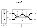
- Such a wavelength independent waveguide coupler includes a Mach-Zehnder interferometer type optical circuit 17 as shown in Fig. 9.
- the circuit comprises two waveguide cores 13, 14 formed on the surface of a substrate 20 prepared from a quartz or silicon wafer.
- the waveguide cores 13, 14 are covered with lower and upper cladding layers 18, 19 both of which are formed on the substrate 20.
- the core and cladding layers are mainly composed of silicon dioxide (SiO 2 )
- the resulting optical circuit is called a quartz waveguide.
- they are composed of a polymer
- the resulting optical circuit is called a polymeric waveguide.
- the Mach-Zehnder interferometer type optical circuit 17 comprises two directional couplers 15, 16 which are obtained by bringing the two waveguide cores 13, 14 close to and in parallel with each other.
- the Mach-Zehnder interferometer type optical circuit 17 receives an optical signal having a band width of 80-100 nm around 1550 nm either from a terminal 13a or 14a connected respectively to the waveguide core 13 or 14 and splits the signal at a split ratio of 1:1 to deliver two outputs each having an intensity half that of the transmitted signal from terminals 13b, 14b, or the other terminals of the waveguide cores 13, 14.
- An application of such a Mach-Zender interferometer type optical circuit 17 includes 2 ⁇ 2N splitter as shown in Fig 2.
- the 2 ⁇ 2N splitter comprises 3 dB coupler 9 independent of its wavelength with a waveguide circuit same as a Mach-Zender inteferometer type optical circuit 17,and a waveguide branch circuit 10 having paralleled two 1 ⁇ 2N splitter in series with said coupler 9.
- This 2 ⁇ 2N splitter as shown in Fig 2 achieves a function of light power splitter with a wave band required for DWDM.
- the 2 ⁇ 2N splitter shown in Fig 2 includes the waveguides made from a polymer, its optical characteristics are apt to vary in the presence of changes of the ambient temperature, and thus the temperature range under which it can normally operate is rather limited. Further a polymer has a birefringence and the characteristics are apt to vary in the presence of the direction of light polarization used. Thus the loss characteristics dependent of polarization (PDL) is rather worse.
- PDL loss characteristics dependent of polarization
- said waveguide branch circuit 10 of the rear part of the 2 ⁇ 2N splitter shown in Fig 2 made from a polymer waveguides are unaffected by the ambient temperature and the change of the polarization.(Bao-Xue Chen et al, " Optical Coupler” , US Patent 5757995). Therefore the 3dB coupler 9 independent of wavelength of the front part of the 2 ⁇ 2N splitter shown in Fig. 2 should be carefully designed.
- the temperature coefficient of the refractive index of a polymer material used for the construction of the waveguides is ten or more times as high as that of quartz and its birefringence (a double refraction) is about 0.0082, as that of quartz is about Zero.
- the polymeric waveguides 9, 10 and cladding layers covering those waveguides will undergo a great change in their refractive indices; the parameters of the optical circuit including those waveguides and cladding layers will also shift from the designed ranges, and the performance of the optical circuit will depart from the designed level.
- a equivalent refraction of a waveguide is modified due to a effect of a birefringence (a double refraction) in the presence of a change of a polarization plane of a input signal. Therefore, because a complete combination length of two directional couplers 15 and 16, and a phase difference which is produced as a result of properly chosen path length difference between the two waveguide cores 13 and 14 will change, a power distribution ratio will shift from the designed ranges.
- a known method for preparing an optical waveguide circuit from quartz consists of covering a quartz waveguide core with a polymeric coat whose refractive index has a negative temperature coefficient sufficiently large to cancel the positivity of the temperature coefficient of the quartz waveguide core.
- a polymeric material has a refractive index whose temperature coefficient has too large a negative value to cancel the positivity of the temperature coefficient of a quartz material.
- this method can not be applied for the polymeric optical waveguide circuit here concerned.
- a known method for compensating for the thermal characteristics of a polymeric waveguide core is to employ a substrate made from a polymer having a high thermal expansion.
- this method consists of employing a polymeric substrate which has a thermal expansion sufficiently high to cancel the negative temperature coefficient of the refractive index of a polymeric waveguide core.
- a substrate made from quartz or silicon generally has a low thermal expansion, and thus as far as based on this method, it will not be possible to integrate optical waveguide circuits on a silicon substrate as in the conventional electronic technology where semiconductor devices are integrated on a silicon substrate.
- the method for canceling a characteristics dependent of polarization is being proposed; providing recess in a cross section of a waveguide and inserting wave plate of a thin layer in said recess, and rotating rectangularly a polarization plane and canceling an effect of a rotation.
- This circuit is used in a symmetric structure such as AWG, but is not applied to a coupler which achieves performance independent of wavelength by means of asymmetric of light waveguide circuit.
- a requirement for providing a recess and inserting wave plate in its manufacturing process is so complicate and severe.
- microscope processing is necessary and a extraction rate, i.e, a yielding percentage is worse and its production cost is high.
- the object of the present invention is to provide a Mach-Zehnder interferometer-based polymeric waveguide circuit unaffected with the change of polarization and ambient temperature which is obtainable by arranging waveguides on a silicon or quartz substrate using conventional IC technology, while maintaining the advantage of low production cost which is the most important impetus for the introduction of polymeric optical waveguide circuits.
- the optical waveguide coupler circuit give priority to a characteristics dependent of temperature or give priority to both the characteristics dependent of temperature and polarization.
- Inventors of this application previously proposed a polymeric optical waveguide coupler circuit which could suppress the fluctuation of output which is produced as a result of change of ambient temperature, taking into account of the characteristics independent of temperature.
- a further aspect of the present invention is to provide an optical waveguide coupler circuit device comprising the polymeric optical waveguide is made from a polymer having a refractive index of 1.508 to 1.568 and a birefringence (a double refraction) of 0.008 to 0.01.
- a further aspect of the present invention is to provide optical waveguide coupler circuit device comprising the polymeric lower cladding layer is made from a polymer having a refractive index of 1.503 to 1.562 and a birefringence (a double refraction) of 0.008 to 0.01.
- a further aspect of the present invention is to provide an optical waveguide coupler circuit device comprising the polymeric upper cladding layer is made from a polymer having a refractive index of 1.503 to 1.562 and a birefringence (a double refraction) of 0.008 to 0.01.
- a further aspect of the present invention is to provide an optical waveguide coupler circuit device wherein the length of the two optical waveguides of one directional coupler is chosen to be 0.101 to 0.128 mm while the length of the two optical waveguides of the other directional coupler is chosen to be 1.454 to 1.612 mm.
- a further aspect of the present invention is to provide an optical waveguide coupler circuit device wherein the gap between two parallel running waveguides is chosen to be 4.3 to 5.1 ⁇ m for both directional couplers.
- a further aspect of the present invention is to provide an optical waveguide coupler circuit device wherein each of the optical waveguides is configured to have an oblong cross-section having a width w and a thickness t.
- a further aspect of the present invention is to provide an optical waveguide coupler circuit device wherein each of the optical waveguides is configured to have a square cross-section.
- a further aspect of the present invention is to provide an optical waveguide coupler circuit device wherein each of the optical waveguides is configured to have a square cross-section with a side of 6 to 8 ⁇ m.
- a further aspect of the present invention is to provide an optical waveguide coupler circuit device wherein a lower cladding layer of the optical waveguides is configured to have a thickness of 20 ⁇ m.
- a further aspect of the invention is to provide an optical waveguide coupler circuit device wherein the substrate is made of a quartz plate.
- a further aspect of the present invention is to provide an optical waveguide coupler circuit device wherein the substrate is made of a silicon plate.
- a further aspect of the present invention is to provide an optical waveguide coupler circuit device wherein the substrate is made of a polyimide resin plate.
- a polymeric optical waveguide coupler circuit devise 8 stable to the changes of polarized light and ambient temperature representing an embodiment of this invention and shown in Fig. 1
- Fig. 1 comprises two optical waveguide cores 2, 3 formed on the surface of a substrate 1 prepared from a quartz plate, a silicon wafer or a polyimide resin plate and the like.
- the optical waveguide cores 2, 3 are covered by a lower cladding layer 6 and an upper cladding layer 7 both being formed on the substrate 1.
- the devise 8 further comprises two directional couplers 4, 5 each of which is obtained by bringing the two optical waveguides 2, 3 close to and in parallel with each other.
- the cross-sections and refractive indices of the optical waveguide cores 2, 3, and other circuit parameters are optimized such that the performance of the device is maintained even when light passing through the device undergoes a shift in its wavelength, the polarized light or the ambient temperature is changed.
- a out and B out represent the amplitudes of the light waves delivered as outputs from the terminals 2b, 3b of the optical waveguide cores 2, 3,
- the transmission constant can be expressed as a function of the following parameters: the wavelength of a light wave, w and t; the width and thickness of the optical waveguide cores 2, 3, n g ; the refractive index of the optical waveguide cores 2, 3, and n c ;the refractive index of the cladding layers 6, 7, as follows.
- ⁇ ⁇ ( ⁇ , w, t, n g , n c )
- ⁇ ( ⁇ ,T) ⁇ ⁇ ⁇ ⁇ ⁇ ⁇
- the resulting optical waveguide circuit will split a light wave at a specified split ratio independent of its wavelength, and being unaffected by the ambient temperature.
- ⁇ ⁇ and ⁇ T are chosen so as to make ⁇ 1%.
- the optical waveguide circuit 8 shown in Fig. 1 can have periodically changing outputs, and thus numerous sets of optimized parameters are conceivable for a given single mode of polarized light waves. If TE and TM modes are conceivable for each light wave, the set of optimized parameters will be doubled.
- the optical waveguide circuit having its parameters optimized for splitting a given light wave independent of its wavelength being unaffected by the change of ambient temperature, is further optimized for the polarization of the light wave.
- statistical optimization is employed.
- ⁇ lmn is a power split ratio obtained as a result of the above calculation
- Q a target value in design
- D lmn a difference between ⁇ lmn and Q.
- l 1, 2 represent TE and TM modes respectively
- m and n represent the sampling numbers of temperature and wavelength respectively.
- the evaluation function statistically representing the agreement between a calculated value and the target value can be expressed by the following equation.
- the coupler device When the involved parameters are chosen to minimize ⁇ of the equation (14), and a polymeric optical waveguide coupler device is prepared based on the thus chosen parameters, the coupler device will split an incoming light wave at a specified split ratio independent of its wavelength and polarization, being unaffected by the ambient temperature.
- the polymeric optical waveguide coupler circuit 8 stable to ambient temperature changes produced by the above method according to this invention has its parameters optimized as described below.
- its substrate 1 is made from quartz, silicon or a polyimide resin and the like; the optical waveguides 2, 3 from a polymer having a refractive index ng of 1.508 to 1.568 and a birefringence (a double refraction) of 0.008 to 0.01 and the lower and upper cladding layers 6, 7 for covering the optical waveguides 2, 3 from another polymer having a refractive index n c of 1.503 to 1.562 and a birefringence (a double refraction) of 0.008 to 0.01 at 1550nm wavelength.
- Each of the optical waveguides 2, 3 has a square cross-section with a side of 6 to 8 ⁇ m;
- the parallel section of the directional coupler 4 has a length L 1 of 0.101 to 0.128 or 1.454 to 1.612 mm;
- the parallel section of the directional coupler 5 has a length L 2 of 1.454 to 1.612 or 0.101 to 0.128 mm;
- the gap of the parallel waveguides in the directional coupler 4 has a size S 1 of 4.3 to 5.1 ⁇ m;
- the gap of the parallel waveguides in the directional coupler 5 has a size S 2 of 4.3 to 5.1 ⁇ m;
- the optical path difference ⁇ L between the two optical waveguides 2, 3 is 0.7 to 0.9 ⁇ m.
- Fig. 1 shows an optical waveguide coupler circuit device of this invention.
- the polymeric optical waveguide coupler circuit device 8 stable to the changes of ambient temperature comprises two optical waveguide cores 2, 3 formed on the surface of a substrate 1 made of a quartz plate as shown in Fig. 1.
- the optical waveguide cores 2, 3 are made from a polymer material having a refractive index n g of 1.508 to 1.568 and a double refraction of 0.008 to 0.01 as shown in the figure, and has a square cross-section with a side of 6 to 8 ⁇ m.
- the material constituting the lower and upper cladding layers 6, 7 covering the optical waveguide cores 2, 3 is a polymer having a refractive index n c of 1.503 to 1.562 and a double refraction of 0.008 to 0.01.
- the optical waveguide cores 2, 3 form two directional couplers 4, 5 by approaching to and running in parallel with each other at two sites.
- the length L 1 of the parallel section is 0.101 to 0.128 mm (or 1.454 to 1.612mm), and the gap S 1 between the parallel running waveguides is 4.3 to 5.1 ⁇ m.
- the corresponding length L 2 and gap S 2 are 1.454 to 1.612 mm(or 0.101 to 0.128mm) and 4.3 to 5.1 ⁇ m, respectively.
- the optical waveguide cores 2, 3 are configured such that the difference between their optical path lengths falls within 0.7 to 0.9 ⁇ m.
- a quartz plate to serve as a substrate 1 is prepared.
- a solution of a polymer which will form a lower cladding layer is prepared by dissolving the same molecular amounts of 4,4'-(hexafluoroisopropylidene)diphthalic anhydride and 2,2'-bis(trifluoromethyl)-4,4'-diaminobiphenyl in N,N-dimethylacetamide, and the solution is stirred at 25°C for 24 hours in the presence of nitrogen.
- the resulting solution is applied by spin coating onto the substrate 1 to form a coat thereupon.
- the assembly is removed of the solvent, and subjected to a heating treatment, to form a polymeric lower cladding layer 6 having a thickness of about 20 mm on the substrate 1.
- a solution of another polymer is prepared as follows: part of diamine that has been used for producing the polymer responsible for the formation of the lower cladding layer, that is, part of 2,2'-bis(trifluoromethyl)-4,4'-diamonobiphenyl is substituted for another diamine, that is, 4,4'-diaminodiphenyl ether, and the two diamines are added to 4,4'-(hexafluoroisopropylidene)diphthalic anhydride such that the summed molecular amounts of the two diamines are equal to the molecular amount of the latter.
- the resulting solution is treated as above, and is applied by spin coating onto the above assembly to form a coat on the coat to serve as the lower cladding layer.
- the assembly is removed of the solvent, and subjected to a heating treatment, to form a polymeric core layer with a thickness of about 6 to 8 ⁇ m which has a refractive index higher by about 0.25 to 0.45% than that of the lower cladding layer 6.
- a specified optical waveguide pattern is formed via a photo-resist on the surface of the core layer.
- the core layer is pattern-etched via reactive ion etching in the presence of oxygen gas, to form optical waveguide cores 2, 3 having designed configurations.
- the same polymer solution as is used for the formation of the lower cladding layer is applied by spin coating to the assembly.
- the resulting assembly is removed of the solvent and subjected to heating treatment.
- an upper cladding layer 7 is formed over the optical waveguide cores 2, 3 to embed the latter.
- the upper cladding layer 7 must have a refractive index higher than that of the waveguide cores, but needs not to have the same refractive index with that of the lower cladding layer 6.
- the above example is related with a substrate 1 made of a quartz plate.
- the substrate 1 may be made of a silicon plate or a polyimide plate.
- the optical waveguide core may have an oblong cross-section with a width w and thickness t.
- the polymeric optical waveguide coupler circuit 8 stable to the changes of polarization and ambient temperature as shown in Fig. 1 received seven light waves, that is, light waves in TE polarization and TM polarization with the wavelengths of 1490, 1510, 1530, 1550, 1570, 1590 and 1610 nm from a terminal 2a of the optical waveguide core 2.
- the light waves were split during their passage through the circuit and delivered as outputs from the opposite terminals 2b, 3b of the optical waveguide cores 2, 3.
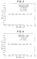
- the ratio of its power outputs from the two terminals was determined, and the power split ratio was plotted as a function of wavelength as seen in Fig. 3.
- the power split ratio for any wavelengths enclosed in the band width of 120 nm is in the range of 50 ⁇ 0.79%.
- the ambient temperature was changed to -10, 0, 10, 30, and 40°C, and the measurement as had been performed on the device kept at 20°C was repeated.
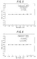
- the power split ratio of TE and TM polarization was plotted as a function of wavelength. The results are shown in Figs. 4, 5, 6, 7 and 8. As seen from the figures, the power split ratios are in the range of 50 ⁇ 0.71,50 ⁇ 0.73, 50 ⁇ 0.76, 50 ⁇ 0.81, and 50 ⁇ 0.84% respectively. They were hardly affected by the changes of polarization and ambient temperature and wavelength..
- the polymeric optical waveguide coupler circuit 8 of this invention stable to the changes of polarization and ambient temperature, optical signals falling within the bandwidth of 120 nm with 1550 nm at their central wavelength which are used in fiber optic communication based on dense wavelength division multiplexing are reliably routed because their wavelength being hardly modified during their passage through the circuit, even when the ambient temperature is changed from -10°C to 40°C. Accordingly, the polymeric optical waveguide coupler circuit 8 of this invention stable to the changes of polarization and ambient temperature may serve, as one of its applications, as thermally stable couplers 9 independent of polarization constituting a polymeric optical waveguide 2 ⁇ 2N splitter as shown in Fig. 2.
- the cross-sections and refractive indices of the waveguides and the parameters of other circuit elements constituting the polymeric optical waveguide coupler circuit device are optimized such that light passing through the device can reliably keep its wavelength unaffected by the changes of polarization and ambient temperature.
- the effect of the change of polarization and ambient temperature on the power split ratio of the device which would be otherwise manifest is obviously minimized.
- optical signals falling within a bandwidth of 120 nm with 1550 nm at its central wavelength which are used in fiber optic communication based on dense wavelength division multiplexing are reliably routed even when the ambient temperature is changed from -10°C to 40°C, without requiring a certain heat-insulating means, without requiring a certain polarization maintenance means.
- the optical waveguide circuit device of this invention is optimized as described above, even wavelengths are hardly affected by the change of polarization and ambient temperature, and characteristics dependent of wavelength, polarization and temperature, is suppressed to nearly Zero. Thus, it may be used, as one of its applications, as a thermally stable polymeric optical waveguide 2 ⁇ 2N splitter independent of polarization.
- the method provided by the present invention optimizes the optical waveguide coupling circuit device using the same materials as used in the conventional optical waveguide device, it is not necessary to alter the conventional fabrication processes themselves.
- the method of this invention maintaining the advantage of the conventional method of producing a polymeric optical waveguide device, that is, the low production cost, ensures the production of an optical waveguide circuit device stable to the changes of polarization and ambient temperature.
Landscapes
- Physics & Mathematics (AREA)
- Engineering & Computer Science (AREA)
- Microelectronics & Electronic Packaging (AREA)
- General Physics & Mathematics (AREA)
- Optics & Photonics (AREA)
- Optical Integrated Circuits (AREA)
Applications Claiming Priority (2)
| Application Number | Priority Date | Filing Date | Title |
|---|---|---|---|
| JP2002193818A JP3923383B2 (ja) | 2002-07-02 | 2002-07-02 | 光導波路カプラ回路デバイス |
| JP2002193818 | 2002-07-02 |
Publications (2)
| Publication Number | Publication Date |
|---|---|
| EP1378773A2 true EP1378773A2 (fr) | 2004-01-07 |
| EP1378773A3 EP1378773A3 (fr) | 2004-07-14 |
Family
ID=29720258
Family Applications (1)
| Application Number | Title | Priority Date | Filing Date |
|---|---|---|---|
| EP03254154A Withdrawn EP1378773A3 (fr) | 2002-07-02 | 2003-06-30 | Coupleur de guides d'ondes optiques |
Country Status (6)
| Country | Link |
|---|---|
| US (1) | US7027690B2 (fr) |
| EP (1) | EP1378773A3 (fr) |
| JP (1) | JP3923383B2 (fr) |
| KR (1) | KR100695602B1 (fr) |
| CN (1) | CN1320379C (fr) |
| TW (1) | TWI224690B (fr) |
Families Citing this family (17)
| Publication number | Priority date | Publication date | Assignee | Title |
|---|---|---|---|---|
| JP3802838B2 (ja) * | 2001-05-30 | 2006-07-26 | 古河電気工業株式会社 | 光合分波器 |
| JP3790177B2 (ja) * | 2002-03-07 | 2006-06-28 | ニッタ株式会社 | 光導波路カプラ回路デバイス |
| US6990283B2 (en) * | 2003-02-15 | 2006-01-24 | Electronics And Telecommnications Research Institute | Polymeric optical device having low polarization dependence and method of fabricating the same |
| US7519240B1 (en) * | 2007-07-17 | 2009-04-14 | Infinera Corporation | Multi-section coupler to mitigate guide-guide asymmetry |
| CN102323227B (zh) * | 2011-06-13 | 2013-12-25 | 上海理工大学 | 一种生物溶液浓度的光谱传感测试方法 |
| CN102354022B (zh) * | 2011-10-28 | 2013-05-22 | 武汉邮电科学研究院 | 基于纳米线波导的波长和偏振定向耦合器及其制造方法 |
| JP2013221996A (ja) * | 2012-04-13 | 2013-10-28 | Furukawa Electric Co Ltd:The | 広帯域動作光カプラ |
| CN108415123A (zh) * | 2013-02-18 | 2018-08-17 | 日本电气株式会社 | 偏振分束器和光器件 |
| JP6382195B2 (ja) * | 2013-07-10 | 2018-08-29 | 技術研究組合光電子融合基盤技術研究所 | 光回路 |
| JP6372142B2 (ja) * | 2014-04-11 | 2018-08-15 | 沖電気工業株式会社 | 光波長分波器 |
| CN103994783B (zh) * | 2014-05-23 | 2016-07-06 | 华中科技大学 | 一种基于集成光波导耦合器的波长解调装置 |
| US10248002B2 (en) * | 2015-03-30 | 2019-04-02 | Nec Corporation | Optical circuit, and optical switch using same |
| EP3824571A4 (fr) | 2018-07-17 | 2022-04-13 | CommScope Technologies LLC | Système de communication optique à fibres utilisant un diviseur de guide d'ondes optique asymétrique |
| WO2020103164A1 (fr) * | 2018-11-24 | 2020-05-28 | 华为技术有限公司 | Dispositif de traitement de polarisation, émetteur-récepteur optique, et procédé de traitement de polarisation optique |
| CN109407211B (zh) * | 2018-11-30 | 2021-03-02 | 武汉邮电科学研究院有限公司 | 一种波导元件及分合束器 |
| CN109343173B (zh) * | 2018-12-06 | 2023-08-25 | 安徽问天量子科技股份有限公司 | 一种混合波导集成的干涉仪 |
| JP7425544B2 (ja) * | 2019-05-13 | 2024-01-31 | 日東電工株式会社 | プラスチック光ファイバおよびその製造方法、ならびに該プラスチック光ファイバを用いたプラスチック光ファイバコード |
Family Cites Families (9)
| Publication number | Priority date | Publication date | Assignee | Title |
|---|---|---|---|---|
| JP2966113B2 (ja) * | 1990-12-27 | 1999-10-25 | 古河電気工業株式会社 | 導波路型分岐結合器 |
| US5247594A (en) * | 1991-03-22 | 1993-09-21 | Nippon Telegraph And Telephone Corporation | Waveguide-type optical matrix switch |
| DE4240266A1 (de) * | 1992-12-01 | 1994-06-09 | Bosch Gmbh Robert | Verfahren zur Herstellung optischer Polymerbauelemente mit integrierten vertikalen Koppelstrukturen |
| JP3022181B2 (ja) * | 1994-03-18 | 2000-03-15 | 日立電線株式会社 | 導波路型光合分波器 |
| EP0909403B1 (fr) * | 1996-07-26 | 2002-10-02 | STMicroelectronics S.r.l. | Dispositif optique ajustable d'insertion/extraction |
| JPH10227931A (ja) * | 1997-02-13 | 1998-08-25 | Nippon Telegr & Teleph Corp <Ntt> | 導波路型光デバイス |
| JP3027965B2 (ja) * | 1997-06-18 | 2000-04-04 | 日本電気株式会社 | 光合分波装置 |
| US6922507B2 (en) * | 2002-03-01 | 2005-07-26 | Lucent Technologies Inc. | Low-loss integrated optical coupler and optical switch |
| JP3790177B2 (ja) * | 2002-03-07 | 2006-06-28 | ニッタ株式会社 | 光導波路カプラ回路デバイス |
-
2002
- 2002-07-02 JP JP2002193818A patent/JP3923383B2/ja not_active Expired - Fee Related
-
2003
- 2003-06-20 TW TW092116785A patent/TWI224690B/zh not_active IP Right Cessation
- 2003-06-30 KR KR1020030043297A patent/KR100695602B1/ko not_active Expired - Fee Related
- 2003-06-30 EP EP03254154A patent/EP1378773A3/fr not_active Withdrawn
- 2003-07-02 US US10/610,590 patent/US7027690B2/en not_active Expired - Fee Related
- 2003-07-02 CN CNB031457614A patent/CN1320379C/zh not_active Expired - Fee Related
Also Published As
| Publication number | Publication date |
|---|---|
| US7027690B2 (en) | 2006-04-11 |
| TW200403456A (en) | 2004-03-01 |
| CN1320379C (zh) | 2007-06-06 |
| EP1378773A3 (fr) | 2004-07-14 |
| JP2004037769A (ja) | 2004-02-05 |
| TWI224690B (en) | 2004-12-01 |
| US20040067022A1 (en) | 2004-04-08 |
| KR20040004075A (ko) | 2004-01-13 |
| KR100695602B1 (ko) | 2007-03-14 |
| JP3923383B2 (ja) | 2007-05-30 |
| CN1475822A (zh) | 2004-02-18 |
Similar Documents
| Publication | Publication Date | Title |
|---|---|---|
| US7027690B2 (en) | Optical waveguide coupler circuit device | |
| EP1191364A1 (fr) | Interferometre optique a guide d'ondes | |
| US5940555A (en) | Optical multiplexer/demultiplexer | |
| US20050129363A1 (en) | Arrayed waveguide grating with waveguides of unequal widths | |
| US6731828B2 (en) | Waveguide-type optical signal processing circuit | |
| US6724957B2 (en) | Optical filter | |
| US6836598B2 (en) | Optical waveguide coupler circuit device | |
| US6631223B2 (en) | Optical multiplexer/demultiplexer | |
| US6539158B2 (en) | Optical waveguide circuit | |
| US6690852B2 (en) | Optical multiplexer/demultiplexer | |
| HK1059825A (en) | Optical waveguide coupler device | |
| KR20050097923A (ko) | 어레이 도파로 격자형 광 합/분파 회로 | |
| KR100487216B1 (ko) | 정렬성이 향상된 온도 무의존형 파장분할 다중화/역다중화장치 및 그 정렬방법 | |
| JP2005062756A (ja) | 光導波路カプラ回路デバイス | |
| JP2006047737A (ja) | 光導波路カプラ回路デバイス | |
| Roeloffzen et al. | Passband-flattened periodic multi/demultiplexer using a mach-zehnder interferometer with ring resonator fabricated in SiON waveguide technology | |
| JP2006267263A (ja) | 光導波路カプラ回路デバイス | |
| Mayeh et al. | Geometrically modified multimode interference waveguides using high refractive index SiON material, for application in wavelength multiplexing/demultiplexing | |
| JP2004109245A (ja) | 高分子光導波路インタリーバ回路デバイス |
Legal Events
| Date | Code | Title | Description |
|---|---|---|---|
| PUAI | Public reference made under article 153(3) epc to a published international application that has entered the european phase |
Free format text: ORIGINAL CODE: 0009012 |
|
| AK | Designated contracting states |
Kind code of ref document: A2 Designated state(s): AT BE BG CH CY CZ DE DK EE ES FI FR GB GR HU IE IT LI LU MC NL PT RO SE SI SK TR |
|
| AX | Request for extension of the european patent |
Extension state: AL LT LV MK |
|
| PUAL | Search report despatched |
Free format text: ORIGINAL CODE: 0009013 |
|
| 17P | Request for examination filed |
Effective date: 20040517 |
|
| AK | Designated contracting states |
Kind code of ref document: A3 Designated state(s): AT BE BG CH CY CZ DE DK EE ES FI FR GB GR HU IE IT LI LU MC NL PT RO SE SI SK TR |
|
| AX | Request for extension of the european patent |
Extension state: AL LT LV MK |
|
| REG | Reference to a national code |
Ref country code: HK Ref legal event code: DE Ref document number: 1059825 Country of ref document: HK |
|
| 17Q | First examination report despatched |
Effective date: 20050104 |
|
| AKX | Designation fees paid |
Designated state(s): CH DE FR GB IT LI SE |
|
| STAA | Information on the status of an ep patent application or granted ep patent |
Free format text: STATUS: THE APPLICATION IS DEEMED TO BE WITHDRAWN |
|
| 18D | Application deemed to be withdrawn |
Effective date: 20100105 |
|
| REG | Reference to a national code |
Ref country code: HK Ref legal event code: WD Ref document number: 1059825 Country of ref document: HK |