EP1380056B2 - Ensemble composant optoelectronique et procede de fabrication d'un ensemble composant optoelectronique - Google Patents
Ensemble composant optoelectronique et procede de fabrication d'un ensemble composant optoelectronique Download PDFInfo
- Publication number
- EP1380056B2 EP1380056B2 EP02732539.8A EP02732539A EP1380056B2 EP 1380056 B2 EP1380056 B2 EP 1380056B2 EP 02732539 A EP02732539 A EP 02732539A EP 1380056 B2 EP1380056 B2 EP 1380056B2
- Authority
- EP
- European Patent Office
- Prior art keywords
- optoelectronic component
- casting material
- dam
- carrier element
- casting
- Prior art date
- Legal status (The legal status is an assumption and is not a legal conclusion. Google has not performed a legal analysis and makes no representation as to the accuracy of the status listed.)
- Expired - Lifetime
Links
Images
Classifications
-
- H—ELECTRICITY
- H10—SEMICONDUCTOR DEVICES; ELECTRIC SOLID-STATE DEVICES NOT OTHERWISE PROVIDED FOR
- H10F—INORGANIC SEMICONDUCTOR DEVICES SENSITIVE TO INFRARED RADIATION, LIGHT, ELECTROMAGNETIC RADIATION OF SHORTER WAVELENGTH OR CORPUSCULAR RADIATION
- H10F77/00—Constructional details of devices covered by this subclass
- H10F77/50—Encapsulations or containers
-
- H—ELECTRICITY
- H10—SEMICONDUCTOR DEVICES; ELECTRIC SOLID-STATE DEVICES NOT OTHERWISE PROVIDED FOR
- H10F—INORGANIC SEMICONDUCTOR DEVICES SENSITIVE TO INFRARED RADIATION, LIGHT, ELECTROMAGNETIC RADIATION OF SHORTER WAVELENGTH OR CORPUSCULAR RADIATION
- H10F39/00—Integrated devices, or assemblies of multiple devices, comprising at least one element covered by group H10F30/00, e.g. radiation detectors comprising photodiode arrays
- H10F39/80—Constructional details of image sensors
- H10F39/804—Containers or encapsulations
-
- H—ELECTRICITY
- H10—SEMICONDUCTOR DEVICES; ELECTRIC SOLID-STATE DEVICES NOT OTHERWISE PROVIDED FOR
- H10W—GENERIC PACKAGES, INTERCONNECTIONS, CONNECTORS OR OTHER CONSTRUCTIONAL DETAILS OF DEVICES COVERED BY CLASS H10
- H10W72/00—Interconnections or connectors in packages
- H10W72/01—Manufacture or treatment
- H10W72/015—Manufacture or treatment of bond wires
- H10W72/01515—Forming coatings
-
- H—ELECTRICITY
- H10—SEMICONDUCTOR DEVICES; ELECTRIC SOLID-STATE DEVICES NOT OTHERWISE PROVIDED FOR
- H10W—GENERIC PACKAGES, INTERCONNECTIONS, CONNECTORS OR OTHER CONSTRUCTIONAL DETAILS OF DEVICES COVERED BY CLASS H10
- H10W72/00—Interconnections or connectors in packages
- H10W72/071—Connecting or disconnecting
- H10W72/075—Connecting or disconnecting of bond wires
-
- H—ELECTRICITY
- H10—SEMICONDUCTOR DEVICES; ELECTRIC SOLID-STATE DEVICES NOT OTHERWISE PROVIDED FOR
- H10W—GENERIC PACKAGES, INTERCONNECTIONS, CONNECTORS OR OTHER CONSTRUCTIONAL DETAILS OF DEVICES COVERED BY CLASS H10
- H10W72/00—Interconnections or connectors in packages
- H10W72/50—Bond wires
- H10W72/551—Materials of bond wires
- H10W72/552—Materials of bond wires comprising metals or metalloids, e.g. silver
- H10W72/5522—Materials of bond wires comprising metals or metalloids, e.g. silver comprising gold [Au]
-
- H—ELECTRICITY
- H10—SEMICONDUCTOR DEVICES; ELECTRIC SOLID-STATE DEVICES NOT OTHERWISE PROVIDED FOR
- H10W—GENERIC PACKAGES, INTERCONNECTIONS, CONNECTORS OR OTHER CONSTRUCTIONAL DETAILS OF DEVICES COVERED BY CLASS H10
- H10W72/00—Interconnections or connectors in packages
- H10W72/50—Bond wires
- H10W72/551—Materials of bond wires
- H10W72/552—Materials of bond wires comprising metals or metalloids, e.g. silver
- H10W72/5524—Materials of bond wires comprising metals or metalloids, e.g. silver comprising aluminium [Al]
-
- H—ELECTRICITY
- H10—SEMICONDUCTOR DEVICES; ELECTRIC SOLID-STATE DEVICES NOT OTHERWISE PROVIDED FOR
- H10W—GENERIC PACKAGES, INTERCONNECTIONS, CONNECTORS OR OTHER CONSTRUCTIONAL DETAILS OF DEVICES COVERED BY CLASS H10
- H10W72/00—Interconnections or connectors in packages
- H10W72/50—Bond wires
- H10W72/551—Materials of bond wires
- H10W72/552—Materials of bond wires comprising metals or metalloids, e.g. silver
- H10W72/5525—Materials of bond wires comprising metals or metalloids, e.g. silver comprising copper [Cu]
-
- H—ELECTRICITY
- H10—SEMICONDUCTOR DEVICES; ELECTRIC SOLID-STATE DEVICES NOT OTHERWISE PROVIDED FOR
- H10W—GENERIC PACKAGES, INTERCONNECTIONS, CONNECTORS OR OTHER CONSTRUCTIONAL DETAILS OF DEVICES COVERED BY CLASS H10
- H10W74/00—Encapsulations, e.g. protective coatings
-
- H—ELECTRICITY
- H10—SEMICONDUCTOR DEVICES; ELECTRIC SOLID-STATE DEVICES NOT OTHERWISE PROVIDED FOR
- H10W—GENERIC PACKAGES, INTERCONNECTIONS, CONNECTORS OR OTHER CONSTRUCTIONAL DETAILS OF DEVICES COVERED BY CLASS H10
- H10W90/00—Package configurations
- H10W90/701—Package configurations characterised by the relative positions of pads or connectors relative to package parts
- H10W90/751—Package configurations characterised by the relative positions of pads or connectors relative to package parts of bond wires
- H10W90/754—Package configurations characterised by the relative positions of pads or connectors relative to package parts of bond wires between a chip and a stacked insulating package substrate, interposer or RDL
Definitions
- the present invention relates to an optoelectronic component arrangement. Furthermore, the present invention relates to a method for producing an optoelectronic component arrangement.
- An optoelectronic component arrangement is known from JP 8-241976.
- a carrier element designed as a CCD chip optoelectronic device is arranged, which is surrounded by a ring-shaped dam.
- the device is connected via bonding wires with lines in the carrier element and is contacted so electrically.
- a potting is arranged, which consists of two transparent potting materials. Due to thermally induced stresses cracks can occur in the encapsulation and possibly damage the bonding wires. It is therefore proposed to introduce in a first step, a first transparent potting material in the dam interior, this thermally curing and thereby eliminate air bubbles from the potting material.
- a second transparent potting compound is introduced into the dam interior and in turn thermally cured in order to eliminate any air bubbles in the second potting material. In this way it can be ensured that no more air bubbles are contained in the two potting materials. If materials with greatly differing thermal expansion coefficients are now used in such a component arrangement, bond wire cracks can occur under thermal loads. Significantly different thermal expansion coefficients have, for example, the transparent casting materials or epoxy resins used on the one hand ( ⁇ 50-70 ppm / K) and, on the other hand, the materials used for the carrier element or bonding wires ( ⁇ 15-25 ppm / K).
- US Pat. No. 5,861,680 discloses various optoelectronic component arrangements in which an optoelectrical component is in each case surrounded by a dam or frame on a carrier element, wherein the component is electrically contacted via bonding wires.
- the interior of the dam or frame is filled with a transparent potting material.
- Figs. 1A and 1B differ only in the arrangement of e.g. on a board or by the respective contacting possibility;
- Fig. 1A discloses a so-called DIP arrangement which is suitable for push-through mounting
- Fig. 1B an LCC arrangement is shown, which is suitable for SMD assembly.
- a temperature-induced damage to the bonding wires to be prevented in accordance with this document that the hardness of the potting material is adjusted during manufacture suitable.
- a photodetector arrangement with a multilayer filter and a method for its production are known.
- a photodetector element is placed in a depression of a carrier element, which is contacted by means of bonding wires.
- a first non-transparent potting material is disposed adjacent to the photodetector element, above a second transparent potting material.
- a disadvantage of this arrangement is in particular that a complex shaping processing of the support member is necessary to form the depression.
- the object of the present invention is therefore to specify an optoelectronic component arrangement and a suitable method for the production thereof, which ensures that the bonding wires provided for contacting the optoelectronic component are not damaged even at varying temperatures.
- the second stated object is achieved by a method for producing an optoelectronic component arrangement according to the measures of claim 9.
- a first potting material is now introduced into the inner area of the dam, with the first potting material advantageously extending to the upper edge of the optoelectronic component. At least in a spatially defined window area a transparent second potting material is introduced over it.
- the first potting material is preferably chosen differently, to the transparent second potting material. In particular, in the choice of the first potting material is taken into account that this has the lowest possible thermal expansion coefficient, which is adapted to the thermal expansion coefficient of the bonding wires used and the carrier element used. In this way and
- a particular manufacturing advantage results in a possible embodiment of the method according to the invention, when the first potting material and the dam material consist of the substantially same base material and only have different viscosities, since then the first potting material and the dam are applied and cured in the same step can.
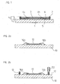
- FIG. 1 is a schematic side sectional view of a first embodiment of the optoelectronic component assembly according to the invention shown.
- the support element 1 is formed in this example as a known circuit board made of FR4 material. Alternatively, however, other materials for the support element 1 into consideration, such as FR5, alumina, glass, etc. ..
- an unhoused component 3 is provided in the illustrated embodiment in the form of a photodetector whose radiation-sensitive surface is oriented away from the carrier element 1.
- a corresponding unhoused light source a so-called.
- Opto-ASIC or other optoelectronic element as optoelectronic device 3 could be used at this point.
- the respective optoelectronic component 3 is connected by means of bonding wires 4a, 4b to the electrical lines in the carrier element 1 or electrically contacted via the bonding wires 4a, 4b in a known manner.
- the material used for the bonding wires 4a, 4b in the present example is gold.
- gold alloys, aluminum, aluminum alloys or copper can be used as bonding wire materials.
- the optoelectronic component 2 is glued in the illustrated embodiment on the Queen element 1; Alternatively, this compound could also be made by alloying, eutectic bonding, anodized bonding, brazing or welding.
- the optoelectronic component arrangement according to the invention comprises a dam 2 arranged on the carrier element 1, which surrounds or circumscribes the component 3 in a closed manner.
- the dam 2 can have a variety of Umlaufgeometrien;
- the dam 2 may surround the structural element 3 in a square manner, but alternatively it is also possible for a rectangular, polygonal or circular embankment course to be provided around the structural element 3.
- the dam 2 has a height h 2 , which is chosen significantly larger than the height h 1 of the component 3 in the present example.
- An essential function of the dam 2 in the device arrangement according to the invention is that it limits the required area on the carrier element 1, which is required for potting the component 3 in the inner area of the dam with encapsulation.
- two potting materials 5, 6 are used for potting, as will be explained in detail below.
- the casting of the component arrangement with the two potting materials 5, 6 serves to protect the component 3 and the bonding wires 4a, 4b against mechanical influences.
- a known black Epoxy galllmasse be provided in the form of a filled epoxy resin, as sold by the company Emerson & Cuming under the type name Amicon 50300 HT .
- epoxy fillers from Dexter Hysol , which are sold under the product designations FP 4451 .
- the dam 2 consists in the present embodiment of a single dam layer, as shown in FIG. 1 is apparent.
- a two- or multi-layer dam structure could also be provided, as described, for example, in German Patent Application No. 100 24 336.3.
- the encapsulation which encapsulates the optoelectronic component 3, arranged in the trough-like dam interior, consists of two different encapsulation materials 5, 6.
- the inner dam area is filled up to the upper edge of the optoelectronic component 3 with a first potting material 5.
- the first potting material 5 in the example shown has a height that corresponds to the height h 1 of the component 3.
- the perineal area is filled up to the upper edge of the optoelectronic component 3 with the first potting material and consequently that the radiation-sensitive or optionally radiation-emitting surface of the optoelectronic component 3 is not substantially covered by the first potting material 5.
- the first potting material 5 is selected such that its thermal expansion coefficient ⁇ VM1 is matched to the thermal expansion coefficients of the bonding wires 4a, 4b ( ⁇ BD ) and of the carrier element 1 ( ⁇ TE ).
- a black Epoxy galmasse is used, which has a thermal expansion coefficient ⁇ VM1 ⁇ 18-19 ppm / K. This is compared to the thermal expansion coefficient ⁇ BD ⁇ 15 ppm / K of the bonding wires 4a, 4b already achieved a very good match when gold is used as the material for the bonding wires 4a, 4b.
- the other materials already mentioned above for the bonding wires 4a, 4b also have coefficients of thermal expansion in the range of .alpha. BD.sup. + (15 ppm / K-25 ppm / K).
- FR4 as the material for the carrier element 1
- Suitable first potting materials 5 are sold for example by the company Emerson & Cuming or Dexter Hysol under the product name Amicon 50500-1 or FP 4450.
- the first potting material 5 and the material of the dam 2 therefore have the same base material in the illustrated embodiment and have only different viscosities. As will be explained later, this choice of material also results in advantages in the course of a possible embodiment of the production method according to the invention.
- the first potting material 5 is further selected such that it has the largest possible surface roughness in the cured state. As a result, a very good adhesion with the overlying material, namely the second potting material 6 can be ensured.
- the second potting material 6 is a commercially available transparent potting material, which is arranged in the dam interior area at least in a window area above the optoelectronic component 3, that is, for example, in the radiation-sensitive region of the photoelement etc. Suitable for the second potting material 6, for example the product marketed by Dexter Hysol under the product name Hysol OS 2800 . Alternatively, the potting materials sold under the product names Hysol OS 1600, Hysol OS 1900, Hysol OS 2902, Hysol OS 4000 or Hysol OS 4110 by the same company would also be usable at this point.
- the second potting material 6 completely fills the dam interior area above the first potting material 5 and the optoelectronic component 3. As already mentioned, however, alternatively only a smaller window area could be filled with it.
- the arrangement according to the invention and the choice of potting materials 5, 6 ensure that the total filling volume in the interior of the dam, which must be filled with the transparent second potting material 6, can be significantly reduced.
- the problems in connection with the thermally induced shearing off of the bonding wires 4a, 4b resulted mainly due to the strongly differing thermal expansion coefficients of transparent potting materials on the one hand and the bonding wires 4a, 4b or of the carrier element 1 on the other hand.
- the reduced fill volume also has the positive effect of reducing the stresses within the device arrangement due to the curing shrinkage process.
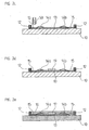
- the unpackaged optoelectronic component 13 is first arranged in the form of an opto-ASIC on the carrier element 10 or the printed circuit board and glued thereto. Furthermore, the optoelectronic component 13 is electrically contacted, which can be done in a known manner via wire bonding and the arrangement of corresponding bonding wires 14a, 14b.
- the dam 12 is applied to the carrier element 10 with the height h 2 , which, as explained above, completely encloses the optoelectronic component 13.
- the corresponding process step is in FIG. 2b illustrated.
- the application of the corresponding dam material is carried out in this example by means of a schematically indicated dispensing needle 50 in the so-called. Dispense technique.
- a dam or frame element designed as an injection molded part could be placed on the carrier element.
- the desired height h 2 of the dam 12 can be defined in the case of application via the dispensing technique by adjusting the speed of the dispensing needle 50, the applied amount of dam material, etc. defined.
- a first potting material 15 is introduced in the dam interior area with the aid of the dispensing needle 50 up to the height h 1 of the component upper edge.
- a first potting material 15 is selected, which consists of the same base material as the dam 12.
- a black, filled epoxy resin or an epoxy filling compound can be used for this purpose.
- the curing of the dam 12 and of the first potting material 15 takes place via a suitable tempering process.
- an additional glass plate 19 is arranged on the radiation-sensitive surface of the component 13 or of the opto-ASIC. This can be like in Figure 2d indicated before filling with the second transparent potting material; Alternatively, however, it is also possible to press the glass plate 19 onto the surface of the component 13 only after the rest of the inner wall of the dam has been filled with the transparent second potting material.
- the arrangement of the glass plate 19 is used in the case of devices 13 with non-passivated active surfaces to protect or seal these surfaces.
- the thickness of the glass plate 19 is selected to be large enough, an additional mechanical protection for the bonding wires 14a, 14b can be ensured.
- the glass plate may of course also have a greater thickness and then slightly protrude from the second potting material.
- the remaining inner dam area is filled by means of the dispensing needle 70 with the second potting material 16 to about the dam top edge, for which, as explained above, a transparent potting material is used.
Landscapes
- Structures Or Materials For Encapsulating Or Coating Semiconductor Devices Or Solid State Devices (AREA)
- Led Device Packages (AREA)
- Solid State Image Pick-Up Elements (AREA)
- Light Receiving Elements (AREA)
- Photovoltaic Devices (AREA)
Claims (14)
- Ensemble à composant optoélectronique, constitué- d'un élément support (1 ; 10) ;- d'un composant optoélectronique (3 ; 13) qui est disposé sur l'élément support (1 ; 10) et est connecté par des fils de liaison (4a, 4b ; 14a, 14b) à des conducteurs situés dans l'élément support (1 ; 10),- d'une barrière (2 ; 12) fermée qui est disposée sur l'élément support (1 ; 10) et entoure le composant optoélectronique (3 ; 13),- d'une masse de scellement, disposée dans la zone intérieure de la barrière, qui enveloppe le composant optoélectronique (3 ; 13) et comprend deux matériaux de scellement (5, 6 ; 15, 16),- la zone intérieure de la barrière qui est située au-dessus du composant optoélectronique (3 ; 13) étant remplie avec un deuxième matériau de scellement (6 ; 16) transparent, au moins dans une zone de fenêtre, et- la zone intérieure de la barrière étant remplie avec un premier matériau de scellement (5 ; 15) non transparent, jusqu'au bord supérieur du composant optoélectronique (3 ; 13), et- les fils de liaison (4a, 4b ; 14a, 14b) étant entourés par le premier matériau de scellement (5 ; 15) au niveau de leur extrémité du côté de l'élément support et- le premier matériau de scellement (5 ; 15) présentant un coefficient de dilatation thermique (αVM1) qui est adapté au coefficient de dilatation thermique (αBD) des fils de liaison (4a, 4b ; 14a, 14b) et au coefficient de dilatation thermique (αTE) de l'élément support (1 ; 10).
- Ensemble à composant optoélectronique selon la revendication 1, dans lequel le premier matériau de scellement (5 ; 15) présente un coefficient de dilatation thermique αVM1 ≈ 18-19 ppm/K.
- Ensemble à composant optoélectronique selon la revendication 1, dans lequel à l'état durci, le premier matériau de scellement (5 ; 15) présente une rugosité de surface élevée.
- Ensemble à composant optoélectronique selon la revendication 1, dans lequel le premier matériau de scellement (5 ; 15) est une masse de remplissage époxy noire.
- Ensemble à composant optoélectronique selon la revendication 1, dans lequel le premier matériau de scellement (5 ; 15) et le matériau de la barrière (2 ; 12) sont faits du même matériau de base et présentent seulement des viscosités différentes.
- Ensemble à composant optoélectronique selon la revendication 1, dans lequel le deuxième matériau de scellement (6 ; 16) remplit complètement la zone intérieure de la barrière, au-dessus du premier matériau de scellement (5 ; 15) et du composant optoélectronique (3 ; 13).
- Ensemble à composant optoélectronique selon la revendication 1, dans lequel le composant optoélectronique (3 ; 13) est réalisé sous forme de cellule photoélectrique ou de circuit optoélectronique ASIC, dont la surface sensible au rayonnement est orientée dans la direction opposée à l'élément support (1 ; 10) .
- Ensemble à composant optoélectronique selon la revendication 7, dans lequel une plaque de verre (19) est disposée directement sur la surface sensiblement au rayonnement de la cellule photoélectrique ou du circuit optoélectronique ASIC.
- Procédé de fabrication d'un ensemble à composant optoélectronique, dans lequel- un composant optoélectronique (3 ; 13) est d'abord disposé sur un élément support (1 ; 10) et est mis en contact électrique par le biais de fils de liaison (4a, 4b ; 14a, 14b),- ensuite, une barrière (2 ; 12) fermée est introduite sur l'élément support (1 ; 10), autour du composant optoélectronique (3 ; 13), et- une masse de scellement, constituée de deux matériaux de scellement (5, 6 ; 15 ; 16), est introduite dans la zone intérieure de la barrière pour envelopper le composant optoélectronique (3 ; 13),- la zone intérieure de la barrière qui est située au-dessus du composant optoélectronique (3 ; 13) étant remplie avec un deuxième matériau de scellement (6 ; 16) transparent, au moins dans une zone de fenêtre, et- pour la mise en place de la masse de scellement, un premier matériau de scellement (5 ; 15) non transparent étant d'abord introduit dans la zone intérieure de la barrière, jusqu'au bord supérieur du composant optoélectronique (3 ; 13), de sorte que les fils de liaison (4a, 4b ; 14a, 14b) soient entourés au niveau de leur extrémité du côté de l'élément support par le premier matériau de scellement (5 ; 15) et- un premier matériau de scellement (5 ; 15) présentant un coefficient de dilatation thermique (αVM1) qui est adapté au coefficient de dilatation thermique (αBD) des fils de liaison (4a, 4b ; 14a, 14b) et au coefficient de dilatation thermique (αTE) de l'élément support (1 ; 10) étant choisi.
- Procédé selon la revendication 9, dans lequel un premier matériau de scellement (5 ; 15) est choisi, lequel présente un coefficient de dilatation thermique αVM1 ≈ 18 - 19 ppm/K.
- Procédé selon la revendication 9, dans lequel un premier matériau de scellement (5 ; 15) est choisi, lequel présente une rugosité de surface élevée à l'état durci.
- Procédé selon la revendication 9, dans lequel une masse de remplissage époxy noire est choisie en tant que premier matériau de scellement (5 ; 15).
- Procédé selon la revendication 9, dans lequel le deuxième matériau de scellement (6 ; 16) est introduit dans toute la zone intérieure de la barrière au-dessus du premier matériau de scellement (5 ; 15).
- Procédé selon la revendication 9, dans lequel le composant optoélectronique (3 ; 13) est connecté de manière électriquement conductrice à des pistes conductrices situées dans l'élément support (1 ; 10).
Applications Claiming Priority (3)
| Application Number | Priority Date | Filing Date | Title |
|---|---|---|---|
| DE10118231A DE10118231A1 (de) | 2001-04-11 | 2001-04-11 | Optoelektronische Baulelmentanordnung und Verfahren zur Herstellun einer oploelektronischen Bauelementanordnung |
| DE10118231 | 2001-04-11 | ||
| PCT/EP2002/003564 WO2002084746A2 (fr) | 2001-04-11 | 2002-03-30 | Ensemble composant optoelectronique et procede de fabrication d'un ensemble composant optoelectronique |
Publications (3)
| Publication Number | Publication Date |
|---|---|
| EP1380056A2 EP1380056A2 (fr) | 2004-01-14 |
| EP1380056B1 EP1380056B1 (fr) | 2007-05-23 |
| EP1380056B2 true EP1380056B2 (fr) | 2014-07-09 |
Family
ID=7681320
Family Applications (1)
| Application Number | Title | Priority Date | Filing Date |
|---|---|---|---|
| EP02732539.8A Expired - Lifetime EP1380056B2 (fr) | 2001-04-11 | 2002-03-30 | Ensemble composant optoelectronique et procede de fabrication d'un ensemble composant optoelectronique |
Country Status (6)
| Country | Link |
|---|---|
| US (1) | US6861683B2 (fr) |
| EP (1) | EP1380056B2 (fr) |
| JP (1) | JP4369127B2 (fr) |
| AT (1) | ATE363132T1 (fr) |
| DE (2) | DE10118231A1 (fr) |
| WO (1) | WO2002084746A2 (fr) |
Families Citing this family (40)
| Publication number | Priority date | Publication date | Assignee | Title |
|---|---|---|---|---|
| US7170188B2 (en) * | 2004-06-30 | 2007-01-30 | Intel Corporation | Package stress management |
| US7161345B2 (en) * | 2004-09-09 | 2007-01-09 | Veris Industries, Llc | Power monitoring system that determines phase using a superimposed signal |
| US7273767B2 (en) * | 2004-12-31 | 2007-09-25 | Carsem (M) Sdn. Bhd. | Method of manufacturing a cavity package |
| US7364945B2 (en) | 2005-03-31 | 2008-04-29 | Stats Chippac Ltd. | Method of mounting an integrated circuit package in an encapsulant cavity |
| US7354800B2 (en) * | 2005-04-29 | 2008-04-08 | Stats Chippac Ltd. | Method of fabricating a stacked integrated circuit package system |
| DE102005021991A1 (de) | 2005-05-09 | 2006-11-16 | Dr. Johannes Heidenhain Gmbh | Optoelektronische Anordnung und Verfahren zu deren Herstellung |
| US7663214B2 (en) * | 2005-07-25 | 2010-02-16 | Kingston Technology Corporation | High-capacity memory card and method of making the same |
| WO2007012992A1 (fr) * | 2005-07-28 | 2007-02-01 | Nxp B.V. | Emballage et procede de fabrication pour un composant microelectronique |
| US7723146B2 (en) * | 2006-01-04 | 2010-05-25 | Stats Chippac Ltd. | Integrated circuit package system with image sensor system |
| US7456088B2 (en) | 2006-01-04 | 2008-11-25 | Stats Chippac Ltd. | Integrated circuit package system including stacked die |
| US7768125B2 (en) | 2006-01-04 | 2010-08-03 | Stats Chippac Ltd. | Multi-chip package system |
| US7750482B2 (en) | 2006-02-09 | 2010-07-06 | Stats Chippac Ltd. | Integrated circuit package system including zero fillet resin |
| US8704349B2 (en) | 2006-02-14 | 2014-04-22 | Stats Chippac Ltd. | Integrated circuit package system with exposed interconnects |
| RU2308788C1 (ru) * | 2006-03-31 | 2007-10-20 | Федеральное государственное унитарное предприятие "НПО "ОРИОН" ФГУП "НПО "ОРИОН" | Способ сборки фотоприемников на основе сернистого свинца с применением метода полимерной герметизации |
| US20080122122A1 (en) * | 2006-11-08 | 2008-05-29 | Weng Fei Wong | Semiconductor package with encapsulant delamination-reducing structure and method of making the package |
| CA2609619A1 (fr) | 2007-09-10 | 2009-03-10 | Veris Industries, Llc | Indicateur d'etat |
| CA2609611A1 (fr) * | 2007-09-10 | 2009-03-10 | Veris Industries, Llc | Indicateur d'etat a noyaux de bobinage segmentes |
| CA2609629A1 (fr) * | 2007-09-10 | 2009-03-10 | Veris Industries, Llc | Commande electrique de courant avec etalonnage automatique |
| US8212548B2 (en) | 2008-06-02 | 2012-07-03 | Veris Industries, Llc | Branch meter with configurable sensor strip arrangement |
| US8421443B2 (en) | 2008-11-21 | 2013-04-16 | Veris Industries, Llc | Branch current monitor with calibration |
| US8421639B2 (en) | 2008-11-21 | 2013-04-16 | Veris Industries, Llc | Branch current monitor with an alarm |
| US9335352B2 (en) * | 2009-03-13 | 2016-05-10 | Veris Industries, Llc | Branch circuit monitor power measurement |
| US10006948B2 (en) | 2011-02-25 | 2018-06-26 | Veris Industries, Llc | Current meter with voltage awareness |
| US9146264B2 (en) | 2011-02-25 | 2015-09-29 | Veris Industries, Llc | Current meter with on board memory |
| US9329996B2 (en) | 2011-04-27 | 2016-05-03 | Veris Industries, Llc | Branch circuit monitor with paging register |
| US9250308B2 (en) | 2011-06-03 | 2016-02-02 | Veris Industries, Llc | Simplified energy meter configuration |
| US9410552B2 (en) | 2011-10-05 | 2016-08-09 | Veris Industries, Llc | Current switch with automatic calibration |
| CN102931178A (zh) * | 2012-07-30 | 2013-02-13 | 易美芯光(北京)科技有限公司 | 一种新型led集成光源封装结构 |
| US10242969B2 (en) * | 2013-11-12 | 2019-03-26 | Infineon Technologies Ag | Semiconductor package comprising a transistor chip module and a driver chip module and a method for fabricating the same |
| US9196510B2 (en) | 2013-11-12 | 2015-11-24 | Infineon Technologies Ag | Semiconductor package comprising two semiconductor modules and laterally extending connectors |
| US10274572B2 (en) | 2015-12-28 | 2019-04-30 | Veris Industries, Llc | Calibration system for a power meter |
| US10408911B2 (en) | 2015-12-28 | 2019-09-10 | Veris Industries, Llc | Network configurable system for a power meter |
| US10371721B2 (en) | 2015-12-28 | 2019-08-06 | Veris Industries, Llc | Configuration system for a power meter |
| US10371730B2 (en) | 2015-12-28 | 2019-08-06 | Veris Industries, Llc | Branch current monitor with client level access |
| KR20190030702A (ko) * | 2016-07-08 | 2019-03-22 | 스미또모 가가꾸 가부시키가이샤 | 자외선 발광 반도체 장치 및 그 제조 방법 |
| US11215650B2 (en) | 2017-02-28 | 2022-01-04 | Veris Industries, Llc | Phase aligned branch energy meter |
| US11193958B2 (en) | 2017-03-03 | 2021-12-07 | Veris Industries, Llc | Non-contact voltage sensor |
| US10705126B2 (en) | 2017-05-19 | 2020-07-07 | Veris Industries, Llc | Energy metering with temperature monitoring |
| CN111758168B (zh) * | 2018-02-19 | 2024-05-17 | 昕诺飞控股有限公司 | 具有光引擎的经密封的设备 |
| CN111176480A (zh) * | 2019-12-06 | 2020-05-19 | 深圳市鸿合创新信息技术有限责任公司 | 一种触控显示屏及其制备方法、触控装置 |
Family Cites Families (11)
| Publication number | Priority date | Publication date | Assignee | Title |
|---|---|---|---|---|
| JPS5834681A (ja) | 1981-08-26 | 1983-03-01 | Hitachi Ltd | 固体撮像装置 |
| DE3732075A1 (de) * | 1987-09-23 | 1989-04-06 | Siemens Ag | Hermetisch dichtes glas-metallgehaeuse fuer halbleiterbauelemente und verfahren zu dessen herstellung |
| JP3242495B2 (ja) | 1993-07-01 | 2001-12-25 | シャープ株式会社 | 多層膜フィルタ付き受光素子及びその製造方法 |
| JP3168859B2 (ja) | 1995-03-06 | 2001-05-21 | 日本ケミコン株式会社 | Ccdモジュールの樹脂封止方法 |
| DE19509262C2 (de) * | 1995-03-15 | 2001-11-29 | Siemens Ag | Halbleiterbauelement mit Kunststoffumhüllung und Verfahren zu dessen Herstellung |
| US5962810A (en) * | 1997-09-09 | 1999-10-05 | Amkor Technology, Inc. | Integrated circuit package employing a transparent encapsulant |
| DE19755734A1 (de) * | 1997-12-15 | 1999-06-24 | Siemens Ag | Verfahren zur Herstellung eines oberflächenmontierbaren optoelektronischen Bauelementes |
| DE19803936A1 (de) * | 1998-01-30 | 1999-08-05 | Patent Treuhand Ges Fuer Elektrische Gluehlampen Mbh | Ausdehnungskompensiertes optoelektronisches Halbleiter-Bauelement, insbesondere UV-emittierende Leuchtdiode und Verfahren zu seiner Herstellung |
| DE19947044B9 (de) * | 1999-09-30 | 2007-09-13 | Osram Opto Semiconductors Gmbh | Oberflächenmontierbares optoelektronisches Bauelement mit Reflektor und Verfahren zur Herstellung desselben |
| DE10023353A1 (de) | 2000-05-12 | 2001-11-29 | Osram Opto Semiconductors Gmbh | Optoelektronisches Bauelement und Verfahren zur Herstellung |
| DE10024336A1 (de) | 2000-05-17 | 2001-11-22 | Heidenhain Gmbh Dr Johannes | Bauelementanordnung und Verfahren zur Herstellung einer Bauelementanordnung |
-
2001
- 2001-04-11 DE DE10118231A patent/DE10118231A1/de not_active Withdrawn
-
2002
- 2002-03-30 WO PCT/EP2002/003564 patent/WO2002084746A2/fr not_active Ceased
- 2002-03-30 US US10/474,953 patent/US6861683B2/en not_active Expired - Fee Related
- 2002-03-30 DE DE50210203T patent/DE50210203D1/de not_active Expired - Lifetime
- 2002-03-30 JP JP2002581589A patent/JP4369127B2/ja not_active Expired - Fee Related
- 2002-03-30 AT AT02732539T patent/ATE363132T1/de not_active IP Right Cessation
- 2002-03-30 EP EP02732539.8A patent/EP1380056B2/fr not_active Expired - Lifetime
Also Published As
| Publication number | Publication date |
|---|---|
| JP2004528713A (ja) | 2004-09-16 |
| JP4369127B2 (ja) | 2009-11-18 |
| DE10118231A1 (de) | 2002-10-17 |
| WO2002084746A2 (fr) | 2002-10-24 |
| WO2002084746A3 (fr) | 2003-10-30 |
| US20040150064A1 (en) | 2004-08-05 |
| US6861683B2 (en) | 2005-03-01 |
| EP1380056A2 (fr) | 2004-01-14 |
| ATE363132T1 (de) | 2007-06-15 |
| DE50210203D1 (de) | 2007-07-05 |
| EP1380056B1 (fr) | 2007-05-23 |
Similar Documents
| Publication | Publication Date | Title |
|---|---|---|
| EP1380056B2 (fr) | Ensemble composant optoelectronique et procede de fabrication d'un ensemble composant optoelectronique | |
| EP1547166B1 (fr) | Module de sources de lumiere et procede de fabrication | |
| EP1022787B1 (fr) | Procédé de production d'un élément optique fixable sur une surface et élément optique fixable sur une surface | |
| EP0809304B1 (fr) | Convertisseur optoélectronique et procédé de fabrication | |
| DE19518753B4 (de) | Halbleitervorrichtung und Verfahren zu ihrer Herstellung | |
| DE69408549T2 (de) | Gehäuse für ein Halbleiterbauelement | |
| DE19921109B4 (de) | Elektronikbauteil und Elektronikkomponente mit einem Keramikbauteilelement | |
| EP1269450B1 (fr) | Composant pourvu d'une inscription | |
| DE3937996A1 (de) | Verfahren zur herstellung von halbleiteranordnungen | |
| EP1287558B1 (fr) | Ensemble de composants et son procede de fabrication | |
| EP1602625A1 (fr) | Module à semiconducteur avec un capteur à semiconducteur et un empaquetage en plastique et son procédé de fabrication. | |
| DE102009001969A1 (de) | Sensormodul | |
| DE3810899C2 (fr) | ||
| WO2008009262A2 (fr) | Module présentant une structure plate, et procédé permettant de l'équiper | |
| DE102005034011B4 (de) | Halbleiterbauteil für Hochfrequenzen über 10 GHz und Verfahren zur Herstellung desselben | |
| EP1717871B1 (fr) | Composant optoélectronique montable en surface | |
| DE112022002802B4 (de) | Halbleiterbauelement und verfahren zur herstellung eines halbleiterbauelements | |
| EP0243637B1 (fr) | Module de puissance à semi-conducteur | |
| DE102019127007A1 (de) | Stapel elektrischer bauelemente und verfahren zur herstellung desselben | |
| EP2260511B1 (fr) | Agencement de composants et procédé de fabrication d un agencement de composants | |
| WO2023036975A1 (fr) | Dispositif optoélectronique et procédé de production correspondant | |
| DE102014116080A1 (de) | Optoelektronisches Bauelement und Verfahren zu seiner Herstellung | |
| EP1466364B1 (fr) | Flan pour composants electroniques et procédé pour sa fabrication | |
| DE10014299B4 (de) | Chipverbund und Verfahren zu dessen Herstellung | |
| WO1998032172A1 (fr) | Composant electronique |
Legal Events
| Date | Code | Title | Description |
|---|---|---|---|
| PUAI | Public reference made under article 153(3) epc to a published international application that has entered the european phase |
Free format text: ORIGINAL CODE: 0009012 |
|
| AK | Designated contracting states |
Kind code of ref document: A2 Designated state(s): AT BE CH CY DE DK ES FI FR GB GR IE IT LI LU MC NL PT SE TR |
|
| 17P | Request for examination filed |
Effective date: 20040503 |
|
| 17Q | First examination report despatched |
Effective date: 20061002 |
|
| GRAP | Despatch of communication of intention to grant a patent |
Free format text: ORIGINAL CODE: EPIDOSNIGR1 |
|
| GRAS | Grant fee paid |
Free format text: ORIGINAL CODE: EPIDOSNIGR3 |
|
| GRAA | (expected) grant |
Free format text: ORIGINAL CODE: 0009210 |
|
| AK | Designated contracting states |
Kind code of ref document: B1 Designated state(s): AT BE CH CY DE DK ES FI FR GB GR IE IT LI LU MC NL PT SE TR |
|
| PG25 | Lapsed in a contracting state [announced via postgrant information from national office to epo] |
Ref country code: FI Free format text: LAPSE BECAUSE OF FAILURE TO SUBMIT A TRANSLATION OF THE DESCRIPTION OR TO PAY THE FEE WITHIN THE PRESCRIBED TIME-LIMIT Effective date: 20070523 |
|
| REG | Reference to a national code |
Ref country code: GB Ref legal event code: FG4D Free format text: NOT ENGLISH |
|
| GBT | Gb: translation of ep patent filed (gb section 77(6)(a)/1977) |
Effective date: 20070523 |
|
| REG | Reference to a national code |
Ref country code: CH Ref legal event code: EP |
|
| REG | Reference to a national code |
Ref country code: IE Ref legal event code: FG4D Free format text: LANGUAGE OF EP DOCUMENT: GERMAN |
|
| REF | Corresponds to: |
Ref document number: 50210203 Country of ref document: DE Date of ref document: 20070705 Kind code of ref document: P |
|
| PG25 | Lapsed in a contracting state [announced via postgrant information from national office to epo] |
Ref country code: SE Free format text: LAPSE BECAUSE OF FAILURE TO SUBMIT A TRANSLATION OF THE DESCRIPTION OR TO PAY THE FEE WITHIN THE PRESCRIBED TIME-LIMIT Effective date: 20070823 |
|
| PG25 | Lapsed in a contracting state [announced via postgrant information from national office to epo] |
Ref country code: ES Free format text: LAPSE BECAUSE OF FAILURE TO SUBMIT A TRANSLATION OF THE DESCRIPTION OR TO PAY THE FEE WITHIN THE PRESCRIBED TIME-LIMIT Effective date: 20070903 |
|
| NLV1 | Nl: lapsed or annulled due to failure to fulfill the requirements of art. 29p and 29m of the patents act | ||
| REG | Reference to a national code |
Ref country code: IE Ref legal event code: FD4D |
|
| PG25 | Lapsed in a contracting state [announced via postgrant information from national office to epo] |
Ref country code: DK Free format text: LAPSE BECAUSE OF FAILURE TO SUBMIT A TRANSLATION OF THE DESCRIPTION OR TO PAY THE FEE WITHIN THE PRESCRIBED TIME-LIMIT Effective date: 20070523 Ref country code: NL Free format text: LAPSE BECAUSE OF FAILURE TO SUBMIT A TRANSLATION OF THE DESCRIPTION OR TO PAY THE FEE WITHIN THE PRESCRIBED TIME-LIMIT Effective date: 20070523 Ref country code: IE Free format text: LAPSE BECAUSE OF FAILURE TO SUBMIT A TRANSLATION OF THE DESCRIPTION OR TO PAY THE FEE WITHIN THE PRESCRIBED TIME-LIMIT Effective date: 20070523 Ref country code: PT Free format text: LAPSE BECAUSE OF FAILURE TO SUBMIT A TRANSLATION OF THE DESCRIPTION OR TO PAY THE FEE WITHIN THE PRESCRIBED TIME-LIMIT Effective date: 20071023 |
|
| PLBI | Opposition filed |
Free format text: ORIGINAL CODE: 0009260 |
|
| PLAX | Notice of opposition and request to file observation + time limit sent |
Free format text: ORIGINAL CODE: EPIDOSNOBS2 |
|
| 26 | Opposition filed |
Opponent name: SICK STEGMANN GMBH Effective date: 20080214 |
|
| PG25 | Lapsed in a contracting state [announced via postgrant information from national office to epo] |
Ref country code: GR Free format text: LAPSE BECAUSE OF FAILURE TO SUBMIT A TRANSLATION OF THE DESCRIPTION OR TO PAY THE FEE WITHIN THE PRESCRIBED TIME-LIMIT Effective date: 20070824 |
|
| PLBB | Reply of patent proprietor to notice(s) of opposition received |
Free format text: ORIGINAL CODE: EPIDOSNOBS3 |
|
| BERE | Be: lapsed |
Owner name: DR. JOHANNES HEIDENHAIN G.M.B.H. Effective date: 20080331 |
|
| PG25 | Lapsed in a contracting state [announced via postgrant information from national office to epo] |
Ref country code: MC Free format text: LAPSE BECAUSE OF NON-PAYMENT OF DUE FEES Effective date: 20080331 |
|
| REG | Reference to a national code |
Ref country code: CH Ref legal event code: PL |
|
| PG25 | Lapsed in a contracting state [announced via postgrant information from national office to epo] |
Ref country code: LI Free format text: LAPSE BECAUSE OF NON-PAYMENT OF DUE FEES Effective date: 20080331 Ref country code: CH Free format text: LAPSE BECAUSE OF NON-PAYMENT OF DUE FEES Effective date: 20080331 |
|
| PG25 | Lapsed in a contracting state [announced via postgrant information from national office to epo] |
Ref country code: BE Free format text: LAPSE BECAUSE OF NON-PAYMENT OF DUE FEES Effective date: 20080331 |
|
| PG25 | Lapsed in a contracting state [announced via postgrant information from national office to epo] |
Ref country code: CY Free format text: LAPSE BECAUSE OF FAILURE TO SUBMIT A TRANSLATION OF THE DESCRIPTION OR TO PAY THE FEE WITHIN THE PRESCRIBED TIME-LIMIT Effective date: 20070523 |
|
| PG25 | Lapsed in a contracting state [announced via postgrant information from national office to epo] |
Ref country code: AT Free format text: LAPSE BECAUSE OF NON-PAYMENT OF DUE FEES Effective date: 20080330 |
|
| APAH | Appeal reference modified |
Free format text: ORIGINAL CODE: EPIDOSCREFNO |
|
| APBM | Appeal reference recorded |
Free format text: ORIGINAL CODE: EPIDOSNREFNO |
|
| APBP | Date of receipt of notice of appeal recorded |
Free format text: ORIGINAL CODE: EPIDOSNNOA2O |
|
| APBQ | Date of receipt of statement of grounds of appeal recorded |
Free format text: ORIGINAL CODE: EPIDOSNNOA3O |
|
| PG25 | Lapsed in a contracting state [announced via postgrant information from national office to epo] |
Ref country code: LU Free format text: LAPSE BECAUSE OF NON-PAYMENT OF DUE FEES Effective date: 20080330 |
|
| PG25 | Lapsed in a contracting state [announced via postgrant information from national office to epo] |
Ref country code: TR Free format text: LAPSE BECAUSE OF FAILURE TO SUBMIT A TRANSLATION OF THE DESCRIPTION OR TO PAY THE FEE WITHIN THE PRESCRIBED TIME-LIMIT Effective date: 20070523 |
|
| APBU | Appeal procedure closed |
Free format text: ORIGINAL CODE: EPIDOSNNOA9O |
|
| RIC2 | Information provided on ipc code assigned after grant |
Ipc: H01L 33/52 20100101ALI20140327BHEP Ipc: H01L 31/0203 20140101AFI20140327BHEP |
|
| PGFP | Annual fee paid to national office [announced via postgrant information from national office to epo] |
Ref country code: IT Payment date: 20140327 Year of fee payment: 13 Ref country code: FR Payment date: 20140319 Year of fee payment: 13 |
|
| PUAH | Patent maintained in amended form |
Free format text: ORIGINAL CODE: 0009272 |
|
| STAA | Information on the status of an ep patent application or granted ep patent |
Free format text: STATUS: PATENT MAINTAINED AS AMENDED |
|
| PGFP | Annual fee paid to national office [announced via postgrant information from national office to epo] |
Ref country code: GB Payment date: 20140319 Year of fee payment: 13 |
|
| 27A | Patent maintained in amended form |
Effective date: 20140709 |
|
| AK | Designated contracting states |
Kind code of ref document: B2 Designated state(s): AT BE CH CY DE DK ES FI FR GB GR IE IT LI LU MC NL PT SE TR |
|
| REG | Reference to a national code |
Ref country code: DE Ref legal event code: R102 Ref document number: 50210203 Country of ref document: DE |
|
| REG | Reference to a national code |
Ref country code: DE Ref legal event code: R102 Ref document number: 50210203 Country of ref document: DE Effective date: 20140709 |
|
| GBPC | Gb: european patent ceased through non-payment of renewal fee |
Effective date: 20150330 |
|
| PG25 | Lapsed in a contracting state [announced via postgrant information from national office to epo] |
Ref country code: IT Free format text: LAPSE BECAUSE OF NON-PAYMENT OF DUE FEES Effective date: 20150330 |
|
| REG | Reference to a national code |
Ref country code: FR Ref legal event code: ST Effective date: 20151130 |
|
| PG25 | Lapsed in a contracting state [announced via postgrant information from national office to epo] |
Ref country code: GB Free format text: LAPSE BECAUSE OF NON-PAYMENT OF DUE FEES Effective date: 20150330 |
|
| PG25 | Lapsed in a contracting state [announced via postgrant information from national office to epo] |
Ref country code: FR Free format text: LAPSE BECAUSE OF NON-PAYMENT OF DUE FEES Effective date: 20150331 |
|
| PGFP | Annual fee paid to national office [announced via postgrant information from national office to epo] |
Ref country code: DE Payment date: 20190321 Year of fee payment: 18 |
|
| REG | Reference to a national code |
Ref country code: DE Ref legal event code: R119 Ref document number: 50210203 Country of ref document: DE |
|
| PG25 | Lapsed in a contracting state [announced via postgrant information from national office to epo] |
Ref country code: DE Free format text: LAPSE BECAUSE OF NON-PAYMENT OF DUE FEES Effective date: 20201001 |