EP1385175A1 - Design d'un embout de sonde pour un microscope à champs proche - Google Patents
Design d'un embout de sonde pour un microscope à champs proche Download PDFInfo
- Publication number
- EP1385175A1 EP1385175A1 EP03254624A EP03254624A EP1385175A1 EP 1385175 A1 EP1385175 A1 EP 1385175A1 EP 03254624 A EP03254624 A EP 03254624A EP 03254624 A EP03254624 A EP 03254624A EP 1385175 A1 EP1385175 A1 EP 1385175A1
- Authority
- EP
- European Patent Office
- Prior art keywords
- optical waveguide
- light
- minute opening
- waveguide device
- facing parts
- Prior art date
- Legal status (The legal status is an assumption and is not a legal conclusion. Google has not performed a legal analysis and makes no representation as to the accuracy of the status listed.)
- Granted
Links
- 230000003287 optical effect Effects 0.000 title claims abstract description 356
- 239000000523 sample Substances 0.000 title description 27
- 230000003213 activating effect Effects 0.000 claims abstract description 17
- 238000005259 measurement Methods 0.000 claims description 43
- 238000009751 slip forming Methods 0.000 claims description 9
- 230000005540 biological transmission Effects 0.000 abstract description 14
- 230000005684 electric field Effects 0.000 description 32
- 230000010287 polarization Effects 0.000 description 29
- 238000009826 distribution Methods 0.000 description 24
- 230000004048 modification Effects 0.000 description 24
- 238000012986 modification Methods 0.000 description 24
- BQCADISMDOOEFD-UHFFFAOYSA-N Silver Chemical compound [Ag] BQCADISMDOOEFD-UHFFFAOYSA-N 0.000 description 19
- 229910052709 silver Inorganic materials 0.000 description 19
- 239000004332 silver Substances 0.000 description 19
- 230000003247 decreasing effect Effects 0.000 description 17
- 230000008901 benefit Effects 0.000 description 16
- 239000013307 optical fiber Substances 0.000 description 12
- 230000008878 coupling Effects 0.000 description 9
- 238000010168 coupling process Methods 0.000 description 9
- 238000005859 coupling reaction Methods 0.000 description 9
- 238000004364 calculation method Methods 0.000 description 8
- 239000000463 material Substances 0.000 description 8
- 239000004065 semiconductor Substances 0.000 description 8
- 239000000758 substrate Substances 0.000 description 8
- 230000007423 decrease Effects 0.000 description 6
- 239000011521 glass Substances 0.000 description 6
- 230000002093 peripheral effect Effects 0.000 description 6
- 238000012545 processing Methods 0.000 description 6
- 238000004088 simulation Methods 0.000 description 6
- 229910052751 metal Inorganic materials 0.000 description 5
- 239000002184 metal Substances 0.000 description 5
- 230000008033 biological extinction Effects 0.000 description 4
- 238000005516 engineering process Methods 0.000 description 4
- 230000002349 favourable effect Effects 0.000 description 4
- 238000005286 illumination Methods 0.000 description 4
- 238000000034 method Methods 0.000 description 4
- BASFCYQUMIYNBI-UHFFFAOYSA-N platinum Chemical compound [Pt] BASFCYQUMIYNBI-UHFFFAOYSA-N 0.000 description 4
- 241001634884 Cochlicopa lubricella Species 0.000 description 3
- 239000010931 gold Substances 0.000 description 2
- 238000001459 lithography Methods 0.000 description 2
- 238000003754 machining Methods 0.000 description 2
- 238000004519 manufacturing process Methods 0.000 description 2
- 230000008569 process Effects 0.000 description 2
- 229910001020 Au alloy Inorganic materials 0.000 description 1
- 229910001260 Pt alloy Inorganic materials 0.000 description 1
- 238000001069 Raman spectroscopy Methods 0.000 description 1
- 230000004913 activation Effects 0.000 description 1
- 238000013459 approach Methods 0.000 description 1
- 230000002238 attenuated effect Effects 0.000 description 1
- 239000004020 conductor Substances 0.000 description 1
- 230000005672 electromagnetic field Effects 0.000 description 1
- 238000005530 etching Methods 0.000 description 1
- PCHJSUWPFVWCPO-UHFFFAOYSA-N gold Chemical compound [Au] PCHJSUWPFVWCPO-UHFFFAOYSA-N 0.000 description 1
- 229910052737 gold Inorganic materials 0.000 description 1
- 238000007689 inspection Methods 0.000 description 1
- 230000001788 irregular Effects 0.000 description 1
- 239000007769 metal material Substances 0.000 description 1
- 229920003986 novolac Polymers 0.000 description 1
- 238000012856 packing Methods 0.000 description 1
- 229910052697 platinum Inorganic materials 0.000 description 1
- 238000001228 spectrum Methods 0.000 description 1
- 238000002834 transmittance Methods 0.000 description 1
Images






Classifications
-
- G—PHYSICS
- G01—MEASURING; TESTING
- G01Q—SCANNING-PROBE TECHNIQUES OR APPARATUS; APPLICATIONS OF SCANNING-PROBE TECHNIQUES, e.g. SCANNING PROBE MICROSCOPY [SPM]
- G01Q60/00—Particular types of SPM [Scanning Probe Microscopy] or microscopes; Essential components thereof
- G01Q60/18—SNOM [Scanning Near-Field Optical Microscopy] or apparatus therefor, e.g. SNOM probes
- G01Q60/22—Probes, their manufacture, or their related instrumentation, e.g. holders
-
- B—PERFORMING OPERATIONS; TRANSPORTING
- B82—NANOTECHNOLOGY
- B82Y—SPECIFIC USES OR APPLICATIONS OF NANOSTRUCTURES; MEASUREMENT OR ANALYSIS OF NANOSTRUCTURES; MANUFACTURE OR TREATMENT OF NANOSTRUCTURES
- B82Y20/00—Nanooptics, e.g. quantum optics or photonic crystals
-
- B—PERFORMING OPERATIONS; TRANSPORTING
- B82—NANOTECHNOLOGY
- B82Y—SPECIFIC USES OR APPLICATIONS OF NANOSTRUCTURES; MEASUREMENT OR ANALYSIS OF NANOSTRUCTURES; MANUFACTURE OR TREATMENT OF NANOSTRUCTURES
- B82Y35/00—Methods or apparatus for measurement or analysis of nanostructures
-
- G—PHYSICS
- G02—OPTICS
- G02B—OPTICAL ELEMENTS, SYSTEMS OR APPARATUS
- G02B6/00—Light guides; Structural details of arrangements comprising light guides and other optical elements, e.g. couplings
- G02B6/10—Light guides; Structural details of arrangements comprising light guides and other optical elements, e.g. couplings of the optical waveguide type
-
- G—PHYSICS
- G02—OPTICS
- G02B—OPTICAL ELEMENTS, SYSTEMS OR APPARATUS
- G02B6/00—Light guides; Structural details of arrangements comprising light guides and other optical elements, e.g. couplings
- G02B6/10—Light guides; Structural details of arrangements comprising light guides and other optical elements, e.g. couplings of the optical waveguide type
- G02B6/12—Light guides; Structural details of arrangements comprising light guides and other optical elements, e.g. couplings of the optical waveguide type of the integrated circuit kind
- G02B6/122—Basic optical elements, e.g. light-guiding paths
- G02B6/1226—Basic optical elements, e.g. light-guiding paths involving surface plasmon interaction
-
- G—PHYSICS
- G02—OPTICS
- G02B—OPTICAL ELEMENTS, SYSTEMS OR APPARATUS
- G02B6/00—Light guides; Structural details of arrangements comprising light guides and other optical elements, e.g. couplings
- G02B6/24—Coupling light guides
- G02B6/241—Light guide terminations
Definitions
- the present invention relates to an optical waveguide device suitable for scanning near-field optical microscopes and optical data recorders.
- a technology using near-field light attracts a great deal of attention as a technology for enabling optical treatment of light in a regions smaller than the wavelength of light (visible light: 0.4 to 0.8 micrometers).
- an optical probe made of an optical fiber with a minute opening is used as an optical waveguide device. The size of the opening is less than wavelength of light.
- the minute opening of the optical probe is located close to the area so that the field of light (near field) emerging out of the opening contacts the surface of the sample.
- the minute area of the sample which is coupled to the near field, is irradiated with the near-field light. Reflected light, scattering light, and transmitted light from the sample are detected so that the area is locally observed and evaluated.
- various types of optical probes are used for decreased size of data pits of optical recording media such as CDs and for evaluating semiconductor manufacturing processes in which submicron machining is performed.
- the size of the distal opening of an optical probe is less than the wavelength of light.
- the intensity of near-field light emerging out of the minute opening is as feeble as one thousandth of light introduced in the optical probe.
- Light of such optical probe is insufficient for high-speed writing or high-speed reading of optical data recording devices. It is therefore necessary to increase the intensity of near-field light emerging out of the minute opening of the optical probe.
- a light source with a high intensity is used for increasing the intensity of near-field light, the costs are increased.
- the size of the distal opening is increased, the light is spread in a wider area and the resolution is degraded. Neither case therefore cannot eliminates drawbacks in practical use.
- an optical waveguide device includes an optical waveguide and defining surfaces.
- the optical waveguide transmits light having a predetermined wavelength along a first direction that is perpendicular to second and third directions.
- the second and third directions are perpendicular to each other.
- the defining surfaces define the optical waveguide.
- the defining surfaces include a pair facing parts that face each other along the second direction. The distance between the facing parts is less than the half of the wavelength of the light transmitted by the optical waveguide.
- at least the facing parts are made of plasmon activating medium.
- optical waveguide device 11 An optical waveguide device 11 according to a first embodiment will now be described with reference to Figs. 1 to 8.
- the optical waveguide device is an optical probe.
- the optical waveguide device (optical probe) 11 of this embodiment includes a main body 12, which is a rectangular metal plate.
- the main body 12 is made of a dielectric medium having a negative value for the real part of the relative complex permittivity. That is, the main body 12 is made of a negative dielectric medium (plasmon activating medium).
- the wavelength of transmitted light is 488 nm
- the main body 12 is made of silver (Ag) in which the real part of the relative complex permittivity is minus 7.38.
- the relative complex permittivity of a dielectric medium is represented by the ratio of the permittivity of the dielectric medium to the permittivity in a vacuum.
- an optical waveguide 13 for transmitting light is formed in the main body 12 through the thickness direction. Therefore, the inner surfaces of the main body 12 are defining surfaces for defining the optical waveguide 13.
- an optical fiber F is connected to the proximal opening of the optical waveguide 13, or to a back opening 14 of the waveguide 13.
- the optical fiber F is also connected to a light source (not shown) and permits the light of the light source to enter the optical waveguide 13.
- the optical fiber F has a conventional light confining structure and has a core of a high index of refraction and a clad of a low index of refraction.
- the distal end of the core is connected to the back opening 14 of the optical waveguide 13 to transmit light.
- the thickness of the main body 12 is preferably equal to or more than one twentieth of, and more preferably equal to or more than one quarter of the wavelength of light transmitted through the optical waveguide 13 so that surface plasmon is produced on the inner surface of the optical waveguide 13.
- a minute opening 15 is formed in a front portion 12a of the main body 12.
- the width of the minute opening 15 is less than the waveguide of light.
- the minute opening 15 functions as a distal opening (end opening) of the optical waveguide 13.
- a cross-section of the optical waveguide 13 perpendicular to the direction along which light is transmitted through the optical waveguide 13 is formed as follows.
- the minute opening 15 has a narrow section 16 and a pair of wide sections 17.
- the narrow section 16 is substantially located in a center of the front portion 12a.
- the wide sections 17 are located above and below the narrow section 16 as viewed in Fig. 1.
- the width of each of the narrow section 16 and the wide sections 17 is defined as the measurement along the polarization direction of light transmitted through the optical waveguide 13, or the measurement along an X direction as viewed in Figs. 1 and 2.
- the narrow section 16 and the wide sections 17 are continuously formed along a direction perpendicular to the width direction, or along a Y direction as viewed in Figs. 1 and 2.
- the defining surfaces include a pair of surfaces (inner parts 18) that function as first facing parts and two pairs of surfaces that function as second facing parts.
- the first facing parts face each other along the X direction in the narrow section 16.
- the second facing parts face each other along the X direction in each of the wide sections 17.
- the width aX of the narrow section 16 is less than the wavelength of transmitted light (in this embodiment, 488 nm). In this embodiment, the width aX is less than the half of the wavelength (for example 31 nm).
- the width aX is determined such that, when light wave (electromagnetic wave), or surface plasmons, is generated on the inner surface of the optical waveguide 13 (particularly, parts 18 facing each other at the narrow section 16), the electromagnetic field is intensified, and the phase velocity is decreased. Accordingly, light converges to the narrow section 16.
- Surface plasmon is commonly referred to as surface plasmon polariton. However, in this embodiment, it is simply referred to as surface plasmon.
- a measurement L of the minute opening 15 in a direction along which the narrow section 16 and the wide sections 17 are continuously formed (the Y direction as viewed in Figs. 1 and 2) is 217 nm.
- the measurement L is more than a measurement calculation value.
- the measurement calculation value is obtained in the following manner. First, the phase velocity of surface plasmons generated in the narrow section 16 is divided by the velocity of the transmitted light through a vacuum. Then, the division result is multiplied by the half of the wavelength of the transmitted light. The resultant is used as the measurement calculation value.
- the measurement L is determined in the above manner because, in a case where the width aX of the narrow section 16 is less than the half of the wavelength of transmitted light, the transmitted light cannot pass through the minute opening 15 if the measurement L is less than the measurement calculation value. Other measurements (see Fig. 2) of the minute opening 15 do not have any specific relationships with the wavelength of transmitted light.
- the length ay of the narrow section 16 is equal to the width aX, which is 31 nm.
- the width bX of each wide section 17 is 78 nm.
- the length bY of each wide section 17 is 93 nm.
- a cross-section of the optical waveguide 13 perpendicular to the direction of light transmittance is the same as the shape of the minute opening 15 at any section. Therefore, the entire inner surface of the optical waveguide 13, including the parts 18, is formed of silver (Ag). Also, in the entire inner surface of the optical waveguide 13, the narrow section 16 is formed continuously from the minute opening 15 to the back opening 14.
- a predetermined light enters the optical waveguide 13 of the device 11 through the back opening 14, and a spotlight emerges out of the minute opening 15, which is a distal opening.
- the wavelength of the predetermined light is 488 nm.
- the predetermined light is a plane wave of linear polarization, and its polarization direction is the X direction as viewed in Figs. 1 and 2.
- the main body 12 which has the optical waveguide 13, is constructed such that the real part of the relative complex permittivity is minus 7.38 when the wavelength of transmitted light is 488 nm. That is, the main body 12 is made of a negative dielectric medium. Therefore, in a light wave region, the main body 12 acts as a plasmon activating medium rather than as a conductor. Therefore, on the inner surface of the optical waveguide 13, vibration of electric charge occurs as surface charge is induced. Accordingly, light wave (electromagnetic wave), or surface plasmons, is generated. The surface plasmons are transmitted along the inner surface of the waveguide 13 (along the Z direction in Fig. 2).
- the surface plasmon is a wave that is not transmitted in a direction perpendicular to interfaces S (see Fig. 4) between the inner surface of the optical waveguide 13 and air (dielectric) filling the waveguide 13. Therefore, when the surface plasmons are generated, a magnetic filed that is parallel to the interfaces S is generated.
- the generated magnetic field mainly has components along the Y direction of Figs. 1 and 2 in the narrow section 16. At the same time, an electric filed perpendicular to the interfaces S is generated.
- the generated electric filed is perpendicular to the magnetic field and has components along the X direction of Figs. 1 and 2.
- the field intensity of surface plasmon in a dielectric medium whose real part of the relative complex permittivity is negative attenuates exponentially as the distance from the surface (the interfaces S) is increased.
- the measurement aX of the narrow section 16, or the distance between the facing parts 18, is set to a minute value, or 31 nm. Therefore, as shown in Fig. 4, at the narrow section 16, electric fields of surface plasmons generated in the facing interfaces S are coupled to each other. The coupling of the electric fields significantly increase the field intensity of the surface plasmons at the narrow section 16. This indicates that a phenomenon similar to surface plasmon enhanced Raman scattering is taking place at the narrow section 16. As a result, the intensity of light transmitted through the optical waveguide 13 is increased particularly at a part where coupling of surface plasmons is taking place, which part includes the narrow section 16.
- e represents the distribution of the electric field.
- Fig. 5 shows the relationship between the phase velocity of the surface plasmons in the Z direction of Figs. 1 and 2 and the width aX of the narrow section 16 in the optical waveguide 13.
- the horizontal axis represents the width aX of the narrow section at the minute opening 15 of the optical waveguide 13, and the scales are in nanometers (nm).
- the vertical axis represents velocity ratio of the phase velocity vz of surface plasmons passing through the narrow section 16 to the light speed C (vz/C).
- the numbers on the scales of the vertical axis represent the values of the velocity ratio (vz/C) when light speed (C) is expressed by one. Therefore, a smaller value of the velocity ratio (vz/C) in the vertical axis represents a smaller velocity vz of the surface plasmons.
- black spots represent the relationship between the width aX of the narrow section 16 and the phase velocity vz of the surface plasmons in a case where the entire inner surface of the optical waveguide 13 is formed with silver (Ag) in which the real part of the relative complex permittivity is minus 7.38 when the wavelength of transmitted light is 488 nm.
- a horizontal alternate long and short dash line is located slightly below the scale line of the value one. This horizontal line represents the value of the velocity ratio (vz/C) on the assumption that the width aX is infinite ( ⁇ ).
- the velocity ratio (vz/C) decreases as the width aX of the narrow section 16 is decreased.
- the degree of decrease of the velocity ratio (vz/C) is greater when the width aX is less than 2 ⁇ /5 (aX ⁇ 2 ⁇ /5, or aX ⁇ 195.2 nm) than when the width aX is equal to or more than 2 ⁇ /5 (aX ⁇ 2 ⁇ /5, or aX ⁇ 195.2 nm)
- the degree of decrease of the velocity ratio (vz/C) is greater when the width aX is less than 3 ⁇ /10 (aX ⁇ 3 ⁇ /10, or aX ⁇ 146.4 nm) than when the width aX is equal to or more than 3 ⁇ /10 (aX ⁇ 3 ⁇ /10, or aX ⁇ 146.4 nm).
- the velocity ratio (vz/C) is acceleratingly decreased.
- the width aX is less than ⁇ /10 (aX ⁇ ⁇ /5, or aX ⁇ 48.8 nm)
- the velocity ratio (vz/C) is further acceleratingly decreased.
- the width aX is more than the half of the wavelength of transmitted light (488 nm)
- the phase velocity of surface plasmons generated at the inner surface of the optical waveguide 13 is significantly decreased at a part where the width aX is less than the half of the wavelength of transmitted light, or a part where the width is less than 244 nm (aX ⁇ 244 nm).
- the phase velocity is significantly decreased at the narrow section 16.
- Light wave like surface plasmon has the property of converging to a space where the phase velocity vz is small.
- the electric field intensity of surface plasmons is increased at the narrow section 16.
- the phase velocity vz is decreased and surface plasmons generated in the optical waveguide 13 converge, which increases the intensity of light transmitted through the optical waveguide 13.
- the light with the increased intensity emerged out of the narrow section 16 of the minute opening 15 as a spotlight (near-field light) and is scattered on the sample surface.
- the scattered light is detected by a photodetector (not shown) having an external lens.
- Comparison examples 1 and 2 each having minute openings of shapes different from the minute opening 15 were prepared. The intensity of light passing through the minute openings was examined.
- Fig. 6(a) is a front view showing the minute opening 15 of this embodiment.
- Fig. 6(b) is a front view showing a minute opening 25 of the comparison example 1, which is also another embodiment of the present invention.
- Fig. 6(c) is a front view showing a minute opening 35 of the comparison example 2.
- the minute opening 25 of the comparison example 1 is formed rectangular, and its longitudinal measurement and lateral measurement are the same as the measurement L and the width aX at the narrow section 16 of the minute opening 15.
- the minute opening 35 of the comparison example 2 is square, and the length of each side is greater than the width bX at each wide section 17 of the minute opening 15 of this embodiment.
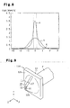
- Fig. 7 shows the intensity distribution of light along an imaginary lateral plane (along the X direction of Figs. 6(a) to 6(b)) containing the center ⁇ of each minute opening 25, 15, 35.
- Fig. 8 shows the intensity distribution of light along an imaginary vertical plane (along the Y direction of Figs. 6(a) to 6(b)) containing the center ⁇ of each minute opening 25, 15, 35.
- Figs. 7 shows the intensity distribution of light along an imaginary lateral plane (along the X direction of Figs. 6(a) to 6(b)) containing the center ⁇ of each minute opening 25, 15, 35.
- Fig. 8 shows the intensity distribution of light along an imaginary vertical plane (along the Y direction of Figs. 6(a) to 6(b)) containing the center ⁇ of each minute opening 25, 15, 35.
- curves a represent the intensity distribution of light that has passed through the minute opening 15 of this embodiment
- curves b represent the intensity distribution of light that has passed through the minute opening 25 of the comparison example 1
- curves c represent the intensity distribution of light that has passed through the minute opening 35 of the comparison example 2.
- the light intensity is significantly increased in the vicinity of the center ⁇ .
- surface plasmons are coupled to each other at the facing interfaces S in the narrow section 16 and enhances the electromagnetic intensity.
- Another reason is that the phase velocity of surface plasmons is decreased the surface of the narrow section 16, and light transmitted through the optical waveguide 13 converges to the narrow section 16.
- the case of the minute opening 25 of the comparison example 1 is examined. As shown by the curves b, the maximum value of the light intensity distribution is at the center O of the minute opening 25. One of the reasons for this is considered that surface plasmons at the facing interfaces are coupled to each other. Compared to the case of the minute opening 15 of this embodiment expressed by curves a, the electric field intensity is low in the comparison example 1. This is because the shape of the opening 25 is rectangular having the constant width along the longitudinal direction. In other words, the minute opening 25 does not have the narrow section 16 and the wide sections 17, which are continuously formed.
- the opening 25 of the comparison example 1 is less effective in decreasing the phase velocity of the surface plasmon to converge transmitted light.
- the minute opening 25 is as effective as the minute opening 15 in causing surface plasmons generated at the interfaces to be coupled to each other, thereby increasing the electric field intensity. Accordingly, the comparison example 1 has the same technical ideas as this embodiment and can be regarded as a modification of the embodiment.
- the light intensity is slightly increased as shown by the curves c at the left and right interfaces where surface plasmons are generated.
- the light intensity is scarcely increased at the center ⁇ of the minute opening 35. That is, in the case of minute opening 35 of the comparison example 2, the electric field intensity is not increased by coupling of surface plasmons generated at the interfaces. Therefore, the minute opening 35 does not decrease the phase velocity of surface plasmons to converge transmitted light, is therefore not suitable for practical use.
- the optical waveguide device has the following advantages.
- optical waveguide device 11C is an optical probe.
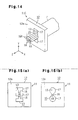
- the fourth embodiment is the same as the second embodiment except for the shape of a projection formed on the front portion 12a of the main body 12. Accordingly, differences from the first and second embodiments will mainly be discussed below, and like or the same reference numerals are given to those components that are like or the same as the corresponding components of the first and second embodiments.
- the optical waveguide device (optical probe) 11C of this embodiment includes a main body 12, which is a metal plate.
- the main body 12 is made of silver (Ag).
- an optical waveguide 13 is formed in the main body 12 along the thickness direction.
- Thin pillar shaped projections 12c are formed on the front portion 12a.
- the projections 12c are formed by further extending step portions defining the narrow section 16 along the direction in which transmitted light is emitted from the minute opening 15.
- the widths and lengths of the narrow section 16 and the wide sections 17 in the optical waveguide 13 (and in the minute opening 15) are the same as those in the optical waveguide device 11A according to the second embodiment.
- the height of the projections 12c is 202 nm, which is the same as the height of the projection 12b of the second embodiment.
- a predetermined light the wavelength of which is 488 nm is used.
- the predetermined light is a plane wave of linear polarization, and its polarization direction is the X direction as viewed in Fig. 14.
- the phenomenon described below takes place. That is, as in the previous embodiments, surface plasmons are generated on the inner surface of the optical waveguide 13. The electric fields of the surface plasmons are coupled to each other. As a result, the electric field intensity is increased. Therefore, due to the coupling of the electric fields, the intensity of light transmitted through the optical waveguide 13 is increased.
- the transmitted light with the increased intensity emerges out of the minute opening 15 (specifically, out of a region between the peaks of the projection 12c) as a spotlight (near-field light).
- the divergence of the spotlight (near-field light) emerging out of the minute opening 15 is further less than that of the first embodiment. That is, the bright zone of the spotlight with an increased intensity and the twilight zone about the bright zone are both small. This is favorable for increasing a resolution and a data recording density in optical processing. The bright zone and the twilight zone are minimized for the same reasons as the case of the optical waveguide device 11A of the second embodiment. That is, the minute opening 15 does not lie along a plane perpendicular to the direction along which light is transmitted through the optical waveguide 13, but lies along a projected plane that includes the distal ends of the thin pillar shaped projections 12c. Detailed description of the operation has been given in the second embodiment and is omitted in this embodiment.
- the optical waveguide device 11C according to the fourth embodiment has the same advantages as the advantages (1) to (5) of the optical waveguide device 11 according to the first embodiment, and the advantages (6) and (7) of the optical waveguide device 11A according to the second embodiment.
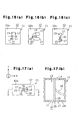
- Each of the above illustrated embodiment has only one narrow section 16. However, as shown in Fig. 15(a), two narrow sections 16 and three wide sections 17 may be formed alternately to form an opening. This structure generates two spotlights with an increased light intensity. In short, as long as at least one narrow section 16 is formed adjacent to wide sections 17 in the minute opening 15, the number of the narrow section 16 may be more than one.
- the minute opening 15 including the narrow section 16 and the wide sections 17 is formed with straight lines.
- the minute opening 15 may be formed with curved lines.
- the minute opening 15 may be shaped like a dumbbell as shown in Fig. 15(b).
- the minute opening 15 may be formed with a combination of straight lines and curved lines.
- the minute opening 15 is formed symmetrical.
- the shape of the opening 15 may be changed arbitrarily.
- the minute opening 15 may be asymmetrical.
- An excessively short length (represented by ay in Fig. 2) of the narrow section 16 not only mechanically weakens the minute opening 15, but also hinders surface plasmons from being generated on the parts 18 of the narrow section 16.
- any cross-section of the optical waveguide 13 perpendicular to the light transmission direction is the same as the shape of the minute opening 15.
- the cross-section of the optical waveguide 13 varies in the light transmission direction.
- a cross-section of the optical waveguide 13 may be larger in the main body 12 than the minute opening 15.
- the narrow section 16 and the wide sections 17 may be continuous along the X direction (lateral direction).
- the narrow section 16 is located at a center of the cross-section perpendicular to the light transmission direction of the optical waveguide 13.
- the narrow section 16 may be displaced from a center of the cross-section of the optical waveguide 13.
- the ratio of the width of the wide sections 17 to the width of the narrow section 16 may be considerably greater than those in the above illustrated embodiments. That is, as long as the width of the wide sections 17 is greater than the width of the narrow section 16, the width of the wide sections 17 may be infinite.
- the optical waveguide 13 extends through the main body 12. That is, the optical waveguide 13 is formed like a tunnel. However, as shown in Figs. 19(a) to 20(b), the optical waveguide 13 may be formed like a groove formed in the surface of the main body 12. In the modification shown in Figs. 19(a) and 19(b), a narrow section 16 is formed from the upper surface of the main body 12, and a wide section 17 is formed below and continuously to the narrow section 16. In the modification shown in Figs. 20(a) and 20(b), a rectangular groove having a narrow section 16 is formed from the upper surface of the main body 12. The operating principle of the modification shown in Figs.
- the distal opening of an optical waveguide according to the present invention includes not only the distal opening (the minute opening 15 shown in Fig. 1 and other drawings) of the optical waveguide 13 extending through the main body 12, but also the distal opening (the distal minute opening 15 shown in Figs. 19(a) and 20(a)) of the optical waveguide 20, which opening is formed as a groove on one side of the main body 12.
- a wide section 17, a narrow section 16, and a wide section 17 may be formed by machining from the surface of the main body 12 in this order.
- the narrow section 16 of the optical waveguide 13 is located close to the surface of the main body 12. In this case, the intensity of transmitted light is maximized at a part close to the surface of the main body 12.
- a number of optical waveguides need to be arranged with narrow spaces in between. If groove like optical waveguides are formed in such an optical integrated circuit, short circuits may be established due to light emerging from the waveguides to the surface of the main body.
- one of the wide sections 17 is exposed to the surface of the main body 12. Also, the narrow section 16, at which the light intensity is maximum, is away from the surface of main body 12. This structure is very advantages in preventing short circuits among the optical waveguides 13.
- openings are formed at both ends of the optical waveguide 13.
- the minute opening 15 may be formed in the optical waveguide 13. That is, in the modification of Figs. 17(a) and 17(b), the back opening 14 may be closed.
- light that enters the optical waveguide 13 through the minute opening 15 is reflected by the wall at the bottom and produces a standing wave. The light is then guided out of the minute opening 15.
- This structure is favorable for an illumination collection mode.
- the narrow section 16 (and the inner parts 18) is formed along a straight line in the optical waveguide 13.
- the narrow section 16 permits surface plasmons to couple to each other, thereby increasing the electrical field intensity.
- the narrow section 16 also decreases the phase velocity of surface plasmons, thereby converging transmitted light.
- the narrow section 16 (and the inner parts 18) may be branched in the optical waveguide 13. In this case, an additional distal opening like the minute opening 15 may be formed to correspond to the distal end of the branched narrow section 16.
- the narrow section 16 may be branched not only into two parts, but also into three parts. Alternatively, the narrow section 16 may be branched into a number of parts at a number of locations.
- optical waveguide 13 is used in an optical integrated circuit. That is, in an optical integrated circuit, optical waveguides must be routed (bent and branched) in a two-dimensional plane for forming a circuit with thin optical intensity distributions of nanometers.
- a circuit in which optical waveguides are routed in a two-dimensional plane parallel to an electric field is referred to as an E-plane circuit.
- a circuit in which optical waveguides are routed in a two-dimensional plane parallel to a magnetic field is referred to as an H-plane circuit.
- the narrow section 16 (and the inner parts 18) is branched.
- the electric field of the optical waveguide 13 chiefly lies along the Y direction, and the magnetic field chiefly lies along the X direction. Since the narrow section 16 is branched in a two-dimensional plane parallel to the magnetic field of the X direction, the optical waveguide 13 forms an H-plane circuit.
- the narrow section 16 (and the inner parts 18) is branched.
- the electric field of the optical waveguide 13 chiefly lies along the X direction, and the magnetic field chiefly lies along the Y direction. Since the narrow section 16 is branched in a two-dimensional plane parallel to the electric field of the X direction, the optical waveguide 13 forms an E-plane circuit.
- an H-plane circuit is formed, and the parts of the narrow section 16 face each other along the Y direction.
- a superfine optical circuit along the branched narrow section 16 is formed even if the width of each wide section 17 is infinite along the Y direction.
- an E-plane circuit is formed, and the parts of the narrow section 16 face each other along the X direction.
- a superfine optical circuit along the branched narrow section 16 is formed even if the width of each wide section 17 is infinite along the X direction.
- the embodiment shown in Figs. 19(a) and 19(b) may be modified as shown in Figs. 22 to 24.
- two narrow sections 16 are formed.
- the lower parts of the narrow sections 16 are connected to each other by a single wide section 17.
- the modification of Figs. 23 is the same as the modification of Fig. 22 except for that the optical waveguide 13 is filled with a dielectric medium other than the outside (air).
- the optical waveguide 13 is filled with glass.
- the cross-section of the optical waveguide 13 is formed with irregular curved lines.
- the optical waveguide 13 may be filled with a dielectric medium such as glass.
- silver (Ag) in which the real part of the relative complex permittivity is minus 7.38 is used as a plasmon activating medium.
- the real part of the relative complex permittivity is a minus value
- other types of silver (Ag) may be used.
- gold (Au) platinum, an alloy of gold and platinum, other metal materials, or semiconductor materials may be used.
- the entire main body 12 surrounding the optical waveguide 13 is made of a plasmon activating medium (silver Ag).
- a plasmon activating medium (silver Ag)
- other parts may be made of materials other than a plasmon activating medium.
- a plasmon activating medium (silver Ag) may be evaporated onto the inner surface of the optical waveguide 13 including the parts 18 of the narrow section 16.
- the width aX of the narrow section 16 of the minute opening 15 is set to a predetermined value (for example, 31 nm). As long as the width aX is less than the half of the wavelength of transmitted light, the width aX may be changed. Also, the measurement L along the Y direction, which intersects the width direction (X direction) of the minute opening 15 may be changed from the ones presented above. That is, as long as the measurement L is greater than the measurement calculation value, the measurement L may be greater than the half of the wavelength of transmitted light.
- the cross-section of the optical waveguide 13 perpendicular to the light transmission direction is the same as the minute opening 15 and is constant towards the back opening 14.
- the shape of the optical waveguide 13 may be changed.
- the optical waveguide 13 may be tapered such that the area of the cross-section decreases from the back opening 14 to the distal minute opening 15.
- a medium that forms the interfaces S with the inner surface of the optical waveguide 13 is air.
- the optical waveguide 13 may be filled with a dielectric medium such as glass.
- the narrow section 16 is formed along the entire inner surface of the optical waveguide 13.
- the narrow section 16 may be formed only at the minute opening 15, which is the distal opening of the optical waveguide 13.
- a part similar to the minute opening 15 having the narrow section 16 and the wide sections 17, which are formed continuously, may be provided midway in the light transmission direction of the optical waveguide 13. In this case, the distal opening and the back opening (back side) are wider than the wavelength of transmitted light.
- the projection 12b is conical. However, as long as the projection 12b is shaped like a pyramid.
- each projection 12c is shaped like a thin pillar of a rectangular cross-section. However, as long as a narrow section is defined between the pillars, the each projection 12c may have a semicircular cross-section or a thin extended rectangular cross-section.
- the optical waveguide device 41 is an exposure mask (including a reticle).
- An exposure mask is used in a projection exposure system, which is referred to as stepper. Specifically, an exposure mask is used when a circuit pattern is formed on a semiconductor substrate, on which sensitive material is applied, through lithography, or through projection and exposure.
- the optical waveguide device (exposure mask) 41 of this embodiment includes a main body 42, which is a rectangular metal plate.
- the main body 12 is made of silver (Ag).
- An optical waveguide 13 is formed in the main body 42 along the thickness direction.
- a minute opening 15 is formed on a front portion 42a and a back portion (not shown) of the main body 42.
- the minute opening 15 functions as end openings (a distal opening and a proximal opening).
- the width of the minute opening 15 is less than the wavelength of light.
- the minute opening 15 has a narrow section 16 and a pair of wide sections 17, which are arranged alternately .
- the narrow section 16 is substantially located in a center of the front portion 42a.
- the width of each of the narrow section 16 and the wide sections 17 is defined as the measurement along the polarization direction of light transmitted through the optical waveguide 13, or the measurement along the lateral direction as viewed in Fig. 25.
- the narrow section 16 and the wide sections 17 are continuously formed along a direction perpendicular to the width direction.
- the width of the narrow section 16 is 16 nm, and the width of each wide section 17 is 47 nm.
- the length of the narrow section 16 is 280 nm, and the length of each wide section 17 is 93 nm.
- the thickness of the main body 42 is 78 nm. Therefore, the length of the minute opening 15 is 466 nm.
- the main body 42 of the device 41 is placed on a semiconductor substrate 43 as shown in Fig. 26.
- a sensitive material such as novolac resin is applied to the surface of the semiconductor substrate 43 in advance to form a sensitive material layer 44.
- the main body 42 closely contacts the sensitive material layer 44.
- a transparent glass plate 45 is placed on the main body 42, and projection light is irradiated from above. That is, as in the above illustrated embodiments, light the wavelength of which is 488 nm is used.
- the light is a plane wave of linear polarization, and its polarization direction is the lateral direction as viewed in Fig. 26.
- the light enters the optical waveguide 13 of the main body 42 as a projection light. At this time, the following phenomenon takes place in the optical waveguide 13 of the optical waveguide device 41.
- the intensity of light transmitted through the optical waveguide 13 is increased.
- the transmitted light with the increased intensity emerges out of the narrow section 16 of the minute opening 15 as a thin line spotlight (near-field light) along the longitudinal narrow section 16.
- the sensitive material layer 44 on the semiconductor substrate 43 is exposed to the thin line spotlight. Thereafter, unnecessary part of the sensitive material layer 44 is removed through a conventional etching. Accordingly, a circuit pattern is formed on the semiconductor substrate 43. A linear part of a wiring pattern of the circuit pattern corresponds to the thin line spot light.
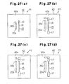
- Fig. 27(a) is a front view of an optical waveguide device 41 having an optical waveguide 13 (and a minute opening 15) the cross-section of which perpendicular to a light transmission direction of a main body 42 consists only of a narrow section 16 and is an extended rectangle. Figs.
- FIG. 27(b) and 27(d) are front views of optical waveguide devices 41 each having an optical waveguide 13, in which a narrow section 16 and wide sections 17 are continuously formed.
- Fig. 27(c) is front view of an optical waveguide device 41 according to this embodiment, which has the optical waveguide 13 and the minute opening 15 of the above described measurements.
- the width of the minute opening 15, or the width of the optical waveguide 13 of the of the optical waveguide device 41 shown in Fig. 27(a), is 16 nm, which is the same as the width of the narrow section 16 of the minute opening 15 according to the fifth embodiment.
- the length of the minute opening 15 (and the narrow section 16), or the longitudinal measurement of the minute opening 15, is 280 nm, which is the same as the measurement of the narrow section 16 of this embodiment.
- the minute opening 15 of the optical waveguide 13 in the optical waveguide device 41 shown in Fig. 27(b) is the same as that of this embodiment except for that the length of each wide section is less than that of this embodiment (93 nm), for example, 62 nm.
- the minute opening 15 of the optical waveguide 13 in the optical waveguide device 41 shown in Fig. 27(d) is the same as that of this embodiment except for that the length of each wide section is more than that of this embodiment (93 nm), for example, 109 nm.
- a bright zone 20a of each spotlight and a twilight zone 20b of the peripheral light are is shown by broken lines and two-dot chain lines to the left of each minute opening 15 in Figs. 27(a) through 27(d).
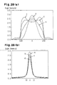
- Fig. 28(a) shows the intensity distribution of light along a vertical imaginary plane containing the center of the minute opening 15 in each of Figs. 27(a) to 27(d), when a light passes through the optical waveguide 13 of the optical waveguide device 41 shown in each of Figs. 27(a) to 27(d) under the same conditions.
- Fig. 28(b) shows the intensity distribution of light along a lateral imaginary plane containing the center of the minute opening 15 in each of Figs. 27(a) to 27(d).
- curves a represent light intensity distributions of the light that has passed through the minute opening 15 shown in Fig.
- curves b represent light intensity distributions of the light that has passed through the minute opening 15 shown in Fig. 27(b).
- curves c represent light intensity distributions of the light that has passed through the minute opening 15 shown in Fig. 27(c)
- curves d represent light intensity distributions of the light that has passed through the minute opening 15 shown in Fig. 27(d).
- the light intensity is high at in a range including the center of the minute opening 15.
- the bright zone 20a is not expanded to the longitudinal ends of the minute opening 15.
- the ends are in twilight zones 20b and light intensity is low.
- the bright zone 20a expands to the longitudinal ends of the minute opening 15.
- the light intensity varies significantly along the entire length of the minute opening 15.
- the light intensity is maximum at the longitudinal ends of the minute opening 15, and is less at the center.
- the light intensity of the optical waveguide device 41 shown in Fig. 27(c) is relatively high and scarcely varies along the entire length of the narrow section of the narrow section 16 of the minute opening 15. That is, in accordance with the measurements of the narrow section 16, a spotlight with an even light intensity is obtained.
- the width and the length of the spotlight is 16 nm and 280 nm, respectively.
- Figs. 28(a) and 28(b) show cases where the light intensity of the incident light is represented by 1.0. As shown in Figs. 28(a) and 28(b), the intensity of the emitted light is 2.3 times the intensity of incident light.
- the optical waveguide device 41 of this embodiment has the following advantages.
- optical waveguide device 41 according to the fifth embodiment may be modified as follows.
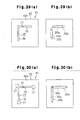
- the cross-section of the optical waveguide 13 perpendicular to the light transmission direction and the minute opening 15 may be shaped like a letter L when viewed from front. That is, the optical waveguide 13 and the minute opening 15 may have two narrow sections 16 that are connected to each other at the ends and form a right angle. This permits a perpendicular part of a circuit pattern to be easily formed. In this case, wide sections are preferably formed in the vicinity of the perpendicular joint between the narrow sections 16. This point will be discussed below.
- the minute opening 15 of the optical waveguide 13 is L-shaped. Narrow sections 16 are connected to each other to form a right angle. No wide section 17 is formed in the minute opening 15.
- Fig. 29(b) shows the distribution of spotlight emerging out of the minute opening of Fig. 29(a).
- bright zones 20a, as well as twilight zones 20b are not connected to each other. Therefore, the optical waveguide device 41 of Fig. 29(a) cannot be used for forming perpendicular parts in a circuit pattern.
- the minute opening 15 of the optical waveguide 13 is L-shaped. Narrow sections 16 are connected to each other to form a right angle. Also, a wide section 17 is formed at the end of each narrow section 16. Also, a wide section 17 is formed at the joint of the narrow sections 16, where the narrow sections 16 intersect perpendicularly. Therefore, when a horizontally polarized wave the polarization direction of which is the lateral direction in Fig. 30(a) and a vertically polarized wave the polarization direction of which is the vertical direction in Fig. 30(a) enter the optical waveguide 13 of the optical waveguide device 41, bright zones 20a and twilight zones 20b shown in Fig. 30(b) are produced. That is, in accordance with the widths and the lengths of the narrow sections 16, linear spotlights with an even light intensity are obtained. The spotlights form a letter L.
- the optical waveguide device 51 is a polarizer.
- a polarizer is a device for obtaining a polarized light in a predetermined direction from a light containing polarized lights in all directions, such as natural light.
- a polarizer is also used for checking if there is any polarized light.
- a polarizer is used as a spectroscope for disintegrating into spectrums.
- the optical waveguide device (polarizer) 51 of this embodiment includes a main body 52, which is a rectangular metal plate.
- the main body 12 is made of silver (Ag).
- Optical waveguides 13 are formed in the main body 52 along the thickness direction. In this embodiment, the number of the optical waveguide 13 is three.
- Minute openings 15 are formed on a front portion 42a and a back portion (not shown) of the main body 52. The minute openings 15 function as end openings (distal openings and proximal openings). The width of each minute opening 15 is less than the wavelength of light.
- each minute opening 15 according to the sixth embodiment is formed like an extended rectangle. That is, each minute opening 15 has no wide sections, and its width is constant long the entire length. In other words, the minute opening 15 is a linear slit.
- the minute openings 15 each forming a narrow section 16 are arranged parallel to each other.
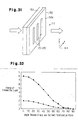
- the width of each minute opening 15 is defined as the measurement along the polarization direction of light transmitted through the corresponding optical waveguide 13, or the measurement along an X direction as viewed in Fig. 31.
- Each minute opening 15 is formed as a rectangle extended along a direction perpendicular to the width direction, or along the Y direction as viewed in Fig. 31.
- the actual size of each minute opening 15 is significantly small compared to the size of the main body 52 (and the front portion 52a), the size of the minute opening 15 is exaggerated in Fig. 31.
- each minute opening 15 which is also the narrow section 16, is 16 nm.
- the length of each minute opening 15 (and each narrow section 16), which is also the measurement of the minute opening 15, is, for example, 559 nm.
- the thickness of the main body 52 is, for example, 78 nm.
- the interval between each adjacent pair of the minute openings 15 is 62 nm.
- a glass substrate 53 is fixed to a back of the main body 52, or to a side opposite from the front portion 52a.
- light represented by arrows in Fig. 31 enters the optical waveguides 13 from the back (the glass substrate 53) of the optical waveguide device 51, and the wavelength of the light is 488 nm.
- a light component in the incident light that is polarized in the X direction passes through the optical waveguides 13 and is emitted from the minute openings 15 in the Z direction as a transmitted light.
- a light component that is polarized in the Y direction in Fig. 31 is not transmitted and emitted. Therefore, light the polarization direction is perpendicular to the longitudinal direction of the minute openings 15 (the Y direction in Fig. 31) passes through and is emitted from the device 51.
- the area of the optical waveguides 13 (and the minute openings 15) of the optical waveguide device (polarizer) 51 is extremely small compared to the entire area of the front portion 52a of the main body 52.
- the main body 52 is made of a dielectric medium (plasmon activating medium) whose real part of the relative complex permittivity is negative, or silver (Ag), in which the real part of the relative complex permittivity is minus 7.38 when the wavelength of transmitted light is 488 nm in this embodiment.
- the electric field intensity of a light component polarized in the X direction in the light entering the optical waveguide 13 is increased.
- the light component with the increased intensity is emitted as transmitted light.
- the reason for this is that, as in the above illustrated embodiments, the electric fields of surface plasmons produced at the inner surfaces of each optical waveguide 13 are coupled to each other at the interfaces in the width direction.
- the light that enters each optical waveguide 13 includes light components.
- the angle defined by the incident polarization plane and the X axis is not zero degrees for some of the light components. Among the light components with angles other than zero degrees, light components with a small angle is slightly emitted from the minute opening 15 of the optical waveguide 13. This phenomenon will now be described with reference to Fig. 32.
- the horizontal axis represents the angle defined by the X axis of Fig. 31 and the incident polarization plane of light (polarized light) that enters each optical waveguide 13. If the angle of a light is ninety degrees, the polarization direction of the light is the Y direction in Fig. 31. If the angle of a light is zero degrees, the polarization direction of the light is the X direction in Fig. 31.
- the vertical axis represents the energy of transmitted light through each optical waveguide 13 (and the minute opening 15). Specifically, the energy of incident light in a unit area of each optical waveguide 13 is defined as one, and the energy of the transmitted light is measured based on this value. In Fig.
- black circular spots represent the results of a simulation performed on the assumption that there is only one optical waveguide 13, and the width and the length of the waveguide 13 is 16 nm and 559 nm, respectively.
- Black square spots represents the results of a simulation performed on the assumption that there are two parallel optical waveguides 13 of the same measurements as the first simulation.
- the energy of transmitted light is greater when the angle defined by the incident polarization plane and the X axis is closer to zero degrees. This tendency is stronger in the case of the black square spots, where the two parallel optical waveguides 13 are provided, compared to the case of the black circular spots, where only one optical waveguide 13 is provided.
- energy is measured with a unit area that is defined according to the wave number (2 ⁇ /wavelength). Specifically, the energy in a unit area of a square each side of which is 78 nm (78 nm ⁇ 78 nm square) is defined as one.
- P1 represents the energy of a transmitted light when the angle defined by the incident polarization plane and the X axis is zero degrees.
- P2 represents the energy of a transmitted light when the angle defined by the incident polarization plane and the X axis is ninety degrees.
- the incident energy was 2.88, and the energy of the transmitted energy was 8.00.
- the optical waveguide device 51 (the polarizer) of this embodiment has the following advantages.
- the sixth embodiment simplifies the structure of the polarizer (polarizing plates) used in a spectroscope and thus reduces the cost. Also, the sixth embodiment permits the intensity of a polarized light component to be increased so that light with an increased intensity is emitted.
- optical waveguide device 51 according to the sixth embodiment may be modified as follows.
- the number of the optical waveguides 13 is arbitrarily changed as long as there are one or more waveguides 13. As long as the minute openings 15 (narrow sections 16) of the optical waveguides 13 are parallel, the minute openings 15 need not extend along the X direction in Fig. 31. That is, referring to Fig. 32, as long as a desired amount of energy of transmitted light is obtained, each minute opening 15 may extend in a direction that intersects the X direction at a predetermined angle.
Landscapes
- Physics & Mathematics (AREA)
- General Physics & Mathematics (AREA)
- Optics & Photonics (AREA)
- Engineering & Computer Science (AREA)
- Chemical & Material Sciences (AREA)
- Nanotechnology (AREA)
- Microelectronics & Electronic Packaging (AREA)
- Health & Medical Sciences (AREA)
- General Health & Medical Sciences (AREA)
- Nuclear Medicine, Radiotherapy & Molecular Imaging (AREA)
- Radiology & Medical Imaging (AREA)
- Crystallography & Structural Chemistry (AREA)
- Analytical Chemistry (AREA)
- Life Sciences & Earth Sciences (AREA)
- Biophysics (AREA)
- Optical Head (AREA)
- Optical Integrated Circuits (AREA)
- Investigating Or Analysing Materials By Optical Means (AREA)
- Exposure And Positioning Against Photoresist Photosensitive Materials (AREA)
- Exposure Of Semiconductors, Excluding Electron Or Ion Beam Exposure (AREA)
- Light Guides In General And Applications Therefor (AREA)
Applications Claiming Priority (4)
| Application Number | Priority Date | Filing Date | Title |
|---|---|---|---|
| JP2002217084 | 2002-07-25 | ||
| JP2002217084 | 2002-07-25 | ||
| JP2003018997A JP3668779B2 (ja) | 2002-07-25 | 2003-01-28 | 光導波装置 |
| JP2003018997 | 2003-01-28 |
Publications (2)
| Publication Number | Publication Date |
|---|---|
| EP1385175A1 true EP1385175A1 (fr) | 2004-01-28 |
| EP1385175B1 EP1385175B1 (fr) | 2007-04-25 |
Family
ID=30002395
Family Applications (1)
| Application Number | Title | Priority Date | Filing Date |
|---|---|---|---|
| EP03254624A Expired - Lifetime EP1385175B1 (fr) | 2002-07-25 | 2003-07-24 | Design d'un embout de sonde pour un microscope à champs proche |
Country Status (6)
| Country | Link |
|---|---|
| US (1) | US6947634B2 (fr) |
| EP (1) | EP1385175B1 (fr) |
| JP (1) | JP3668779B2 (fr) |
| CN (1) | CN1284986C (fr) |
| DE (1) | DE60313403T2 (fr) |
| SG (1) | SG105581A1 (fr) |
Cited By (1)
| Publication number | Priority date | Publication date | Assignee | Title |
|---|---|---|---|---|
| GB2528576A (en) * | 2014-07-23 | 2016-01-27 | HGST Netherlands BV | A split-ring resonator (SRR) NFT design for use in HAMR |
Families Citing this family (27)
| Publication number | Priority date | Publication date | Assignee | Title |
|---|---|---|---|---|
| JP4289918B2 (ja) * | 2003-05-01 | 2009-07-01 | キヤノン株式会社 | 位置検出装置、及び該位置検出装置を有するアライメント装置 |
| KR100868246B1 (ko) * | 2004-06-11 | 2008-11-11 | 기후고꾸리츠 다이가꾸호오징 기후다이가꾸 | 광도파 장치 |
| TW200540477A (en) * | 2004-06-11 | 2005-12-16 | Univ Gifu | Optical waveguide device |
| JP4574250B2 (ja) * | 2004-06-30 | 2010-11-04 | キヤノン株式会社 | フォトマスク |
| WO2007018230A1 (fr) * | 2005-08-10 | 2007-02-15 | Osaka University | Sonde optique |
| US8675199B2 (en) | 2006-03-10 | 2014-03-18 | Plc Diagnostics, Inc. | Waveguide-based detection system with scanning light source |
| US9528939B2 (en) | 2006-03-10 | 2016-12-27 | Indx Lifecare, Inc. | Waveguide-based optical scanning systems |
| US9976192B2 (en) | 2006-03-10 | 2018-05-22 | Ldip, Llc | Waveguide-based detection system with scanning light source |
| US7951583B2 (en) | 2006-03-10 | 2011-05-31 | Plc Diagnostics, Inc. | Optical scanning system |
| US9423397B2 (en) | 2006-03-10 | 2016-08-23 | Indx Lifecare, Inc. | Waveguide-based detection system with scanning light source |
| US8288157B2 (en) | 2007-09-12 | 2012-10-16 | Plc Diagnostics, Inc. | Waveguide-based optical scanning systems |
| US7800193B2 (en) | 2006-03-13 | 2010-09-21 | Nec Corporation | Photodiode, method for manufacturing such photodiode, optical communication device and optical interconnection module |
| US9046649B2 (en) | 2006-08-31 | 2015-06-02 | Micron Technology, Inc. | Communication methods, methods of forming an interconnect, signal interconnects, integrated circuit structures, circuits, and data apparatuses |
| US7844142B2 (en) * | 2006-08-31 | 2010-11-30 | Micron Technology, Inc. | Communication methods, methods of forming an interconnect, signal interconnects, integrated circuit structures, circuits, and data apparatuses |
| KR100783365B1 (ko) | 2006-09-29 | 2007-12-07 | 한국전자통신연구원 | 광도파로 소자 |
| KR100846515B1 (ko) * | 2007-03-19 | 2008-07-17 | 삼성전자주식회사 | 테이퍼진 c-형 개구를 갖는 90도 굽어진 금속 도파로,상기 도파로의 제조 방법, 상기 도파로를 이용한 광전송모듈 및 상기 도파로를 채용한 열보조 자기기록 헤드 |
| US8467637B2 (en) | 2007-05-01 | 2013-06-18 | Nec Corporation | Waveguide path coupling-type photodiode |
| GB2461026B (en) | 2008-06-16 | 2011-03-09 | Plc Diagnostics Inc | System and method for nucleic acids sequencing by phased synthesis |
| JP4520524B2 (ja) * | 2008-11-04 | 2010-08-04 | 株式会社日立製作所 | 熱アシスト記録用磁気ヘッドスライダ及びそれを用いた熱アシスト記録装置 |
| US8092704B2 (en) | 2008-12-30 | 2012-01-10 | Hitachi Global Storage Technologies Netherlands B.V. | System, method and apparatus for fabricating a c-aperture or E-antenna plasmonic near field source for thermal assisted recording applications |
| US7880996B2 (en) * | 2008-12-31 | 2011-02-01 | Hitachi Global Storage Technologies Netherlands B.V. | Ridge wave-guide for thermal assisted magnetic recording |
| US20110292774A1 (en) * | 2009-02-17 | 2011-12-01 | Kou Osawa | Near-field light emitting device, optical recording head and optical recorder |
| US10018566B2 (en) | 2014-02-28 | 2018-07-10 | Ldip, Llc | Partially encapsulated waveguide based sensing chips, systems and methods of use |
| WO2016138427A1 (fr) | 2015-02-27 | 2016-09-01 | Indx Lifecare, Inc. | Système de détection à guide d'ondes à source de lumière à balayage |
| US9472230B1 (en) * | 2015-04-20 | 2016-10-18 | Headway Technologies, Inc. | Plasmon generator including a main body and a front protrusion |
| CN107271470B (zh) * | 2017-04-19 | 2019-03-29 | 电子科技大学 | 一种太赫兹波传输聚束系统 |
| JP7031856B2 (ja) * | 2018-02-14 | 2022-03-08 | 国立大学法人東京工業大学 | ビーム偏向デバイス |
Citations (2)
| Publication number | Priority date | Publication date | Assignee | Title |
|---|---|---|---|---|
| EP0185782A1 (fr) * | 1984-12-28 | 1986-07-02 | International Business Machines Corporation | Guide d'ondes pour un microscope optique de champ proche |
| WO2002010830A2 (fr) * | 2000-07-27 | 2002-02-07 | Zetetic Institute | Reseaux a sources multiples pour microscopie a champ proche |
Family Cites Families (8)
| Publication number | Priority date | Publication date | Assignee | Title |
|---|---|---|---|---|
| US5789742A (en) * | 1996-10-28 | 1998-08-04 | Nec Research Institute, Inc. | Near-field scanning optical microscope probe exhibiting resonant plasmon excitation |
| JP3513448B2 (ja) * | 1999-11-11 | 2004-03-31 | キヤノン株式会社 | 光プローブ |
| EP1247122A1 (fr) | 1999-12-23 | 2002-10-09 | Spectalis Corporation | Structures de guide d'ondes optique |
| JP3574794B2 (ja) | 2001-06-05 | 2004-10-06 | 独立行政法人 科学技術振興機構 | プローブ及びその製造方法 |
| EP1402293A1 (fr) | 2001-06-22 | 2004-03-31 | Spectalis Corporation | Structures de guide d'ondes optiques |
| JP4245117B2 (ja) | 2001-06-22 | 2009-03-25 | セイコーインスツル株式会社 | 光情報記録再生装置 |
| US6549687B1 (en) * | 2001-10-26 | 2003-04-15 | Lake Shore Cryotronics, Inc. | System and method for measuring physical, chemical and biological stimuli using vertical cavity surface emitting lasers with integrated tuner |
| WO2004080430A2 (fr) * | 2003-03-13 | 2004-09-23 | 3M Innovative Properties Company | Procedes pour ameliorer la qualite de la peau |
-
2003
- 2003-01-28 JP JP2003018997A patent/JP3668779B2/ja not_active Expired - Lifetime
- 2003-07-24 EP EP03254624A patent/EP1385175B1/fr not_active Expired - Lifetime
- 2003-07-24 DE DE60313403T patent/DE60313403T2/de not_active Expired - Fee Related
- 2003-07-25 SG SG200303886A patent/SG105581A1/en unknown
- 2003-07-25 US US10/627,944 patent/US6947634B2/en not_active Expired - Fee Related
- 2003-07-25 CN CNB031438164A patent/CN1284986C/zh not_active Expired - Fee Related
Patent Citations (2)
| Publication number | Priority date | Publication date | Assignee | Title |
|---|---|---|---|---|
| EP0185782A1 (fr) * | 1984-12-28 | 1986-07-02 | International Business Machines Corporation | Guide d'ondes pour un microscope optique de champ proche |
| WO2002010830A2 (fr) * | 2000-07-27 | 2002-02-07 | Zetetic Institute | Reseaux a sources multiples pour microscopie a champ proche |
Non-Patent Citations (2)
| Title |
|---|
| JOHNSON P B ET AL: "OPTICAL CONSTANTS OF THE NOBLE METALS", PHYSICAL REVIEW, B. SOLID STATE, AMERICAN INSTITUTE OF PHYSICS. NEW YORK, US, vol. 6, no. 12, 15 December 1972 (1972-12-15), pages 4370 - 4379, XP001031007 * |
| U. SCHRÖTER, A. DEREUX: "Surface plasmon polaritons on metal cylinders with dielectric core", PHYSICAL REVIEW B, vol. 64, 11 September 2001 (2001-09-11), pages 125420-1 - 125420-10, XP002259671 * |
Cited By (1)
| Publication number | Priority date | Publication date | Assignee | Title |
|---|---|---|---|---|
| GB2528576A (en) * | 2014-07-23 | 2016-01-27 | HGST Netherlands BV | A split-ring resonator (SRR) NFT design for use in HAMR |
Also Published As
| Publication number | Publication date |
|---|---|
| CN1482473A (zh) | 2004-03-17 |
| SG105581A1 (en) | 2004-08-27 |
| JP3668779B2 (ja) | 2005-07-06 |
| EP1385175B1 (fr) | 2007-04-25 |
| US6947634B2 (en) | 2005-09-20 |
| DE60313403T2 (de) | 2007-09-06 |
| CN1284986C (zh) | 2006-11-15 |
| US20040062477A1 (en) | 2004-04-01 |
| DE60313403D1 (de) | 2007-06-06 |
| JP2004109965A (ja) | 2004-04-08 |
Similar Documents
| Publication | Publication Date | Title |
|---|---|---|
| EP1385175B1 (fr) | Design d'un embout de sonde pour un microscope à champs proche | |
| US7057151B2 (en) | Optical transmission apparatus with directionality and divergence control | |
| Fu et al. | Plasmonic lenses: a review | |
| US7068911B2 (en) | Optical probe and optical pick-up apparatus | |
| US8353061B2 (en) | Near-field scanning optical microscopy with nanoscale resolution from microscale probes | |
| US7359598B2 (en) | Surface plasmon optic devices and radiating surface plasmon sources for photolithography | |
| US7759630B2 (en) | Method and apparatus for the generation and control of multiple near-field light sources at subwavelength resolution | |
| US6970307B2 (en) | Optical near-field generating element and optical apparatus including the same | |
| JP4289918B2 (ja) | 位置検出装置、及び該位置検出装置を有するアライメント装置 | |
| CN1965226B (zh) | 光波导装置 | |
| JP4427343B2 (ja) | 近接場光学顕微鏡 | |
| JP3053380B2 (ja) | 光ファイバプローブ | |
| KR100868246B1 (ko) | 광도파 장치 | |
| KR20040036901A (ko) | 광중합에 의해 렌즈가 제공된 개선된 광섬유 및 그와연관된 새로운 광학 소자들 | |
| JP3268201B2 (ja) | 光ファイバプローブ | |
| JP2021179310A (ja) | 光検出装置、および光検出システム | |
| JP6101790B2 (ja) | 光結合装置および当該装置の製造方法 | |
| Mariani et al. | Scattering and absorption in 2D optics | |
| Hung | Studies of the optical properties of plasmonic nanostructures | |
| Ruiz | Probing ultra-subwavelength inhomogeneities embedded within dielectric targets using photonic nanojets |
Legal Events
| Date | Code | Title | Description |
|---|---|---|---|
| PUAI | Public reference made under article 153(3) epc to a published international application that has entered the european phase |
Free format text: ORIGINAL CODE: 0009012 |
|
| 17P | Request for examination filed |
Effective date: 20030724 |
|
| AK | Designated contracting states |
Kind code of ref document: A1 Designated state(s): AT BE BG CH CY CZ DE DK EE ES FI FR GB GR HU IE IT LI LU MC NL PT RO SE SI SK TR |
|
| AX | Request for extension of the european patent |
Extension state: AL LT LV MK |
|
| AKX | Designation fees paid |
Designated state(s): FR GB IT |
|
| 17Q | First examination report despatched |
Effective date: 20041011 |
|
| REG | Reference to a national code |
Ref country code: DE Ref legal event code: 8566 |
|
| GRAP | Despatch of communication of intention to grant a patent |
Free format text: ORIGINAL CODE: EPIDOSNIGR1 |
|
| RBV | Designated contracting states (corrected) |
Designated state(s): DE FR GB |
|
| GRAS | Grant fee paid |
Free format text: ORIGINAL CODE: EPIDOSNIGR3 |
|
| GRAA | (expected) grant |
Free format text: ORIGINAL CODE: 0009210 |
|
| AK | Designated contracting states |
Kind code of ref document: B1 Designated state(s): DE FR GB |
|
| RAP1 | Party data changed (applicant data changed or rights of an application transferred) |
Owner name: PRESIDENT OF GIFU UNIVERSITY |
|
| REG | Reference to a national code |
Ref country code: GB Ref legal event code: FG4D |
|
| REF | Corresponds to: |
Ref document number: 60313403 Country of ref document: DE Date of ref document: 20070606 Kind code of ref document: P |
|
| ET | Fr: translation filed | ||
| PGFP | Annual fee paid to national office [announced via postgrant information from national office to epo] |
Ref country code: GB Payment date: 20070516 Year of fee payment: 5 |
|
| PLBE | No opposition filed within time limit |
Free format text: ORIGINAL CODE: 0009261 |
|
| STAA | Information on the status of an ep patent application or granted ep patent |
Free format text: STATUS: NO OPPOSITION FILED WITHIN TIME LIMIT |
|
| 26N | No opposition filed |
Effective date: 20080128 |
|
| GBPC | Gb: european patent ceased through non-payment of renewal fee |
Effective date: 20080724 |
|
| PG25 | Lapsed in a contracting state [announced via postgrant information from national office to epo] |
Ref country code: GB Free format text: LAPSE BECAUSE OF NON-PAYMENT OF DUE FEES Effective date: 20080724 |
|
| PGFP | Annual fee paid to national office [announced via postgrant information from national office to epo] |
Ref country code: FR Payment date: 20090716 Year of fee payment: 7 |
|
| PGFP | Annual fee paid to national office [announced via postgrant information from national office to epo] |
Ref country code: DE Payment date: 20090722 Year of fee payment: 7 |
|
| REG | Reference to a national code |
Ref country code: FR Ref legal event code: ST Effective date: 20110331 |
|
| PG25 | Lapsed in a contracting state [announced via postgrant information from national office to epo] |
Ref country code: DE Free format text: LAPSE BECAUSE OF NON-PAYMENT OF DUE FEES Effective date: 20110201 |
|
| REG | Reference to a national code |
Ref country code: DE Ref legal event code: R119 Ref document number: 60313403 Country of ref document: DE Effective date: 20110201 |
|
| PG25 | Lapsed in a contracting state [announced via postgrant information from national office to epo] |
Ref country code: FR Free format text: LAPSE BECAUSE OF NON-PAYMENT OF DUE FEES Effective date: 20100802 |