EP1387220A2 - Justiermethode und -apparat eines optischen Systems, sowie Belichtungsapparat - Google Patents
Justiermethode und -apparat eines optischen Systems, sowie Belichtungsapparat Download PDFInfo
- Publication number
- EP1387220A2 EP1387220A2 EP03254724A EP03254724A EP1387220A2 EP 1387220 A2 EP1387220 A2 EP 1387220A2 EP 03254724 A EP03254724 A EP 03254724A EP 03254724 A EP03254724 A EP 03254724A EP 1387220 A2 EP1387220 A2 EP 1387220A2
- Authority
- EP
- European Patent Office
- Prior art keywords
- optical system
- light
- wave front
- front aberration
- multilayer
- Prior art date
- Legal status (The legal status is an assumption and is not a legal conclusion. Google has not performed a legal analysis and makes no representation as to the accuracy of the status listed.)
- Withdrawn
Links
Images


Classifications
-
- G—PHYSICS
- G02—OPTICS
- G02B—OPTICAL ELEMENTS, SYSTEMS OR APPARATUS
- G02B17/00—Systems with reflecting surfaces, with or without refracting elements
- G02B17/02—Catoptric systems, e.g. image erecting and reversing system
- G02B17/06—Catoptric systems, e.g. image erecting and reversing system using mirrors only, i.e. having only one curved mirror
- G02B17/0647—Catoptric systems, e.g. image erecting and reversing system using mirrors only, i.e. having only one curved mirror using more than three curved mirrors
- G02B17/0663—Catoptric systems, e.g. image erecting and reversing system using mirrors only, i.e. having only one curved mirror using more than three curved mirrors off-axis or unobscured systems in which not all of the mirrors share a common axis of rotational symmetry, e.g. at least one of the mirrors is warped, tilted or decentered with respect to the other elements
-
- H—ELECTRICITY
- H10—SEMICONDUCTOR DEVICES; ELECTRIC SOLID-STATE DEVICES NOT OTHERWISE PROVIDED FOR
- H10P—GENERIC PROCESSES OR APPARATUS FOR THE MANUFACTURE OR TREATMENT OF DEVICES COVERED BY CLASS H10
- H10P76/00—Manufacture or treatment of masks on semiconductor bodies, e.g. by lithography or photolithography
-
- B—PERFORMING OPERATIONS; TRANSPORTING
- B82—NANOTECHNOLOGY
- B82Y—SPECIFIC USES OR APPLICATIONS OF NANOSTRUCTURES; MEASUREMENT OR ANALYSIS OF NANOSTRUCTURES; MANUFACTURE OR TREATMENT OF NANOSTRUCTURES
- B82Y10/00—Nanotechnology for information processing, storage or transmission, e.g. quantum computing or single electron logic
-
- G—PHYSICS
- G02—OPTICS
- G02B—OPTICAL ELEMENTS, SYSTEMS OR APPARATUS
- G02B5/00—Optical elements other than lenses
- G02B5/08—Mirrors
- G02B5/0891—Ultraviolet [UV] mirrors
-
- G—PHYSICS
- G03—PHOTOGRAPHY; CINEMATOGRAPHY; ANALOGOUS TECHNIQUES USING WAVES OTHER THAN OPTICAL WAVES; ELECTROGRAPHY; HOLOGRAPHY
- G03F—PHOTOMECHANICAL PRODUCTION OF TEXTURED OR PATTERNED SURFACES, e.g. FOR PRINTING, FOR PROCESSING OF SEMICONDUCTOR DEVICES; MATERIALS THEREFOR; ORIGINALS THEREFOR; APPARATUS SPECIALLY ADAPTED THEREFOR
- G03F7/00—Photomechanical, e.g. photolithographic, production of textured or patterned surfaces, e.g. printing surfaces; Materials therefor, e.g. comprising photoresists; Apparatus specially adapted therefor
- G03F7/70—Microphotolithographic exposure; Apparatus therefor
- G03F7/70216—Mask projection systems
- G03F7/70258—Projection system adjustments, e.g. adjustments during exposure or alignment during assembly of projection system
-
- G—PHYSICS
- G03—PHOTOGRAPHY; CINEMATOGRAPHY; ANALOGOUS TECHNIQUES USING WAVES OTHER THAN OPTICAL WAVES; ELECTROGRAPHY; HOLOGRAPHY
- G03F—PHOTOMECHANICAL PRODUCTION OF TEXTURED OR PATTERNED SURFACES, e.g. FOR PRINTING, FOR PROCESSING OF SEMICONDUCTOR DEVICES; MATERIALS THEREFOR; ORIGINALS THEREFOR; APPARATUS SPECIALLY ADAPTED THEREFOR
- G03F7/00—Photomechanical, e.g. photolithographic, production of textured or patterned surfaces, e.g. printing surfaces; Materials therefor, e.g. comprising photoresists; Apparatus specially adapted therefor
- G03F7/70—Microphotolithographic exposure; Apparatus therefor
- G03F7/70216—Mask projection systems
- G03F7/70316—Details of optical elements, e.g. of Bragg reflectors, extreme ultraviolet [EUV] multilayer or bilayer mirrors or diffractive optical elements
-
- G—PHYSICS
- G03—PHOTOGRAPHY; CINEMATOGRAPHY; ANALOGOUS TECHNIQUES USING WAVES OTHER THAN OPTICAL WAVES; ELECTROGRAPHY; HOLOGRAPHY
- G03F—PHOTOMECHANICAL PRODUCTION OF TEXTURED OR PATTERNED SURFACES, e.g. FOR PRINTING, FOR PROCESSING OF SEMICONDUCTOR DEVICES; MATERIALS THEREFOR; ORIGINALS THEREFOR; APPARATUS SPECIALLY ADAPTED THEREFOR
- G03F7/00—Photomechanical, e.g. photolithographic, production of textured or patterned surfaces, e.g. printing surfaces; Materials therefor, e.g. comprising photoresists; Apparatus specially adapted therefor
- G03F7/70—Microphotolithographic exposure; Apparatus therefor
- G03F7/70483—Information management; Active and passive control; Testing; Wafer monitoring, e.g. pattern monitoring
- G03F7/70591—Testing optical components
- G03F7/706—Aberration measurement
-
- G—PHYSICS
- G21—NUCLEAR PHYSICS; NUCLEAR ENGINEERING
- G21K—HANDLING OF PARTICLES OR IONISING RADIATION NOT OTHERWISE PROVIDED FOR; IRRADIATION DEVICES; GAMMA RAY OR X-RAY MICROSCOPES
- G21K1/00—Arrangements for handling particles or ionising radiation, e.g. focusing or moderating
- G21K1/06—Arrangements for handling particles or ionising radiation, e.g. focusing or moderating using diffraction, refraction or reflection, e.g. monochromators
- G21K1/062—Devices having a multilayer structure
Definitions
- the present invention relates generally to an adjustment method and apparatus for adjusting an exposure apparatus that exposes an object, such as a single crystal substrate for a semiconductor wafer (plate or ball), and a glass plate (wafer) for a liquid crystal display (LCD).
- the present invention is particularly suitable, for example, for an exposure apparatus that uses ultraviolet light and extreme ultraviolet (“EUV”) light as a light source for exposure.
- EUV extreme ultraviolet
- a reduction projection exposure apparatus has been conventionally employed which uses a projection optical system to project a circuit pattern formed on a mask (reticle) onto a wafer, etc. to transfer the circuit pattern, in manufacturing such a fine semiconductor device as a semiconductor memory and a logic circuit in photolithography technology.
- the minimum critical dimension to be transferred by the projection exposure apparatus or resolution is proportionate to a wavelength of light used for exposure, and inversely proportionate to the numerical aperture ("NA") of the projection optical system.
- NA numerical aperture
- a shorter wavelength of ultraviolet light has been promoted from an ultra-high pressure mercury lamp (i-line with a wavelength of approximately 365 nm) to KrF excimer laser (with a wavelength of approximately 248 nm) and ArF excimer laser (with a wavelength of approximately 193 nm).
- the lithography using the ultraviolet light has the limit to satisfy the rapidly promoting fine processing of a semiconductor device, and a reduction projection optical system using extreme ultraviolet ("EUV”) light with a wavelength of 10 to 15 nm shorter than that of the ultraviolet has been developed to efficiently transfer a very fine circuit pattern of 0.1 ⁇ m or less.
- EUV extreme ultraviolet
- a reflection-type or cataoptric optical system is used for an exposure apparatus that uses the EUV light ("EUV exposure apparatus").
- EUV exposure apparatus A reflection-type reticle is used which forms a pattern to be transferred, on an absorber on a mirror.
- the EUV exposure apparatus uses as a cataoptric element a multilayer mirror that alternately forms or layers two kinds of materials, e.g ., molybdenum (Mo) / silicon (Si), having different optical constants on a precisely polished glass plate.
- a molybdenum layer is about 2 nm thick
- a silicon layer is about 5 nm thick.
- the multilayer mirror reflects EUV light with a specific wavelength when receiving EUV light.
- the reflectance of the EUV light would be about 0.7 at most. Non-reflected EUV light is absorbed in the multilayer film or plate, and most of the energy is consumed as heat. The number of multilayer mirrors should be maintained minimum for maximum reflectance in the entire optical system.
- a typical projection optical system for the EUV light includes about four to six multilayer mirrors, which have a plane, concave or convex spherical or aspheric reflective surface.
- a multilayer mirror in the projection optical system requires very high precision for its surface shape.
- four multilayer mirrors in the projection optical system that uses the EVU light with a wavelength of 13 nm is permitted to have a figure error ⁇ of 0.23 nm.
- the wave front aberration amount is about 0.4 nm for resolution of 30 nm pattern transfer, which is permitted for the whole projection optical system.
- multilayer mirrors or plates in the projection optical system includes figure errors, alignment errors, errors due to their own weights, an object to be exposed, such as a wafer, has wave front offset from an ideal wave front obtained through calculation or so-called wave front aberration.
- the projection optical system exhibits insufficient imaging performance, lowered resolution and contrast and cannot transfer a fine pattern transfer satisfactorily.
- a method of one aspect according to the present invention for adjusting an optical system that has a multilayer mirror that includes a multilayer film includes a first measuring step of measuring wave front aberration of the optical system using light having a wavelength used for the optical system, a second measuring step of measuring wave front aberration of the optical system using light having a wavelength different from the wavelength used for the optical system, a step of removing the part of the multilayer film in the multilayer mirror based on a result of the first measuring step, and a step of adjusting the multilayer mirror based on a result of the second measuring step after the removing step.
- a method of still another aspect according to the present invention for adjusting an optical system that has a multilayer mirror that includes a multilayer film includes the steps of adjusting the multilayer mirror, obtaining information on the multilayer mirror after the adjusting step, removing the part of the multilayer film in the multilayer mirror so that wave front aberration of the optical system may reduce for light having a wavelength used for the optical system, and adjusting the multilayer mirror based on the removing step after the removing step.
- a method of still another aspect according to the present invention for adjusting an optical system that has a multilayer mirror that includes a multilayer film includes the steps of measuring wave front aberration of the optical system using light having a wavelength different from a wavelength used for the optical system, and removing the part of the multilayer film in the multilayer mirror based on the wave front aberration measured in the measuring step.
- the removing step may convert the wave front aberration measured in the measuring step into that for light having the wavelength used for the optical system, and removes the part of the multilayer film so that the converted wave front aberration may reduce.
- the removing step may remove the part of the multilayer film based on a relationship between the wave front aberration of the optical system for the light having the wavelength different from the wavelength used for the optical system and wave front aberration of the optical system for light having the wavelength used for the optical system.
- the method may further include a re-measuring step for measuring the wave front aberration of the optical system using the light having the wavelength different from the wavelength used for the optical system.
- the method may further include a re-measuring step of measuring, after the removing step, wave front aberration of the optical system using the light having the wavelength different from a wavelength used for the optical system, and a step of adjusting the multilayer mirror based on a measurement result of the re-measuring step.
- the method may further include a re-measuring step of measuring, after the removing step, wave front aberration of the optical system, from which the part of the multilayer film of the multilayer mirror has been removed, using the light having the wavelength different from a wavelength used for the optical system.
- the re-measuring step measures by arranging a mask on the multilayer mirror, from which the part of the multilayer film of the multilayer mirror has been removed-
- the re-measuring step may remove data from measurement data, which corresponds to an area by which the part of the multilayer film of the multilayer mirror has been removed from the multilayer mirror.
- the light having the wavelength different from the wavelength used for the optical system may be ultraviolet light, visible light or infrared light.
- the adjusting step may adjust a position or angle of the multilayer mirror.
- An adjustment apparatus of another aspect according to the present invention for adjusting an optical system that has a multilayer mirror that includes a multilayer film includes a measurement part for measuring wave front aberration of the optical system using light having a wavelength different from a wavelength used for the optical system, a removal part for removing part of the multilayer film from the multilayer mirror, and a controller for controlling the removal part based on the wave front aberration measured by the measurement part, so that the part of the multilayer film is removed from the multilayer mirror.
- An exposure apparatus having the above adjustment apparatus and an optical system adjusted by the above method may constitute one aspect according to the present invention.
- An exposure apparatus for introducing light from a light source to an object via the above optical system so as to expose the object also constitutes another aspect according to the present invention.
- An exposure apparatus of still another aspect according to the present invention includes an illumination optical system for illuminating a mask using light from a light source, a projection optical system for projecting a pattern on the mask onto an object to be exposed, the projection optical system including a plurality of multilayer mirrors, and a measurement part for measuring wave front aberration of the projection optical system using light having a wavelength different from a wavelength of exposure light.
- a device fabrication method of another aspect of this invention includes the steps of exposing a plate by using the above exposure apparatus, and performing a predetermined process for the exposed object. Claims for a device fabrication method for performing operations similar to that of the above exposure apparatus cover devices as intermediate and final products. Such devices include semiconductor chips like an LSI and VLSI, CCDs, LCDs, magnetic sensors, thin film magnetic heads, and the like.
- FIG. 2 is a schematic block diagram of an inventive adjustment apparatus 100.
- the adjustment apparatus 100 uses coating milling to adjust an optical system that uses a multilayer mirror.
- the coating milling has been known as a method for correcting a surface shape of a plate in each multilayer mirror as proposed in "SUB-nm, Figure Error Correction of a Multilayer Mirror by Its Surface Milling", Masaki Yamamoto, Nuclear Instruments and Method in Physics Research A., 467-468 (2001), pp. 1282-1285. A description will be given of the coating milling with reference to FIGs. 3 to 8.
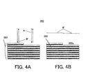
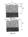
- FIG. 3A parallel light A with an equal phase incident upon a multilayer mirror 300 that uniformly forms a multilayer film 320 on a plane mirror substrate 310 would provide reflected light B having a completely equal phase or reflected wave front B as shown in FIG. 3B.
- wave front B' of the reflected light from part 320a, at which one pair of films form unevenness on the multilayer film 320 forms a phase difference as shown in FIG. 4B.
- FIG. 3 is a schematic typical view showing a relationship between incident light and reflected wave front in a multilayer film having a uniform layer surface.
- FIG. 4 is a schematic typical view showing a relationship between incident light and reflected wave front in a multilayer having a difference of one layer pair according to locations.
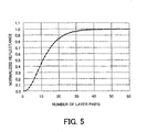
- the reflectance of the multilayer mirror depends upon the number of layer pairs of the multilayer film.
- FIG. 5 is a graph showing reflectance characteristic of the multilayer film, where the abscissa axis shows the periodicity of the multilayer film while the ordinate axis shows the reflectance normalized by the maximum value. Referring to FIG. 5, the reflectance increases with the increased periodicity up to the forty layer pairs, and saturates above the forty layer pairs. If a multilayer film has been layered with sufficient periodicity, e.g., sixty layer pairs after the reflectance saturates, a difference in periodicity in the multilayer film would affect only wave front.
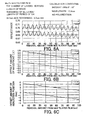
- FIG. 6A is a graph of a relationship between the removal amount of the multilayer film and reflectance
- FIG. 6B shows a graph between the removal amount of the multilayer film and the wave front offset amount, when the EUV light of 13.5 nm is incident at an angle of 10° upon a Mo / Si multilayer mirror.
- a Mo / Si multilayer arranges the Si layer as the uppermost layer to reduce the influence of the oxidization of Mo, and the instant embodiment has calculated on the assumption that the Si layer is located as the uppermost layer. It is understood from FIGs. 6A and 6B that as one layer pair of 6.99 nm is removed from the multilayer film, the wave front of the reflected light moves by about 0.025 wavelength.
- FIG. 6C shows a graph that converts an offset amount of wave front into an offset amount of a spatial reflection position.
- a removal of one layer pair of 6.99 nm from the multilayer film means about 0.2 nm movement of the reflected position in the instant embodiment.
- the coating milling changes the index and wave front in the Mo layer more greatly than those in the Si layer due to a relationship of reflectance.
- the reflectance saturates for the periodicity of a multilayer film that has about sixty layer pairs, a removal of one layer pair would change the wave front without changing the reflectance.
- a multilayer mirror 400 that uniformly forms a multilayer film 420 on a distorted mirror substrate 410.
- the coating milling is an approach to delay a phase, and applied to a point A as an origin having the latest phase.
- the Si layer a little changes the wave front
- the Mo layer changes the wave front greatly and, as described above, is weak to oxidization. Therefore, without special coating, it is not desirable to finish coating milling in the middle of the Mo layer and continuously adjust the wave front.
- the wave front is adjusted discontinuously by removing every layer pair of Mo and Si.
- FIG. 7 is a schematic sectional view of the multilayer mirror 400 that uniformly forms the multilayer film 420 on the distorted mirror surface 410, wherein FIGs. 7A and 7B respectively shows the multilayer mirror 400 before and after the coating milling.
- the wave front aberration caused by the figure error of the mirror substrate 410 may be corrected by removing two layer pairs from the multilayer film 420 at the point B and one layer pair from the multilayer film 420 at the point C.
- FIG. 8A for example, suppose a multilayer mirror 500 that uniformly forms a multilayer film 520 on a mirror substrate 510 that has a point F at a center part above a point E on the edge. Since the point E has relatively the latest phase in the multilayer mirror 500, the coating milling is applied to a point E as an origin.
- the mirror substrate 510 has a figure error of about 0.4 nm between the edge point E and the center point F, and the figure error changes continuously, two layer pairs are removed from the multilayer film 520 at the center point F.
- the wave front aberration caused by the figure error may be corrected by removing one layer pair at both sides.
- FIG. 8 is a schematic sectional view of the multilayer mirror 500 that forms the multilayer film 520 on the mirror substrate 510 that swells at the center point F above the edge point E, wherein FIGs. 8A and 8B respectively shows the multilayer mirror 500 before and after the coating milling.
- the adjustment apparatus 100 includes, as shown in FIG. 2, a measurement pert 110, a removal part 120, and a control part 130.
- the measurement part 110 measures the wave front aberration of the entire optical system, and includes a wave front aberration measurement apparatus, such as a Point Diffraction Interferometer ("PDI").
- a wave front aberration measurement apparatus such as a Point Diffraction Interferometer ("PDI").
- a description will be given of the PDI based on a projection optical system in an exposure apparatus as an example of an optical system.
- a pinhole is located on a surface corresponding to a reticle surface in the exposure apparatus to generate a spherical wave of (EUV, ultraviolet visible, infrared, etc.) light from the pinhole.
- a diffraction grating splits a beam into two located downstream the pinhole, and one beam is introduced into a detector at a wafer surface position through the projection optical system, and the other beam is introduced into a detector as reference wave front.
- the wave front aberration caused by the projection optical system is observed through interference between two wave fronts on the detectors.
- the above method finishes an observation of the wave front aberration at one point on the wafer surface.
- the wave front aberration in the whole projection optical system is measured over the entire illumination area on the reticle by moving a pinhole position on the reticle surface.
- the removal part 120 partially removes the multilayer using, for example, sputtering or ion beam milling.
- the sputtering injects accelerated ions into a surface of the multilayer mirror or a multilayer film strips off atoms, and removes a portion of multilayer film.
- the ion beam milling maintains an ion source in a positive potential state, generates plasma using inert gas, draws inert gas ions from the ion source, and irradiates the ions onto the multilayer mirror.
- the control part 130 is connected to the measurement part 110 and the removal part 120, and the measurement part 110 determines conditions to remove the multilayer film, such as a removal area and removal amount, based on the wave front aberration measured by the measurement part 110, and controls the removal part 120 to remove the part of the multilayer mirror in accordance with the determined condition.
- the control part 130 calculates an adjustment amount of the multilayer mirror, such as a position and an angle, based on the wave front aberration measured by the measurement part 110.
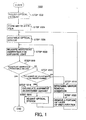
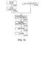
- FIG. 1 is a flowchart for explaining the inventive adjustment method.
- a description will be given of an exemplary adjustment of the projection optical system including a Mo / Si multilayer mirror in an exposure apparatus.
- each Mo / Si multilayer mirror is polished with sufficient surface precision in the projection optical system (step 1002).
- a multilayer film is formed by alternately layering Mo and Si on a mirror surface that has been polished with sufficient surface precision (step 1004).
- the entire mirror layers a multilayer film that a Mo layer has a thickness of about 2 nm and a Si layer has a thickness of about 5 nm.
- the multilayer mirror is assembled into a mirror barrel of the projection optical system (step 1006).
- the measurement part 110 measures the wave front aberration of the projection optical system on the wafer surface (step 1008).
- the wave front aberration is measured using the EUV light having a wavelength to be used.
- the measured wave front aberration is compared with a permissible amount (step 1010), and the assembly into the mirror barrel finishes when the wave front aberration is within the permissible range, e.g., equal to or smaller than 0.4 nm in case of transfer of resolution 30 nm.
- the number of adjustments of a mirror position is compared with the preset number (step 1012), if it is within the preset number, the control part 130 calculates the alignment amount, such as a position and/or angle of the mirror, of the mirror based on the measured wave front aberration result (step 1014).
- the control part 130 may utilize a table that correlates a rotation and movement of each mirror with a change of generated wave front, which table has been obtained through calculation.
- the control part 130 adjusts a mirror in the projection optical system based on a calculated alignment adjustment amount (step 1016).
- the measurement part 110 measures the wave front aberration after a mirror is adjusted by a calculated amount using the EUV light (step 1008).
- the assembly finishes when the measured wave front aberration is within the permissible range (step 1010).
- the procedure is repeated from the measurement of the wave front aberration by the measurement part 110 (step 1008) to the adjustment of mirror (step 1016).
- the alignment follows to minimize the wave front aberration generated in the projection optical system. Since it is difficult that only the adjustment of the mirror position completely eliminates the wave front aberration generated by a surface figure error of the mirror substrate and bending due to the mirror's own weight, the number of adjustments of the mirror position should be preset.
- the wave front aberration measured by the measurement part 110 on the wafer surface is the wave front aberration for the entire projection optical system.
- the coating milling does not have to be provided for each mirror, and a specific mirror is selected as an object of the coating milling to correct the wave front aberration of the entire projection optical system.
- the number of specific mirrors is not limited to one and may be plural.
- the control part 130 determines conditions, such as a correction amount and place, to remove part of the multilayer film in the mirror based on the measurement result of the wave front aberration. After the mirror is taken out of the mirror barrel for coating milling, the removal part 120 removes the multilayer film at a desired position from the mirror (step 1020).
- the mirror is assembled into the mirror barrel after the coating milling (step 1006), and the procedure from the measurement of the wave front aberration by the measurement part 110 (step 1008) to the adjustment of mirror (step 1016) is repeated.
- the wave front aberration does not fall within the permissible range, the mirror is corrected by the coating milling and similar steps are repeated.
- light such as ultraviolet light, visual light, and infrared light
- light such as ultraviolet light, visual light, and infrared light
- the wave front aberration measurement apparatus that has been incorporated into an exposure apparatus itself, which will be described later, may measure the wave front aberration using light different from the exposure light, while the projection optical system is incorporated into the exposure apparatus.
- the multilayer film in the area that has experienced coating milling includes such steps that wave front observed using the ultraviolet light, visible light, and infrared light greatly shifts unlike the observation of the wave front aberration of the EUV wavelength. Therefore, in measuring the wave front aberration using the ultraviolet light, visible light, and infrared light, it is difficult that the procedure is repeated from the step 1006 to the step 1020 for plural times of coating milling as discussed above.
- Step 1016 measures the wave front aberration at the exposure wavelength.
- the above coating milling is provided.
- the above wave front aberration measurement apparatus uses light other than the exposure light and measures a wave front of an optical system so as to obtain mirror information, such as an angle and position of the mirror (step 1017).
- the mirror is taken out of the mirror barrel and the coating milling is provided. After the milling ends, the mirror is again incorporated into the mirror barrel and the information is used to reproduce the mirror's position, etc.
- the light other than the exposure light includes, for example, ultraviolet light, visible light, and infrared light.
- the measurement part 110 measures the wave front aberration, and the control part 130 determines conditions to remove part of multilayer film in the mirror based on the measurement result (step 1018).
- the mirror as an object of the coating milling is taken out of the mirror barrel, and the removal part 120 removes multilayer film at desired location (step 1020).
- the mirror is assembled into an optical system (step 1022) and the wave front aberration is measured (step 1024).
- the wave front measured after the coating milling is observed to show that the wave front shifts greatly from that measured in the step 1017.
- a method of removing the area that has experienced the coating milling may provide a mask on the multilayer mirror to shield light corresponding to the area that has experienced the coating milling, or delete from wave front measurement data in data processing, data corresponding to the area that has experienced the coating milling.
- the measured wave front aberration is compared with a permissible amount (step 1026), and the adjustment to the optical system is completed when the wave front aberration is within the permissible range.
- the number of adjustments of a mirror position is compared with the preset number (step 1028). If it is within the preset number, the alignment adjustment is repeated from the step 1022 to the step 1032.
- the permissible value is determined by the mirror information obtained at the step 1017.
- step 1028 the procedure from polishing of the optical element (step 1002) is repeated again.
- This adjustment method may provide a projection optical system whose wave front aberration has been corrected.
- the step 1008 uses the exposure light or the EUV light to measure the wave front aberration.
- the wave front measurement using the exposure wavelength often needs large facility, such as a synchrotron light source.
- the wave front measurement using the light other than the exposure light provides information on the wave front measured by the exposure light, without requiring the large facility.
- the relationship between the wave front measured by the exposure light and the wave front measured by the light other than the exposure light may be obtained from simulation, etc.
- an optical system having ideal imaging performance for the EUV light and then the wave front aberration on an imaging surface is calculated by simulation when the light other than the exposure light (e.g. ultraviolet light, visible light, and infrared light) is used.
- the wave front aberration that has been converted into that for the EUV light reduces by minimizing a square sum of a difference between the wave front aberration measured with the light other than the exposure light and the aberration obtained from the above simulation.
- a conversion equation from the wave front aberration measured with the light other than the exposure light to the wave front aberration measured with the exposure light may be experimentally determined.
- a base mirror barrel is prepared, the wave front aberration is measured with the EUV light, and the wave front aberration is reduced down to accuracy enough for exposure. Then, the wave front aberration of the base mirror barrel is measured, for example, with the visible light. The wave front aberration on imaging surfaces for each of the EUV light and visible light is developed into Zernike's polynomial, and a difference is calculated.
- the wave front aberration is measured by the visible light, and developed into Zernike's polynomial.
- the wave front aberration for the EUV light may be calculated by adding known difference.
- the information on the wave front for the exposure light may be obtained from the wave front measurement.
- the light such as ultraviolet light, visible light and infrared light, other than the exposure light.
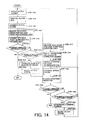
- FIG. 14 shows a flow of the optical system adjustment in the third embodiment.
- the procedure to assemble an optical system up to the step 1006 is the same as those in the adjustment flows in the first embodiment and modification.
- the wave front measurement in the step 1008 uses the light other than the exposure light.
- the measured wave front is converted in the step 1009 into the wave front measured with the exposure light by the above method.
- the adjustment follows so that the amount of the converted wave front aberration may be below the permissible value.
- the following adjustment flow is the same as that of the first embodiment shown in FIG. 12, but the wave front measurement step 1017 using the light other than the exposure light in FIG. 14 may be omitted since the step 1017 is replaceable with the wave front measurement step 1008 in FIG. 14.
- the wave front aberration for the EUV light may be obtained from the wave front measurement using the light other than the exposure light (e.g. ultraviolet light, visible light, and infrared light), given a relationship of the wave front aberration between the light other than the exposure light and the EUV light. Therefore, the large facility, such as a synchrotron light source, is not necessary for manufacture, and an exposure apparatus with simple structure but having high imaging performance may be provided.
- the light other than the exposure light e.g. ultraviolet light, visible light, and infrared light
- the first to third embodiments use the adjustment. apparatus 100 to measure wave front aberration (in steps 1008 and 1024) for optical system assembly (in steps 1006 and 1022).
- This requires an additional step of assembling a projection optical system into an exposure apparatus after the adjustment apparatus finally adjusts the projection optical system, and the projection optical system is likely to generate aberration upon this assembly. Therefore, the above PDI is mounted onto the exposure apparatus so as to assemble the optical system and measure the wave front aberration.
- a description will now be given of a concrete method of measuring the wave front aberration applicable to this case using an exposure apparatus 700, which will be described in detail later with reference to FIG. 9.
- a mirror is incorporated into a projection optical system 730 of the exposure apparatus (steps 1006 and 1022). Then, a wafer stage 745 and a mask stage 725 are driven so as to arrange, in an exposure area, a PS / PDI mask 778 on the wafer stage and a pinhole 776 on the mask stage.
- a light source 770 is.provided which emits light (such as ultraviolet light, visual light, and infrared light) having a wavelength different from that of the exposure light, and the light from the light source 770 is introduced to the pinhole 776 provided on the mask stage 725 via the optical fiber 772 so as to generate spherical wave.
- the spherical wave is then divided into two by a diffraction grating 774 mounted onto a grating stage (not shown), and the wave front aberration of the projection optical system 730 may be measured on the exposure apparatus (steps 1008 and 1024) by detecting respective divided beams using detector means 780 (such as a CCD) via the projection optical system 730 and the PS / PDI mask shown in FIG.
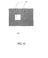
- FIG. 13 is a view of the PS / PDI mask 780 provided on the wafer stage 745, which has openings 781.
- the wave front aberration measurement apparatus installed on the exposure apparatus may be used for the subsequent optical system assembly and wave front aberration measurement, even when the EUV light is used to measure the wave front aberration for coating milling.
- a pinhole plate is arranged on the mask stage instead of a mask 720.
- FIG. 9 is a schematic structure of an illustrative inventive exposure apparatus 700.
- the inventive exposure apparatus 700 is a projection exposure apparatus 700 that uses EUV light with a wavelength of 13.4 nm as exposure light for step-and-scan exposure.
- the exposure apparatus 700 includes an illumination apparatus 710, a mask 720, a mask stage 725 that mounts the mask 720, a projection optical system 730, an object to be exposed 740, a wafer stage 745 that mounts the object 740, and an alignment detecting mechanism 750, and a focus position detecting mechanism 760.
- An optical path through which EUV light passes is preferably maintained in a vacuum atmosphere "A" due to low transmittance to air of the EUV light, as shown in FIG. 9.
- the illumination apparatus 710 uses arc-shaped EUV light, for example, with a wavelength of 13.4 corresponding to an arc-shaped field of the projection optical system 730 to illuminate the mask 720, and includes an EUV light source 712 and illumination optical system 714.
- the EUV light source 712 employs, for example, a laser plasma light source. It generates high temperature plasma by irradiating a pulsed laser beam with high intensity onto a target material in a vacuum chamber, and uses the EUV light, for example, with a wavelength of about 13.4 nm, which has been emitted from the plasma.
- the target material may use a metallic thin film, an inert gas, a liquid-drop, etc., and the target supply unit may use a gas jet and so on.
- the pulse laser is usually driven with a higher repetitive frequency, such as several kHz, for increased average intensity of radiated EUV light.
- the illumination optical system 714 includes a condenser mirror, an optical integrator, etc.
- the condenser mirror serves to collect the EUV light that is isotropically irradiated from the laser plasma.
- the optical integrator serves to uniformly illuminate the mask 720 with a predetermined NA. An aperture to limit the illumination area to an arc shape is also provided.
- the mask 720 is a reflection-type mask that forms a circuit pattern or image to be transferred, and supported and driven by the mask stage 725.
- the diffracted light from the mask 720 is reflected by the projection optical system 730 and projected onto the object 740.
- the exposure apparatus 700 is a step-and-scan exposure apparatus, and projects a reduced size of the pattern on the mask 720 on the object 740 by scanning the mask 720 and the object 740.
- the mask stage 725 supports the mask 720 and is connected to a moving mechanism (not shown).
- the mask stage 725 may use any structure known in the art.
- a moving mechanism (not shown) may include a linear motor etc., and drives the mask stage 725 at least in a direction X and moves the mask 720.
- the exposure apparatus 700 assigns the direction X to scan the mask 720 or the object 740, a direction Y perpendicular to the direction X, and a direction Z perpendicular to the mask 720 or the object 740.
- the projection optical system 730 uses plural multilayer mirrors to project a reduced size of a pattern formed on the mask 720 onto the object.
- the number of mirrors is about four to six.
- the mask 720 and object 740 are simultaneously scanned to transfer a wide area that is an arc-shaped area or ring field apart from the optical axis by a predetermined distance.
- the projection optical system 730 has a NA of about 0.1 to 0.3.
- the inventive adjustment apparatus 100 and adjustment method 1000 are applicable to an adjustment of the multilayer mirror in the projection optical system 730 for reduced wave front aberration and improved imaging performance.
- a photoresist application step includes a pretreatment, an adhesion accelerator application treatment, a photoresist application treatment, and a pre-bake treatment.
- the pretreatment includes cleaning, drying, etc.
- the adhesion accelerator application treatment is a surface reforming process so as to enhance the adhesion between the photoresist and a base (i.e., a process to increase the hydrophobicity by applying a surface active agent), through a coat or vaporous process using an organic film such as HMDS (Hexamethyl-disilazane).
- the pre-bake treatment is a baking (or burning) step, softer than that after development, which removes the solvent.
- An object to be exposed 740 is held onto the wafer stage 745 by a wafer chuck.
- the wafer stage 745 moves the object 740, for example, using a linear stage in XYZ directions.
- the mask 720 and the object are synchronously scanned-
- the positions of the mask stage 725 and wafer stage 745 are monitored, for example, by a laser interferometer, and driven at a constant speed ratio.
- the alignment detection mechanism 750 measures a positional relationship between the position of the mask 720 and the optical axis of the projection optical system 730, and a positional relationship between the position of the object 740 and the optical axis of the projection optical system 730, and sets positions and angles of the mask stage 725 and the wafer stage 745 so that a projected image of the mask 720 may be positioned in place on the object 740.
- a focus detection optical system 760 measures a focus position in the direction Z on the object 740 surface, and control over a position and angle of the wafer stage 745 may always maintain the object 740 surface at an imaging position of the projection optical system 730 during exposure.
- the EUV light emitted from the illumination apparatus 710 illuminates the mask 720, and images a pattern formed on the mask 720 onto the object 740 surface.
- the instant embodiment uses an arc or ring shaped image plane, scans the mask 720 and object 740 at a speed ratio corresponding to a reduction ratio to expose the entire surface of the mask 720.
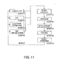
- FIG. 10 is a flowchart for explaining a fabrication of devices (i.e., semiconductor chips such as IC and LSI, LCDs, CCDs, etc.).
- a fabrication of a semiconductor chip as an example.
- Step 1 circuit design
- Step 2 mask fabrication
- Step 3 wafer preparation
- Step 4 wafer process
- a pretreatment forms actual circuitry on the wafer through photolithography using the mask and wafer.
- Step 5 (assembly), which is also referred to as a posttreatment, forms into a semiconductor chip the wafer formed in Step 4 and includes an assembly step (e.g., dicing, bonding), a packaging step (chip sealing), and the like.
- Step 6 (inspection) performs various tests for the semiconductor device made in Step 5, such as a validity test and a durability test. Through these steps, a semiconductor device is finished and shipped (Step 7).
- FIG. 11 is a detailed flowchart of the wafer process in Step 4 in FIG. 10.
- Step 11 oxidation
- Step 12 CVD
- Step 13 electrode formation
- Step 14 ion implantation
- Step 15 resist process
- Step 16 exposure
- Step 17 development
- Step 18 etching
- Step 19 resist stripping
- the present invention is not limited to these preferred embodiments, and various variations and modifications may be made without departing from the scope of the present invention.
- the present invention is applicable to an optical system that uses a multilayer mirror and other optical elements, such as a lens and diffraction grating.
- the present invention is also applicable, for example, to a projection optical system for ultraviolet light with a wavelength of 200 nm or smaller such as ArF excimer laser and F 2 laser, as well as an exposure apparatus that exposes a large screen through scanning / non-scanning.
- the inventive adjustment apparatus and method may provide an optical system that stably transfer a fine pattern using the EUV light as well as other types of light by removing part of the multilayer mirror based on the wave front aberration generated in the entire optical system that has a multilayer mirror, and reducing the wave front aberration. Therefore, an exposure apparatus that uses such an optical system may provide high-quality devices with good exposure performance.
Landscapes
- Physics & Mathematics (AREA)
- General Physics & Mathematics (AREA)
- Engineering & Computer Science (AREA)
- Chemical & Material Sciences (AREA)
- Optics & Photonics (AREA)
- Spectroscopy & Molecular Physics (AREA)
- General Engineering & Computer Science (AREA)
- High Energy & Nuclear Physics (AREA)
- Nanotechnology (AREA)
- Theoretical Computer Science (AREA)
- Crystallography & Structural Chemistry (AREA)
- Mathematical Physics (AREA)
- Exposure And Positioning Against Photoresist Photosensitive Materials (AREA)
- Exposure Of Semiconductors, Excluding Electron Or Ion Beam Exposure (AREA)
- Testing Of Optical Devices Or Fibers (AREA)
- Mounting And Adjusting Of Optical Elements (AREA)
Applications Claiming Priority (2)
| Application Number | Priority Date | Filing Date | Title |
|---|---|---|---|
| JP2002220389 | 2002-07-29 | ||
| JP2002220389 | 2002-07-29 |
Publications (2)
| Publication Number | Publication Date |
|---|---|
| EP1387220A2 true EP1387220A2 (de) | 2004-02-04 |
| EP1387220A3 EP1387220A3 (de) | 2007-01-03 |
Family
ID=30112911
Family Applications (1)
| Application Number | Title | Priority Date | Filing Date |
|---|---|---|---|
| EP03254724A Withdrawn EP1387220A3 (de) | 2002-07-29 | 2003-07-28 | Justiermethode und -apparat eines optischen Systems, sowie Belichtungsapparat |
Country Status (4)
| Country | Link |
|---|---|
| US (1) | US7083290B2 (de) |
| EP (1) | EP1387220A3 (de) |
| KR (1) | KR100541487B1 (de) |
| TW (1) | TWI239033B (de) |
Cited By (6)
| Publication number | Priority date | Publication date | Assignee | Title |
|---|---|---|---|---|
| WO2005031466A1 (en) * | 2003-09-26 | 2005-04-07 | Carl Zeiss Smt Ag | Method of determining optical properties and projection exposure system comprising a wave front detection system |
| DE10345783A1 (de) * | 2003-10-01 | 2005-04-21 | Zeiss Carl Sms Gmbh | Optisches Abbildungssystem |
| EP1568976A1 (de) * | 2004-02-27 | 2005-08-31 | Canon Kabushiki Kaisha | Belichtungsapparat ausgestattet mit Messvorrichtung |
| EP1594007A2 (de) | 2004-05-07 | 2005-11-09 | Canon Kabushiki Kaisha | Zusammenstellungs- und Einstellungsverfahren für ein optisches System und dieses enthaltender Belichtungsapparat |
| WO2007121990A1 (de) | 2006-04-24 | 2007-11-01 | Carl Zeiss Smt Ag | Projektionsbelichtungssystem und verwendung desselben |
| EP1717639A3 (de) * | 2005-04-25 | 2009-07-08 | Canon Kabushiki Kaisha | Belichtungsgerät |
Families Citing this family (18)
| Publication number | Priority date | Publication date | Assignee | Title |
|---|---|---|---|---|
| US7843632B2 (en) * | 2006-08-16 | 2010-11-30 | Cymer, Inc. | EUV optics |
| JP2005321564A (ja) * | 2004-05-07 | 2005-11-17 | Canon Inc | 多層膜が形成された光学素子の製造方法 |
| KR101316633B1 (ko) | 2004-07-28 | 2013-10-15 | 삼성디스플레이 주식회사 | 다결정 규소용 마스크 및 이의 제조방법과, 이를 이용한박막트랜지스터의 제조방법 |
| JP2007041529A (ja) * | 2005-06-30 | 2007-02-15 | Konica Minolta Opto Inc | 投射光学系の製造方法及び投射光学系 |
| KR100809329B1 (ko) * | 2006-09-08 | 2008-03-07 | 삼성전자주식회사 | 광학계의 수차를 보정하기 위한 미러를 포함하는포토리소그래피 장치 및 수차 보정부를 포함하는 미러 |
| EP2157584A3 (de) * | 2008-08-14 | 2011-07-13 | ASML Netherlands B.V. | Strahlungsquelle, Lithografiegerät und Herstellungsverfahren für ein Bauteil |
| WO2011120009A1 (en) * | 2010-03-26 | 2011-09-29 | Lawrence Livermore National Security, Llc | Multi-pass amplifier architecture for high power laser systems |
| DE102010038697B4 (de) * | 2010-07-30 | 2012-07-19 | Carl Zeiss Smt Gmbh | Verfahren und Vorrichtung zur Qualifizierung einer Optik einer Projektionsbelichtungsanlage für die Mikrolithographie |
| WO2012102313A1 (ja) * | 2011-01-26 | 2012-08-02 | 旭硝子株式会社 | フォトマスクの製造方法 |
| DE102011084117A1 (de) | 2011-10-07 | 2013-04-11 | Carl Zeiss Smt Gmbh | Reflektives optisches Element für den EUV-Wellenlängenbereich, Verfahren zur Erzeugung und zur Korrektur eines solchen Elements, Projektionsobjektiv für die Mikrolithographie mit einem solchen Element und Projektionsbelichtungsanlage für die Mikrolithographie mit einem solchen Projektionsobjektiv |
| DE102013202372A1 (de) * | 2013-02-14 | 2013-12-19 | Carl Zeiss Smt Gmbh | Verfahren zur Herstellung einer elektromagnetische Wellen beugenden Struktur für eine Wellenfrontquelle |
| WO2019121491A1 (en) * | 2017-12-22 | 2019-06-27 | Asml Netherlands B.V. | Patterning process improvement involving optical aberration |
| DE102018211596A1 (de) | 2018-07-12 | 2020-01-16 | Carl Zeiss Smt Gmbh | Verfahren zur Herstellung eines reflektierenden optischen Elementes einer Projektionsbelichtungsanlage und reflektierendes optisches Element für eine Projektionsbelichtungsanlage, Projektionsobjektiv und Projektionsbelichtungsanlage |
| DE102020203753A1 (de) | 2020-03-24 | 2021-09-30 | Carl Zeiss Smt Gmbh | Projektionsbelichtungsanlage für die Halbleiterlithographie |
| DE102020203750A1 (de) | 2020-03-24 | 2021-09-30 | Carl Zeiss Smt Gmbh | Vorrichtung zur Erfassung einer Temperatur, Anlage zur Herstellung eines optischen Elementes und Verfahren zur Herstellung eines optischen Elementes |
| DE102022200976A1 (de) | 2022-01-31 | 2023-01-05 | Carl Zeiss Smt Gmbh | Kalibrierkörper und Verfahren zur Kalibrierung |
| DE102022210037A1 (de) | 2022-09-23 | 2024-03-28 | Carl Zeiss Smt Gmbh | Anordnung zum Tempern mindestens eines Teilbereichs eines optischen Elementes |
| DE102023208563A1 (de) | 2023-09-06 | 2025-03-06 | Carl Zeiss Smt Gmbh | Bearbeitung eines optischen Elements für eine Projektionsbelichtungsanlage |
Family Cites Families (9)
| Publication number | Priority date | Publication date | Assignee | Title |
|---|---|---|---|---|
| US171922A (en) * | 1876-01-11 | Improvement in glue-pots | ||
| JP3706691B2 (ja) | 1996-08-26 | 2005-10-12 | キヤノン株式会社 | X線縮小投影露光装置及びこれを用いた半導体デバイス製造方法 |
| JP2000091209A (ja) * | 1998-09-14 | 2000-03-31 | Nikon Corp | 露光装置の製造方法、露光装置、及びデバイス製造方法 |
| AU2807401A (en) * | 1999-11-29 | 2001-06-12 | Tohoku Techno Arch Co., Ltd. | Optical element such as multilayer film reflection mirror, production method therefor and device using it |
| US20020171922A1 (en) * | 2000-10-20 | 2002-11-21 | Nikon Corporation | Multilayer reflective mirrors for EUV, wavefront-aberration-correction methods for same, and EUV optical systems comprising same |
| JP2002131489A (ja) | 2000-10-20 | 2002-05-09 | Nikon Corp | 多層膜反射鏡およびeuv露光装置 |
| EP1291680A2 (de) * | 2001-08-27 | 2003-03-12 | Nikon Corporation | Multischicht-Spiegel für das ferne UV, und Hertellungsverfahren für solche Spiegel mit verringerten Aberration |
| JP2003077805A (ja) | 2001-09-03 | 2003-03-14 | Nikon Corp | 光学系の製造方法およびeuv露光装置 |
| JP4266673B2 (ja) * | 2003-03-05 | 2009-05-20 | キヤノン株式会社 | 収差測定装置 |
-
2003
- 2003-07-28 EP EP03254724A patent/EP1387220A3/de not_active Withdrawn
- 2003-07-29 US US10/629,879 patent/US7083290B2/en not_active Expired - Fee Related
- 2003-07-29 TW TW092120707A patent/TWI239033B/zh not_active IP Right Cessation
- 2003-07-29 KR KR1020030052218A patent/KR100541487B1/ko not_active Expired - Fee Related
Cited By (12)
| Publication number | Priority date | Publication date | Assignee | Title |
|---|---|---|---|---|
| WO2005031466A1 (en) * | 2003-09-26 | 2005-04-07 | Carl Zeiss Smt Ag | Method of determining optical properties and projection exposure system comprising a wave front detection system |
| US7230220B2 (en) | 2003-09-26 | 2007-06-12 | Carl Zeiss Smt Ag | Method of determining optical properties and projection exposure system comprising a wavefront detection system |
| DE10345783A1 (de) * | 2003-10-01 | 2005-04-21 | Zeiss Carl Sms Gmbh | Optisches Abbildungssystem |
| EP1568976A1 (de) * | 2004-02-27 | 2005-08-31 | Canon Kabushiki Kaisha | Belichtungsapparat ausgestattet mit Messvorrichtung |
| US7619748B2 (en) | 2004-02-27 | 2009-11-17 | Canon Kabushiki Kaisha | Exposure apparatus mounted with measuring apparatus |
| EP1594007A2 (de) | 2004-05-07 | 2005-11-09 | Canon Kabushiki Kaisha | Zusammenstellungs- und Einstellungsverfahren für ein optisches System und dieses enthaltender Belichtungsapparat |
| EP1594007A3 (de) * | 2004-05-07 | 2007-01-10 | Canon Kabushiki Kaisha | Zusammenstellungs- und Einstellungsverfahren für ein optisches System und dieses enthaltender Belichtungsapparat |
| US7280184B2 (en) | 2004-05-07 | 2007-10-09 | Canon Kabushiki Kaisha | Assembly and adjusting method of optical system, exposure apparatus having the optical system |
| EP1717639A3 (de) * | 2005-04-25 | 2009-07-08 | Canon Kabushiki Kaisha | Belichtungsgerät |
| US7602473B2 (en) | 2005-04-25 | 2009-10-13 | Canon Kabushiki Kaisha | Exposure apparatus and device manufacturing method using the same |
| WO2007121990A1 (de) | 2006-04-24 | 2007-11-01 | Carl Zeiss Smt Ag | Projektionsbelichtungssystem und verwendung desselben |
| US8908149B2 (en) | 2006-04-24 | 2014-12-09 | Carl Zeiss Smt Gmbh | Projection exposure system and use thereof |
Also Published As
| Publication number | Publication date |
|---|---|
| TW200405403A (en) | 2004-04-01 |
| KR20040011380A (ko) | 2004-02-05 |
| US7083290B2 (en) | 2006-08-01 |
| EP1387220A3 (de) | 2007-01-03 |
| US20040095662A1 (en) | 2004-05-20 |
| TWI239033B (en) | 2005-09-01 |
| KR100541487B1 (ko) | 2006-01-11 |
Similar Documents
| Publication | Publication Date | Title |
|---|---|---|
| US7083290B2 (en) | Adjustment method and apparatus of optical system, and exposure apparatus | |
| US7771898B2 (en) | Multilayer mirror, evaluation method, exposure apparatus, device manufacturing method | |
| KR100554256B1 (ko) | 광학 결상 시스템 작동방법, 리소그래피 투영장치,디바이스 제조방법, 및 그것에 의해 제조된 디바이스 | |
| US7952726B2 (en) | Measurement apparatus, exposure apparatus having the same, and device manufacturing method | |
| EP2198344B1 (de) | Mikrolithographische projektionsbelichtungsvorrichtung | |
| US8945802B2 (en) | Flare-measuring mask, flare-measuring method, and exposure method | |
| US20040174533A1 (en) | Wavefront aberration measuring apparatus | |
| US7348582B2 (en) | Light source apparatus and exposure apparatus having the same | |
| JP3981664B2 (ja) | 検査方法およびデバイス製造方法 | |
| US7692799B2 (en) | Measurement apparatus, exposure apparatus, and device fabrication method | |
| US20090147364A1 (en) | Exposure mirror and exposure apparatus having same | |
| US7142284B2 (en) | Position detector, position detecting method, and exposure apparatus having the same | |
| US20050134980A1 (en) | Projection objective and method for its manufacture | |
| US20040227920A1 (en) | Illumination apparatus, projection exposure apparatus, and device fabrication method | |
| US20060092397A1 (en) | Lithographic apparatus and device manufacturing method | |
| US7543948B2 (en) | Multilayer mirror manufacturing method, optical system manufacturing method, exposure apparatus, and device manufacturing method | |
| KR20010015698A (ko) | 투영노광방법 및 장치 | |
| US7295326B2 (en) | Apparatus and method for measuring the optical performance of an optical element | |
| KR20010006578A (ko) | 광학 보정 플레이트, 및 전사 투영 장치에의 적용 | |
| JP3958261B2 (ja) | 光学系の調整方法 | |
| EP1569036B1 (de) | Belichtungsapparat und Verfahren zur Herstellung einer Vorrichtung | |
| US7102734B2 (en) | Exposure apparatus | |
| JP2004134444A (ja) | 極短紫外線光学系の光学特性測定方法及び装置、並びに極短紫外線光学系の製造方法 | |
| WO2005055295A1 (ja) | 露光方法及び装置、並びにデバイス製造方法 |
Legal Events
| Date | Code | Title | Description |
|---|---|---|---|
| PUAI | Public reference made under article 153(3) epc to a published international application that has entered the european phase |
Free format text: ORIGINAL CODE: 0009012 |
|
| AK | Designated contracting states |
Kind code of ref document: A2 Designated state(s): AT BE BG CH CY CZ DE DK EE ES FI FR GB GR HU IE IT LI LU MC NL PT RO SE SI SK TR |
|
| AX | Request for extension of the european patent |
Extension state: AL LT LV MK |
|
| PUAL | Search report despatched |
Free format text: ORIGINAL CODE: 0009013 |
|
| AK | Designated contracting states |
Kind code of ref document: A3 Designated state(s): AT BE BG CH CY CZ DE DK EE ES FI FR GB GR HU IE IT LI LU MC NL PT RO SE SI SK TR |
|
| AX | Request for extension of the european patent |
Extension state: AL LT LV MK |
|
| 17P | Request for examination filed |
Effective date: 20070703 |
|
| AKX | Designation fees paid |
Designated state(s): DE FR GB IT NL |
|
| 17Q | First examination report despatched |
Effective date: 20071213 |
|
| STAA | Information on the status of an ep patent application or granted ep patent |
Free format text: STATUS: THE APPLICATION HAS BEEN WITHDRAWN |
|
| 18W | Application withdrawn |
Effective date: 20111005 |